

DipTrace complete help
- 1. Package Overview
- 2. Schematic
- 2.1. User interface
- 2.1.1. Main window
- 2.1.2. Toolbars
- 2.1.3. Place Component panel
- 2.1.4. Design Manager
- 2.1.5. Status Bar
- 2.1.6. Main menu
- 2.1.7. Object submenus
- 2.1.8. Modes of operation
- 2.1.9. Hotkeys
- 2.1.10. Environment Variables
- 2.2. Working with files
- 2.2.1. Create project
- 2.2.2. Open project
- 2.2.3. Save project
- 2.2.4. Schematic to PCB
- 2.2.5. Back Annotate
- 2.2.6. Import
- 2.2.7. Export
- 2.2.8. Schematic information
- 2.3. Working with libraries
- 2.4. View functions
- 2.5. Objects
- 2.5.1. Component
- 2.5.2. Net
- 2.5.3. Differential pair
- 2.5.4. Bus
- 2.5.5. Shape
- 2.5.6. Text
- 2.5.7. Table
- 2.5.8. Bus connector
- 2.5.9. Hierarchy
- 2.5.10. Search objects
- 2.6. Edit functions
- 2.7. Verification
- 2.8. Plugins
- 2.9. Print, Sheet Setup
- 2.1. User interface
- 3. PCB Layout
- 3.1. User interface
- 3.1.1. Main window
- 3.1.2. Toolbars
- 3.1.3. Place Component panel
- 3.1.4. Design Manager
- 3.1.5. Status Bar
- 3.1.6. Main menu
- 3.1.7. Object submenus
- 3.1.8. Modes of operation
- 3.1.9. Hotkeys
- 3.1.10. Environment Variables
- 3.2. Working with files
- 3.2.1. Create a circuit board
- 3.2.2. Open PCB
- 3.2.3. Save PCB
- 3.2.4. Update Layout from schematic
- 3.2.5. Update Layout from Netlist
- 3.2.6. Import
- 3.2.6.1. DipTrace ASCII
- 3.2.6.2. DXF
- 3.2.6.3. Gerber
- 3.2.6.4. N/C Drill (Excellon)
- 3.2.6.5. ODB++
- 3.2.6.6. Altium ASCII
- 3.2.6.7. Eagle PCB
- 3.2.6.8. EasyEDA Pro
- 3.2.6.9. KiCAD
- 3.2.6.10. OrCAD Min Interchange
- 3.2.6.11. P-CAD ASCII
- 3.2.6.12. P-CAD PDIF
- 3.2.6.13. PADS ASCII 2005
- 3.2.6.14. Pulsonix
- 3.2.6.15. Sprint-Layout 6.0 Text IO
- 3.2.6.16. Autorouter SES
- 3.2.6.17. Netlist
- 3.2.6.18. 3DS, STEP, VRML, IGES
- 3.2.7. Export
- 3.2.7.1. DipTrace ASCII
- 3.2.7.2. DXF
- 3.2.7.3. Gerber RS-274X
- 3.2.7.4. Gerber X2
- 3.2.7.5. N/C Drill (Excellon)
- 3.2.7.6. ODB++
- 3.2.7.7. IPC-2581
- 3.2.7.8. IPC-D-356A
- 3.2.7.9. Mach 2/3 Drill
- 3.2.7.10. OrCAD TAP Drill
- 3.2.7.11. Bill of Materials
- 3.2.7.12. Pick and Place
- 3.2.7.13. Solder Paste Dispensing
- 3.2.7.14. P-CAD ASCII
- 3.2.7.15. PADS ASCII 2005
- 3.2.7.16. OrCAD Min Interchange
- 3.2.7.17. Autorouter DSN
- 3.2.7.18. 3D PCB model
- 3.2.7.19. Eagle XML
- 3.2.7.20. Order PCB
- 3.2.8. Layout information
- 3.2.9. Panelizing
- 3.3. Working with libraries
- 3.4. View functions
- 3.4.1. Toolbars
- 3.4.2. Scaling/Panning
- 3.4.3. Layers/Objects/Properties
- 3.4.4. Ratlines
- 3.4.5. Net highlight and color
- 3.4.6. Component markings
- 3.4.7. Pad/ Trace Markings
- 3.4.8. Assembly Layer
- 3.4.9. Jumper wires
- 3.4.10. Pad numbers
- 3.4.11. Grid
- 3.4.12. Origin
- 3.4.13. Titles
- 3.4.14. Mirror design
- 3.4.15. Measurement units
- 3.4.16. Line width
- 3.4.17. Graphics mode
- 3.4.18. Precision
- 3.4.19. Colors
- 3.5. Objects
- 3.5.1. Component
- 3.5.2. Net
- 3.5.3. Via
- 3.5.4. Differential pair
- 3.5.4.1. Review
- 3.5.4.2. Create differential pair
- 3.5.4.3. Route differential pair
- 3.5.4.4. Neck differential pair
- 3.5.4.5. Edit differential pair
- 3.5.4.6. Phase tuning
- 3.5.4.7. Signal delay
- 3.5.4.8. Remove differential pair
- 3.5.4.9. Define paired pads
- 3.5.4.10. Diff pair properties
- 3.5.4.11. Differential Pair Manager
- 3.5.5. Shape
- 3.5.6. Text
- 3.5.7. Picture
- 3.5.8. Table
- 3.5.9. Copper pour
- 3.5.10. Board
- 3.5.11. Board cutout
- 3.5.12. Group
- 3.5.13. Pad (single)
- 3.5.14. Mounting hole
- 3.5.15. Fiducial
- 3.5.16. Planar Inductor
- 3.5.17. Dimensions
- 3.5.18. Search layout objects
- 3.6. Editing objects
- 3.7. Placement
- 3.8. Routing
- 3.8.1. Routing steps
- 3.8.2. Adding ratlines
- 3.8.3. Connection Manager
- 3.8.4. Routing setup
- 3.8.5. Interactive Routing Setup
- 3.8.6. Trace templates
- 3.8.7. Routing traces
- 3.8.8. Editing traces
- 3.8.9. Routing differential pairs
- 3.8.10. Editing differential pairs
- 3.8.11. Editing objects
- 3.8.12. Measuring trace length
- 3.8.13. Length matching
- 3.8.14. Fanout
- 3.8.15. Autorouting
- 3.8.15.1. Grid Router
- 3.8.15.2. Shape Router
- 3.8.16. Electra/Specctra integration
- 3.8.17. Hierarchy blocks
- 3.9. PCB Calculators
- 3.10. Verification
- 3.11. Working with layers
- 3.12. Printing, Sheet Setup
- 3.13. 3D preview & export
- 3.14. Plugins
- 3.1. User interface
- 4. Component Editor
- 4.1. User interface
- 4.1.1. Main window
- 4.1.2. Toolbars
- 4.1.3. Status Bar
- 4.1.4. Library Manager panel
- 4.1.5. Main menu
- 4.1.6. Object submenus
- 4.1.7. Modes of operation
- 4.1.8. Hotkeys
- 4.1.9. Environment Variables
- 4.2. Working with libraries
- 4.2.1. General properties
- 4.2.2. Library groups
- 4.2.3. Library setup
- 4.2.4. Create
- 4.2.5. Open
- 4.2.6. Save
- 4.2.7. Bulk Update of Patterns
- 4.2.8. Templates
- 4.2.9. Search components
- 4.2.10. Search at SnapEDA
- 4.2.11. Working with components
- 4.2.12. Verification
- 4.2.13. Import/Export
- 4.2.13.1. DipTrace ASCII import
- 4.2.13.2. DipTrace XML import
- 4.2.13.3. Eagle import
- 4.2.13.4. EasyEDA Pro
- 4.2.13.5. P-CAD import
- 4.2.13.6. Altium ASCII
- 4.2.13.7. PADS import
- 4.2.13.8. KiCAD import
- 4.2.13.9. DipTrace ASCII export
- 4.2.13.10. DipTrace XML export
- 4.2.13.11. Eagle XML export
- 4.2.13.12. BSDL pinlist
- 4.2.13.13. Pinlists
- 4.3. Designing components
- 4.3.1. Review, properties
- 4.3.2. Additional fields
- 4.3.3. Pins
- 4.3.4. Shapes
- 4.3.5. Text
- 4.3.6. Multi-part component
- 4.3.7. Aligning objects
- 4.3.8. Edit component
- 4.3.9. Changing the symbol style
- 4.3.10. Pad signal delay
- 4.3.11. Making buses, pin positioning
- 4.3.12. Attached pattern
- 4.3.13. SPICE Model
- 4.3.14. Pin Manager
- 4.3.15. Insert from library
- 4.4. View functions
- 4.5. Edit functions
- 4.1. User interface
- 5. Pattern Editor
- 5.1. User interface
- 5.1.1. Main window
- 5.1.2. Toolbars
- 5.1.3. Library Manager panel
- 5.1.4. Status Bar
- 5.1.5. Main menu
- 5.1.6. Objects submenus
- 5.1.7. Modes of operation
- 5.1.8. Hotkeys
- 5.1.9. Environment Variables
- 5.2. Working with libraries
- 5.2.1. General properties
- 5.2.2. Library groups
- 5.2.3. Library setup
- 5.2.4. Create
- 5.2.5. Open
- 5.2.6. Save
- 5.2.7. Templates
- 5.2.8. Search patterns
- 5.2.9. Search at SnapEDA
- 5.2.10. Working with patterns
- 5.2.11. Verification
- 5.2.12. Import/Export
- 5.2.12.1. DipTrace ASCII import
- 5.2.12.2. DipTrace XML import
- 5.2.12.3. Altium ASCII import
- 5.2.12.4. Eagle import
- 5.2.12.5. EasyEDA Pro
- 5.2.12.6. P-CAD import
- 5.2.12.7. PADS import
- 5.2.12.8. DXF Import
- 5.2.12.9. KiCAD import
- 5.2.12.10. DipTrace ASCII export
- 5.2.12.11. DipTrace XML export
- 5.2.12.12. Eagle XML export
- 5.3. Designing a pattern
- 5.3.1. Review, properties
- 5.3.2. Pattern Generator
- 5.3.2.1. Review
- 5.3.2.2. Generating Surface Mount Package
- 5.3.2.2.1. BGA
- 5.3.2.2.2. Chip
- 5.3.2.2.3. QFN with Tab
- 5.3.2.2.4. QFP
- 5.3.2.2.5. SON with Tab
- 5.3.2.2.6. SOP, SOIC
- 5.3.2.2.7. SOT23
- 5.3.2.3. Generating Through Hole Package
- 5.3.2.3.1. Axial
- 5.3.2.3.2. DIP
- 5.3.2.4. Pad Dimensions
- 5.3.2.5. Setting Component Name
- 5.3.2.6. Manufacturer
- 5.3.2.7. Add to Pattern Properties
- 5.3.3. Additional fields
- 5.3.4. Common pad properties
- 5.3.5. Pads
- 5.3.6. Shapes
- 5.3.7. Text
- 5.3.8. Mounting hole
- 5.3.9. Fiducial
- 5.3.10. Dimensions
- 5.3.11. 3D model
- 5.3.12. Align objects
- 5.3.13. Edit pattern
- 5.3.14. Placement setup
- 5.3.15. Insert from library
- 5.3.16. Import from DXF
- 5.4. View functions
- 5.5. Working with layers
- 5.6. Edit functions
- 5.1. User interface
1. Package Overview
1.1. Introducing DipTrace
DipTrace PCB Design Environment includes four integrated modules:
| 1. | PCB Layout – Advanced PCB design with interactive manual routing, high-speed and differential pair support, shape-based autorouter, comprehensive verification, broad project import format support, 3D preview with STEP export, and full manufacturing output. Navigation between PCB and schematic is synchronized, ensuring design coherence. |
| 2. | Schematic – Create multi-sheet, hierarchical schematics and instantly convert them to PCB layouts. |
| 3. | Pattern Editor – Build package footprints manually or using the IPC-7351 Pattern Generator, and link them to 3D models. |
| 4. | Component Editor – Design schematic symbols, assign patterns, and assemble complete components. |
DipTrace provides the following features:
Easy-to-learn user interface
DipTrace features an intuitive, unified interface that requires minimal learning. Design elements can be easily selected from libraries, placed, and linked visually and logically. All modules work seamlessly within a single environment, with integrated library management, schematic-to-PCB conversion, PCB updates from schematics, back-annotation, and synchronized navigation between PCB and schematic. Customizable hotkeys, various highlighting options, and a step-by-step tutorial help users get started quickly.
Smart manual and powerful automatic routing
DipTrace offers both intelligent manual routing and advanced automatic routing. Two automatic routers are available: the Grid Router, ideal for simple projects with jumper wires, and the Shape Router, a modern shape-based router with extensive settings and features, recognized as one of the best on the market today.
Interactive manual routing tools allow designers to create and edit tracks efficiently—pushing through existing traces, navigating around obstacles, and routing at 90°, 45°, 30°, 15°, or free angles. Various routing modes and segment types, smart highlighting, panning options, and length-matching tools further streamline the process. The software supports through, blind, and buried vias, unlimited board sizes, and provides real-time DRC to detect errors before they occur.
Multi-sheet and multi-level hierarchical circuit
The Schematic module supports multi-sheet and multi-level hierarchical design, making complex projects easier to manage. Each sheet can be converted into a hierarchy block, which can be inserted into the main sheet or nested within other blocks. In PCB Layout, components can be grouped into blocks directly on the board, allowing placement and routing to be applied automatically from one block to another.
High-speed signals and Differential pairs
DipTrace provides length-matching rules and flexible meanders for high-speed nets and buses. Differential pairs can be easily created and edited for low-noise, high-speed connections, with support for single- or double-track routing, phase tuning, and advanced routing constraints.
Smart project structure
DipTrace allows creating and managing layers, net classes, via styles, class-to-class rules, templates, and design rules. This flexible setup enables efficient organization and consistent management both within a single project and across multiple projects.
Advanced verification procedures
DipTrace provides comprehensive verification tools across Schematic and PCB design modules to ensure project accuracy at every stage. In the Schematic module, ERC identifies possible pin connection errors and guides designers through step-by-step corrections, while SPICE simulation allows verification of circuit behavior and performance before routing. In the PCB Layout module, DRC checks clearances, differential pair parameters, and minimum track and drill sizes, while real-time DRC reports errors immediately during routing, moving, or editing objects. Net Connectivity Check verifies that all PCB nets are electrically connected, using traces, copper pours, and shapes to detect broken or merged nets with detailed area reports. The Compare to Schematic function ensures that the routed PCB matches the source schematic.
Import/Export features
Exchange schematics, layouts, and libraries (DXF, Altium, Eagle, EasyEDA Pro, P-CAD, PADS, Pulsonix, OrCAD, KiCAD). DipTrace supports netlists of Accel, Allegro, Mentor, PADS, P-CAD, Protel and Tango formats. Import/Export STEP/IGES, VRML and 3DS files.
Manufacturing output
DipTrace offers comprehensive control over PCB layer stacks and supports export in popular manufacturing formats, including ODB++, Gerber RS-274X/Gerber X2, and Excellon N/C Drill. Exports can include TrueType fonts, Unicode symbols, and raster images. IPC-D-356A electrical test netlists and DXF files are also supported, with DXF serving as an intermediate format for generating G-Code for CNC drilling or milling machines.
Real-time 3D PCB preview with STEP/IGES and VRML 2.0 export
The 3D preview module lets you rotate the board on three axes, zoom in and out in real time, and adjust color settings. DipTrace supports *.wrl, *.step, *.iges, and *.3ds component models, with over 7,500 3D models available for free. STEP and VRML export enable fast and reliable exchange with mechanical CAD programs.
Simulation (SPICE)
The Schematic Capture and Component Editor lets users specify SPICE settings or attach SPICE models to components. Once a circuit is complete, the schematic can also be exported as a *.cir netlist for external simulation software.
Cross-module library management
DipTrace provides two dedicated modules for managing component libraries: Component Editor and Pattern Editor. Libraries are organized into standard, custom, and auto-generated groups for efficient design. Any changes made in one module are instantly reflected across all modules, ensuring consistency throughout the project.
Component libraries
DipTrace includes comprehensive component and pattern libraries with over 170,000 parts from various manufacturers. Users can also easily search for and save components from SnapEDA.
1.2. Formats
DipTrace package has four specific file formats:
1. PCB Design (*.dip) – can be created with PCB Layout module. It contains information about patterns (footprints), nets, traces, board, layers, shapes, texts, etc.
2. Schematic (*.dch) – can be created with Schematic module and opened in the PCB Layout. It contains information about components, wires, buses, shapes and schematic sheets. PCB Layout opens schematic file as component footprints (patterns) and logic connections between the pads.
3. Pattern library (*.lib) – can be created with Pattern Editor and opened with PCB Layout to place patterns, with Component Editor and Schematic – to attach patterns to components and with Pattern Editor – to create and edit patterns.
4. Component library (*.eli) – can be created with Component Editor. These files can be opened in the Schematic and PCB Layout to place components to the design/principal circuit.
Supported file formats:
| 1. | DipTrace ASCII – DipTrace text data format. |
| 2. | DipTrace XML – import/ export in the universal DipTrace text data format in all modules. |
| 3. | Netlist – import/export of different netlist formats. |
| 4. | Autorouter DSN and Autorouter SES – Electra/Specctra data exchange formats for external autorouters. |
| 5. | Gerber RS–274X/Gerber X2 – export/import in the PCB Layout. |
| 6. | N/C Drill – export and import in the PCB Layout module. |
| 7. | ODB++ – export from the PCB Layout. |
| 8. | IPC-D-356A – export from the PCB Layout. |
| 9. | Mach 2/3 Drill G-code – export from the PCB Layout. |
| 10. | DXF – export from the PCB Layout and Schematic/import to PCB Layout and Pattern Editor. |
| 11. | Pick and Place – export from the PCB Layout. |
| 12. | P-CAD ASCII – export/import in the PCB Layout and Schematic, import in Component and Pattern editors. |
| 13. | P-CAD PDIF – import in the PCB Layout and Schematic. |
| 14. | PADS ASCII – export/import in the PCB Layout, import in Schematic, Component and Patterns editors. |
| 15. | Pulsonix – import in the PCB Layout and Schematic. |
| 16. | Altium ASCII – import in all DipTrace modules. |
| 17. | OrCAD MIN Interchange – export/import in the PCB Layout. |
| 18. | OrCAD EDIF Schematic – import in the Schematic. |
| 19. | OrCad TAP Drill – export from the PCB Layout. |
| 20. | KiCAD - import in Schematic, PCB Layout, Component and Pattern Editors. |
| 21. | EAGLE XML – import/ export files in Schematic, PCB Layout, Component and Pattern Editors |
| 22. | EAGLE Script – import in Component Editor and Pattern Editors (via ULP and script files, available in the "DipTrace \ Utils" folder). |
| 23. | EasyEDA Pro – import files in Schematic, PCB Layout, Component and Pattern Editors. |
| 24. | Sprint Layout – import in PCB Layout. |
| 25. | BSDL – import in the Component Editor. |
| 26. | IGES – import 3D models in the PCB Layout and Pattern Editor. |
| 27. | STEP – export/import in the PCB Layout, import in Pattern Editor (3D models). |
| 28. | VRML 2.0 – export/import in the PCB Layout, import in the Pattern Editor (3D models). |
| 29. | 3DS – import 3D models in the PCB Layout and Pattern Editor. |
1.3. DipTrace on the Web
DipTrace official website: https://www.diptrace.com
Order DipTrace: https://diptrace.com/buy/online-store
Tutorial: https://www.diptrace.com/books/tutorial.pdf
Tech. Support email: support@diptrace.com
Sales email: sales@diptrace.com
Forum: https://www.diptrace.com/forum
Facebook Page: https://www.facebook.com/DipTrace
Youtube Channel: https://www.youtube.com/channel/UCsShjGMkGNkPBSTEVjZMn3Q
2. Schematic
2.1. User interface
2.1.1. Main window
Schematic's main window includes: the design area, the main menu, toolbars, the properties panel, Design Manager, Place Component panel and the status bar.
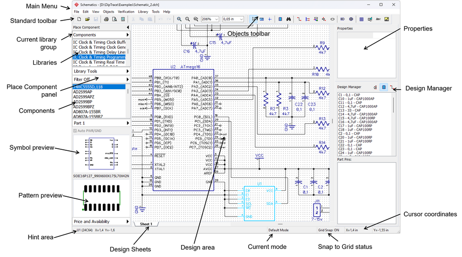
On the design area you can create and edit schematic objects (components, wires, buses, shapes, tables, etc.).
Access all common functions of the program in the main menu. There are the following items: File, Edit, View, Objects, Verification, Library, Tools, Help.
Other interface elements are:
Standard toolbar – tools to work with files, cut/copy/paste objects, print, preview and configure titles, change scale and grid size.
Objects toolbar – default mode, define origin, place components, find components, create and edit wires, buses, page connectors, differential pairs, hierarchy connectors and blocks, place images, shapes, text and tables.
Place Component panel – all standard libraries, user libraries or project components. Select library from the list, find and place component. Set up the library panel, search filters, multi-part component placement tools, symbol and pattern previews.
Properties panel displays the properties of current tool or selected object.
Design Manager navigates you through the schematic (left-click highlights object/s, double click pans the circuit to show selected component or net).
Status Bar shows (left to right) the current hint, mode, snap to grid status and cursor coordinates.
2.1.2. Toolbars
DipTrace Schematic has two instrument toolbars, component placement panel (left side), and the Design Manager (on the right):
Standard Toolbar

New – create a new schematic. If previously opened project is not saved, DipTrace will offer to do that. Only one schematic can be opened in one DipTrace instance, several files – only in several DipTrace Schematics (launched separately). Copy/Paste components between them.
Open – open existing schematic (*.dch) file.
Save – save current schematic into previously selected file. If project has never been saved, the Save as dialog box will pop up.
Print – print current schematic. It is recommended to print from the Preview dialog box. Sheet settings and titles are set in the Titles and Sheet Setup dialog box.
Preview – Preview dialog box pops up.
Titles and Sheet Setup – set sheet size, orientation, border margins, titles, zones in the Titles and Sheet Setup dialog box and edit information blocks in the Title block editor.
Cut – move selected object/s to the clipboard.
Copy – copy selected objects/s to the clipboard.
Paste – paste object/s from the clipboard.
Undo – one editing step backwards.
Redo – one editing step forward. Active only after using the Undo tool. If you edit schematic after using Undo tool, the Redo tool becomes inactive.
Zoom Window – with this tool active, hold down the left mouse button and draw the box to specify where to zoom on the design area.
Zoom Extents – pan schematic to show all objects.
Undo Zoom – return to the previous scale and panning.
Scale (drop-down box) – define schematic scale (from 25% to 800% or manually type in the value). Changing scale is possible with the mouse wheel, plus sign and minus sign default hotkeys and from the main menu.
Grid Size (drop-down box) – select current grid size from the drop-down list or type a new value in the box.
Objects Toolbar

Default Mode – enable default mode. Notice that you can switch to default mode with a right-click or Esc key.
Measure – the ruler tool for measuring any sizes/distances directly on the design area.
Define Origin – define origin with the mouse pointer.
Place Component – Place Component dialog box.
Find Component – Search Component in all DipTrace libraries.
Place Wire – Place Wire tool.
Place Bus – Place Bus tool.
Place Bus Connector – place bus connectors to connect schematic sheets with a bus. To connect two or more bus connectors together, give them the same name.
Edit Mode – edit existing wires and buses. It is activated automatically when you try to edit wire or bus in the Default mode.
Define Differential Pair – create differential pair tool (define positive and negative nets of a pair, change color, net class and review pair properties).
Place Hierarchy Connector – this connector means pin (in/out) of the hierarchical block on a regular sheet.
Place Hierarchy Block – place hierarchical block on the sheet.
Place Table – place table to the schematic sheet.
Place Shape, Text, Picture – these tools allow the user to place the following objects: Line, Arc, Rectangle, Filled Rectangle, Obround, Filled Obround, Polyline, Filled Polygon, Text, Image.
2.1.3. Place Component panel
|
Place Component panel allows the user to select, find and place components on the design area. This panel consists of two lists, four buttons, a checkbox, and preview fields below.To adjust the width of the Place Component panel, hover the mouse pointer over its edge, then drag and drop it. To resize the panel using preset parameters, right-click on it and select preferred option (Small, Medium, Large) or customize the width.
Library list
Select library from the list and all components from the library will be available in the component list right below.
Library Setup – add/delete libraries to/from the library groups, add/delete library groups.
Component list
Displays all the components of the selected library. Select a component from the list and place it directly on the design area. Previews show the symbol and the pattern of selected component.
Hide the Place Component panel by pressing an arrow at the top of the panel.
More information in the Library Setup section of this Help document.
|
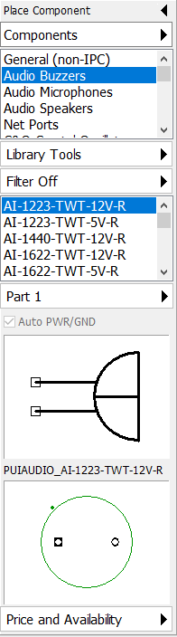
 – select whether you want to place all parts of a
2.1.4. Design Manager
Design Manager panel is on the right side of the screen. Select "View \ Toolbars \ Design Manager" from the main menu or press default Ctrl+2 hotkeys to display/hide the panel. Design Manager consists of the Properties panel and the Design Manager itself to navigate through the schematic.
The Properties panel shows the properties of selected object or active tool and allows the designer to change them.
Right below is the Design Manager, it is the list of all project components (press the  button) or nets (press
  ). Select component or net in the list, and all pins of selected object will appear in the list right below. Left-click in the list to highlight an object, or double click it in the list to pan the design area to selected object.
|
|
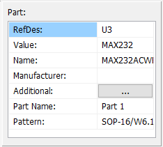
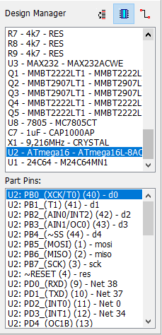
To adjust the width of the Design Manager panel, hover the mouse pointer over its edge, then drag and drop it.
2.1.5. Status Bar
Status bar is located in the bottommost part of the Schematic window.

It shows the following information:
Hint - standard hint containing information about the selected object on the design area.
Mode - shows the current mode (Default, Place Wire, Place Bus, etc.).
Grid Snap - the current Snap to Grid status.
X, Y - coordinates of the current position of the cursor or selected element.
2.1.6. Main menu
2.1.6.1. File
New – create a new schematic. If previously opened project is not saved, DipTrace will offer to do that. Only one schematic can be open in one DipTrace instance, several files – only in several DipTrace Schematics (launched separately). Copy and paste components between them.
Open – open existing schematic (*.dch) file.
Open Recent – open last five schematic projects.
Save – save current schematic into previously selected file. If project has never been saved, the Save as dialog box will pop up. This tool is active only if current schematic has unsaved changes.
Save as – specify the filename and location where schematic file will be saved.
Save Selected As – save selected objects into a separate (*.dch) file.
Import – import schematic from DipTrace ASCII, DipTrace XML, Altium ASCII, P-CAD ASCII, P-CAD PDIF, PADS SCH ASCII 2005, OrCAD EDIF, Eagle XML and KiCAD Schematic formats.
Export – export schematic to DipTrace ASCII, DipTrace XML, P-CAD ASCII, DXF, Eagle XML; DipTrace creates netlists of various formats, Spice netlist for external simulation and Bill of Materials.
Titles and Sheet Setup – open Titles and Sheet Setup dialog box to set sheet size and orientation, border margins, titles etc. Launch the Title Block Editor from this menu item to create custom title blocks.
Preview – open the Preview dialog box before printing.
Print – print current schematic as it is. We recommend to print from the Preview dialog box. Sheet settings and titles are customized in the Titles and Sheet Setup dialog box.
Schematic Information – general information about current circuit (number of pins, parts, components, nets, sheets).
Convert to PCB – open current schematic in the PCB Layout.
Back Annotate – update RefDes, Value, component names, net names, and net classes from the PCB file.
Recover Schematic – recover the latest project. The function is useful if DipTrace closed incorrectly or if the project was not properly saved. DipTrace automatically saves every 10 editing steps.
Recovery Options – configure recovery options: turn ON/OFF recovery and change the number of steps remembered.
Exit – close the Schematic. If current project was not saved, the software will offer to save it.
2.1.6.2. Edit
Undo – one editing step backward.
Redo – one editing step forward. It is active only after using the Undo tool. If you edit schematic after using the Undo, Redo tool becomes inactive.
Undo/ Redo Zoom – select if to consider Zoom a separate editing step or not.
Cut – move selected object/s to the clipboard.
Copy – copy selected object/s to the clipboard.
Paste – paste object/s from the clipboard.
Delete – delete selected object/s.
Select All – select all objects of the schematic.
Edit Selection – selecting objects by type and properties. Different selection modes available: new selection, add to selection, remove from selection, keep selected.
Cross Selection - enable cross selection between Schematic Capture and PCB Layout, choose objects and actions to be included in this function.
Find in Schematic – find specific component or net on the schematic. Search by name, RefDes, value, pattern, etc.
Add Sheet – add new blank sheet to the schematic.
Sheet Type – select whether current sheet is normal or hierarchical.
Copy Matrix – create a copy matrix, based on selected objects. It is possible to specify the number of rows, columns and row/column spacings.
Rotate – rotate selected object/s 90 degrees counter-clockwise. If objects form a group, they have a common center of rotation, otherwise, each has its own center of rotation.
Rotate Group – rotate selected objects around one common center point.
Flip Group – flip selected objects vertically and horizontally.
Align Objects – align selected objects horizontally or vertically and distribute them equally.
Group – unite all selected objects into a group. This tool is active only if several objects are selected.
Ungroup – ungroup selected objects. This tool is active only if one or more groups are selected.
Lock Selected – lock moving and editing of all selected objects.
Unlock Selected – unlock moving and editing of all selected objects, if they were previously locked.
Properties – open the Properties dialog box for selected object.
2.1.6.3. View
Toolbars – show/hide the toolbars.
Display Hint – display hint for the objects on the design area. Hint is duplicated in the bottom-left corner of the screen on the status bar.
Part Preview – preview component before placing it on the schematic.
Group Similar Parts – similar parts of multi-part component are shown with a single item in the part selection list on the Place Component panel. If this option is active, one of similar parts is selected automatically, based on existing parts of the schematic.
Part Markings – default Part Marking options.
Pin Numbers – show/hide the pin numbers and select their font size.
Move Part Text – use this tool to move component markings.
Connection to Bus – set up the markings of wire-to-bus connections. There are two modes: Net Name – net name is shown, Net Number in Bus – net number in the bus is shown (each bus has its own net numeration). Marking text position and font can be changed.
Net Names – set Vector or TrueType font and choose the desired size. This selection will apply to all net names, except those with custom settings.
Hide Power and Gnd – show/hide Power or Ground parts and nets.
Display Titles – show/hide titles. Sheet settings and titles are set in the Titles and Sheet Setup dialog box.
Display Sheet – show/hide the sheet. Sheet size is set in the Titles and Sheet Setup dialog box.
Scale – define schematic scale (from 25% to 800% or type in a new value). Changing the scale is also possible with the mouse wheel or the Plus sign (+) and Minus sign (-) default hotkeys.
Line Width – change the line width of the wires, buses, tables, titles and set diameter of wire nodes.
Colors – change the color template of the design area and its elements.
Graphics Mode – change the graphics mode of the design area.
Units – change units of measurement (mm, mil, or inches).
Precision – adjust precision rate for project values and the grid.
Display Origin – show/hide the origin.
Define Origin – define origin with the mouse pointer or by coordinates (incremental to existing origin).
Grid – show/hide the grid.
Snap to Grid – enable/ disable snap to grid, when the grid is on.
Grid Size – grid size submenu. Select from different standard and custom sizes.
Customize Grid – add/edit standard grid sizes.
2.1.6.4. Objects
Place Component – Place Component dialog box.
Find Component – Search Filters dialog box.
Search Parts at SnapEDA – search SnapEDA libraries directly from within DipTrace.
New Part Request – place an order to get the required part designed within 24 hours.
Circuit – place wire, bus, bus connector to the schematic or enable the Edit mode for existing wires and buses.
High Speed – define differential pair tool and Differential Pair Manager.
Hierarchy – place hierarchical connectors and blocks.
Net Classes – add/edit/delete net classes to the project. More settings available only in the PCB Layout.
Load Classes – load net classes from previously saved rule file (*.rul) or directly from any layout file (*.dip).
Connection Manager – Connection Manager dialog box.
Place Table – place table to the schematic.
Place Shape – place a shape (line, arc, rectangle, filled rectangle, obround, filled obround, polyline, filled polygon).
Place Text – add a text object to the schematic.
Place Picture – add an image to the schematic.
Drawing properties – change default color and line width for shapes and select default font for text objects. Shapes, pictures and text objects in general are considered as shapes.
Measure – the ruler tool for measuring any sizes/distances directly on the design area.
2.1.6.5. Verification
Electrical Rule Check (ERC) – verifies electrical rules for current schematic and shows errors if there are some.
Electrical Rule Setup – change electrical rules in the dialog box.
Check Hierarchy – hierarchy verification, displays errors in the hierarchy tree structure (closed loops).
2.1.6.6. Library
Library Setup – library setup dialog box allows for complete setup of component placement panel: add/delete component library groups, sort them, and add/delete certain libraries and folders to/from the library groups.
Copy <Library name> Library to another group – copy selected library (selected in the list on the Place Component panel) to another library group.
Open <Library name> Library in Component Editor – open current library (selected in the list on the Place Component panel) in the Component Editor
Add Library to <Library group> – add selected library to current library group.
Move <Library name> Library to Another group – move selected library to another library group.
Remove <Library name> Library from <Library group> – remove selected library from current library group.
Add project libraries from another project – add all libraries from another DipTrace file.
Save Design Cache as library – save auto-generated (virtual) Design Cache library as a regular library.
Clear Design Cache – remove all components from the Design Cache library (does not change the project itself).
Remove <Component name> from the Design Cache – remove selected component from the Design Cache library.
2.1.6.7. Tools
SPICE simulator – launch built-in NGSPICE simulator to check the integrity of your circuit and its behaviour.
RefDes Renumbering – arrange reference designators automatically from the top-left to the bottom-right by rows or by columns.
Component Suppliers – launch Suppliers and Prices from Octopart dialog to check prices and availability of parts for your design from different suppliers.
Plugins - extend the software functionality by running plugins. Comprehensive documentation and plugin examples with source codes are provided.
HotKey Settings – check and customize hotkeys for various tools, actions, and dialog boxes in the Schematic.
Environment Variables – define and manage environment variables.
PCB Layout – launch PCB Layout module.
Component Editor – launch Component Editor module.
Pattern Editor – launch Pattern Editor module.
2.1.6.8. Help
Schematic Help – Schematic Help file.
DipTrace Tutorial – DipTrace PDF step-by-step tutorial, learn how to work in DipTrace on the example circuit.
Getting Started – getting started dialog box with useful software links.
Register – enter the User Name and Registration Key to register your DipTrace edition.
Request Support – DipTrace support portal.
PCB Design Service – request affordable PCB design service from our experienced engineers (online request form).
DipTrace Home Page – DipTrace official website.
About – general information (current version, edition, and software build).
2.1.7. Object submenus
2.1.7.1. Component
Right-click on a component to open this submenu:
Component RefDes – change RefDes of the component. Current RefDes is an item caption.
Optimize RefDes – renumber RefDes of the components to optimize numbers (if some components were previously deleted or renamed).
RefDes Renumbering – arrange reference designators from the top-left to the bottom-right by rows or by columns.
Links – display all links from component's additional fields.
Block Subcircuit – open hierarchy block circuit. Item is visible only for hierarchical blocks.
Lock Selected – lock moving and editing of all selected objects.
Unlock Selected – unlock moving and editing of all selected objects, if they were previously locked.
Disconnect Wires – disconnect all component pins from the wires.
Connect Wires – connect component pins to the wire ends located in the same grid point on the design area.
Attached Pattern – attach pattern to the component. You can attach pattern by selecting it from the pattern library and changing pin numbers.
Pad Signal Delay – define any additional distance that a signal propagates within a component. This value is considered for phase and length tuning.
SPICE Model – open SPICE Model dialog to set up or edit the model of the current component or all the components of the schematic that will be used for simulation.
SPICE: Show Current – open NGSPICE Simulator window with the signal trace displayed on the graph (based on the results of a previously-run simulation).
Replace Part – replace current part with another part from component library.
Save to library – save component into a library file or active library.
Price and Availability – check component price and availability from a featured supplier or all the suppliers from Octopart catalog.
Update from library – update selected parts, components or component type from the library.
Pin Numbers – show/hide pin numbers for selected parts.
Part Origin – show/hide the origin of selected component.
Rotate – rotate selected objects 90 degrees counter-clockwise. If objects form a group, they have a common center of rotation, otherwise, each has its own center of rotation.
Flip – flip component horizontally or vertically.
Change Sheet – move part to selected sheet (if circuit has more than one sheet).
Align Objects – align selected objects horizontally or vertically and distribute them equally.
Snap to Grid – snap selected component to the grid, when the grid is on, but Snap to Grid option is disabled for the overall project.
Cut – move selected object to the clipboard.
Copy – copy selected objects to the clipboard.
Delete – delete selected objects.
Group – unite all selected objects into a group. Tool is active only if several objects are selected.
Ungroup – ungroup selected objects. This tool is active only if one or more groups are selected.
Properties – component properties dialog box.
2.1.7.2. Pin
Right-click on the pin to open this submenu.
Pin Name – change pin name. To start/finish inversion, use the tilde sign key.
Net Name – change net name dialog box. Item is visible if this pin belongs to some net.
Not connected – put "not connected" declaration on the pin. Not connected pin is not considered as an error by ERC if Not Connected option is turned ON.
Delete from Net – delete current pin from the net.
Display Wire – display wire connected to the pin. Item is visible only if wire was hidden.
Add to Net – add current pin to net from the list.
Connection Manager – Connection Manager for the circuit.
Signal Delay – set pin signal delay.
Net Properties – net properties dialog box for the net connected to selected pin.
Pin Properties – pin properties dialog box to change all pin properties and font of pin name.
2.1.7.3. Net
Right-click on a wire to open this submenu:
Net Name – change name of the net. Current name is an item caption.
Display Name – show net name in the design area (separate text object).
Direction Arrows – display direction arrows for selected wires.
Wire Color – change color of the net wire.
Lock Selected – lock moving and editing of all selected objects.
Unlock Selected – unlock moving and editing of all selected objects if they were previously locked.
Add Node – add node to the wire segment.
Hide Wire – hide current wire. All pins that belong to this wire will be connected without wires.
Bus Connection – re-connect wire to the bus. The item is available only for wires connected to buses.
Number in Bus – change net number in the bus. Item is visible if "View \ Connection to Bus \ Net Number in Bus" main menu option is checked.
Connection Manager – launch the Connection Manager.
SPICE: Show Voltage – open NGSPICE Simulator window with the signal trace displayed on the graph (based on the results of a previously-run simulation).
Delete Line – delete wire segment.
Delete Wire – delete wire. Net structure is changed.
Change Sheet – move net to selected sheet (if the circuit has more than one sheet). Net can not be moved if it is connected to non-moving objects.
Snap to Grid – snap the selected net of the pair to the grid, when the grid is on, but Snap to Grid option is disabled for the overall project.
Snap to Grid – snap the selected net to the grid, when the grid is on, but Snap to Grid option is disabled for the overall project.
Cut – move selected object to the clipboard.
Copy – copy selected objects to the clipboard.
Delete – delete selected objects.
Group – unite all the selected objects to a group. This tool is active only if several objects are selected.
Ungroup – ungroup the selected objects. This tool is active only if one or more groups are selected.
Properties – Net Properties dialog box.
2.1.7.4. Differential pair
Right-click on a differential pair wire to open this submenu:
Diff Pair Name – change differential pair name. Current name is an item caption.
Display Name – show differential pair name on the design area (separate text object).
Direction Arrows – display signal direction arrow for selected wire.
Diff Pair Color – change color of the differential pair.
Lock Selected – lock moving and editing of all selected objects.
Unlock Selected – unlock moving and editing of all selected objects if they were previously locked.
Add Node – add node to wire segment.
Hide Wire – hide current wire. All pins belonging to this wire will be connected without wires.
Bus Connection – re-connect wire to the bus. The item is available only for wires connected to buses.
Number in Bus – change net number in the bus. Item is visible if "View \ Connection to Bus \ Net Number in Bus" main menu option is checked.
Connection Manager – launch the Connection Manager.
Delete Line – delete wire segment.
Delete Wire – delete wire. Net structure is changed.
Remove Diff Pair – remove differential pair declaration from the nets of the pair. The nets remain.
Change Sheet – move selected net of the pair to another sheet (if circuit has more than one sheet). Net can not be moved if it is connected to non-moving objects.
Cut – move selected object to the clipboard.
Copy – copy selected objects to the clipboard.
Delete – delete selected objects.
Group – unite all selected objects to a group. This tool is active only if several objects are selected.
Ungroup – ungroup selected objects. This tool is active only if one or more groups are selected.
Properties – Differential Pair Properties dialog box.
2.1.7.5. Bus
Right-click on a bus to open this submenu.
Bus Name – change the name of the bus. Current name is an item caption.
Display Name – show bus name on the design area (separate text object).
Lock Selected – lock moving and editing of all selected objects.
Unlock Selected – unlock moving and editing of all selected objects, if they were previously locked.
Add Node – add node to the bus segment.
Delete Line – delete bus segment.
Delete Wire – delete bus line. Bus structure is changed if necessary.
Change Sheet – change current sheet of selected bus.
Snap to Grid – snap the selected bus to grid, when the grid is on, but Snap to Grid option is disabled for the overall project.
Cut – move selected object to the clipboard.
Copy – copy selected object/s to the clipboard.
Delete – delete selected objects.
Group – unite all selected objects to a group. This tool is active only if several objects are selected.
Ungroup – ungroup selected objects. This tool is active only if one or more groups are selected.
Bus Nets – list of the bus nets. Here you can delete nets from the bus if necessary.
2.1.7.6. Bus connector
Right-click on a bus connector to open this submenu.
Bus Connector Name – change the name of the bus connector. Current name is an item caption. Busses connected to connectors with similar names are automatically merged.
Lock Selected – lock moving and editing of all selected objects.
Unlock Selected – unlock moving and editing of all selected objects, if they were previously locked.
Change Sheet – change current bus connector sheet.
Align Objects – align selected objects horizontally or vertically and distribute them equally.
Snap to Grid – snap selected bus connector to the grid, when the grid is on, but Snap to Grid option is disabled for the overall project.
Cut – move selected object/s to the clipboard.
Copy – copy selected object/s to the clipboard.
Delete – delete selected object/s.
Group – unite all selected objects into a group. This tool is active only if several objects are selected.
Ungroup – ungroup selected objects. This tool is active only if one or more groups are selected.
2.1.7.7. Shape
Right-click on a shape, text, or picture to open this submenu:
Shape Name – change the shape name or the text.
Edit Text – change the text. Object size is changed automatically.
Font Type – choose font type of a text object (Vector, TrueType). Unicode characters are supported in TrueType mode only.
Font – change font settings (size, text width, line width) of a text object.
Lock Selected – lock moving and editing of selected objects.
Unlock Selected – unlock moving and editing of selected objects, if they were previously locked.
Insert Point – insert point to the polyline or polygon.
Delete Point – delete point from the polyline or polygon.
Rotate – rotate selected objects 90 degrees counter-clockwise. If objects form a group, they have a common center of rotation, otherwise, each has its own.
Change Sheet – change current sheet (move shape to another schematic sheet).
Align Objects – align selected objects horizontally or vertically and distribute them equally.
Snap to Grid – snap the selected shape to grid, when the grid is on, but Snap to Grid option is disabled for the overall project.
Cut – move selected object/s to the clipboard.
Copy – copy selected object/s.
Delete – delete selected object/s.
Group – unite all selected objects to a group. This tool is active only if several objects are selected.
Ungroup – ungroup selected objects. This tool is active only if one or more groups are selected.
Font Type – choose the font type for the text object (Vector, TrueType). Unicode is supported only in the TrueType mode.
Font – change text font. It is active only for the text objects.
Properties – change Shape Properties.
2.1.7.8. Table
Right-click on the table to open this submenu.
Name – change table name. Current name is the item caption.
Current Cell – change properties of current table cell (size, text, align, font).
Lock Selected – lock moving and editing of selected objects.
Unlock Selected – unlock moving and editing of selected objects, if they were previously locked.
Column Width – change column width.
Row Height – change row height.
Add Column – add new column to the table.
Add Row – add new row to the table.
Insert Column – insert new column.
Insert Row – inserts new row.
Delete Column – delete current column from the table.
Delete Row – delete current row from the table.
Save to File – save table content to Excel CSV or Text file.
Rotate – rotate selected objects 90 degrees counter-clockwise. If objects form a group, they have a common center of rotation, otherwise each has its own center of rotation.
Change Sheet – move table to another sheet.
Align Objects – align selected objects horizontally or vertically and distribute them equally.
Snap to Grid – snap the selected table to grid, when the grid is on, but Snap to Grid option is disabled for the overall project.
Cut – move selected object/s to the clipboard.
Copy – copy selected object/s.
Delete – delete selected object/s.
Group – unite all selected objects into a group. This tool is active only if several objects are selected.
Ungroup – ungroup selected objects. This tool is active only if one or more groups are selected.
Properties – change table properties.
2.1.8. Modes of operation
There are several modes of operation in the DipTrace Schematic:
Default mode – set by default. It becomes active as soon as you launch the Schematic. To activate this mode from any other mode, you need to right-click on empty space on the design area (maybe several times). Esc key or  button on the Objects toolbar can be used as well. This mode allows the user to select and move objects as well as place wires, edit existing wires, and change size of shapes, texts, and pictures by automatically switching to necessary operational mode after clicking on the object.
Measure mode. Select measuring tool from the main menu ("Objects/ Measure") or press  on the Objects toolbar. Left-click in the starting point and move the mouse pointer to the end point keeping left button pressed. The length will be displayed in the bottom-left corner, in the hint area.
Define Origin mode. Select Define Origin tool from the main menu (View/ Define Origin/ By Mouse Pointer) or press on the Objects toolbar. Left-click in the design area to establish a new Origin point.
Place Component – select component in the component list on the Place Component panel or press Place button in the Place Component dialog box to enable this mode.
Place Table – select "Objects \ Place Table" from the main menu or press  button on the Objects toolbar.
Place Wire – select "Objects \ Circuit \ Place Wire" from the main menu, press button on the Objects toolbar, or simply left-click on the pin to enable this mode. Select the first pin or wire segment, then draw it to the final pin or wire segment, and left-click it. It is possible to place wire automatically or segment by segment.
Place Bus – select "Objects \ Circuit \ Place Bus" from the main menu or press  button on the Objects toolbar. To place bus, select the start point, bus segment, or bus connector, and specify the key points of the bus all the way to the final bus segment or bus connector with the left mouse clicks. Right-click, and choose Enter from the submenu to apply.
Place Bus Connector – select "Objects \ Circuit \ Place Bus Connector" from the main menu or press  button on the Objects toolbar. To place bus connector, just left-click on the design area. Give similar names to several bus connectors to connect them. All buses will be united automatically.
Edit Wires and Buses – select "Objects \ Circuit \ Edit Mode" from the main menu, press  button on the Objects toolbar or simply drag and drop. This mode allows the designer to move wire segments and bus segments orthogonally.
Place Shape – select shape or text placement tool from the main menu ("Objects") or  button on the Objects toolbar.
Place Text mode. Select text placement tool from the main menu (Objects/ Place Text) or press  button. Left-click on the design area and type a text. DipTrace supports multi-line text placement. Select Edit Text item from the right-click submenu to change the text, line spacing and alignment. Use Text Properties dialogue, launched by selecting Properties item from the right-click submenu, to adjust other text properties: font, layer, text angle, anchor point location, etc.
Move Part Markings – select "View \Move Part Texts" from the main menu or press F10 default hotkey. Press R or Space to rotate texts while moving, just like regular objects.
2.1.9. Hotkeys
DipTrace features customizable hotkeys in all software modules. To open the Hotkey Settings dialog box, proceed to "Tools/ Hotkey Settings" from the main menu in any of the DipTrace modules: Schematic, PCB Layout, Component and Pattern Editors. The designer can view or assign hotkeys to various tools, actions and dialog boxes by left clicking in a corresponding field and pressing a keyboard combination.
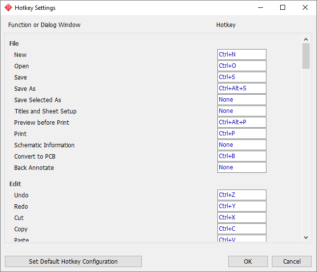
If a combination is already in use, a warning message comes out. Notice that certain shortcuts are reserved by the program and are not customizable. Press OK to apply changes. To restore default configuration, press Set Default Hotkey Configuration button on the panel.
Hotkeys reserved by the system:
Ctrl Shift Shift + mouse Enter Esc Left arrow Right arrow Up arrow Down arrow Shift + S Shift+I Shift+P Alt+any key |
– hold down to invert selection; – hold down to add objects to selection; – orthogonal moving of selected objects; – complete action; – cancel action; – move object left, pan left while routing/building; – move object right, pan right while routing/building; – move object up, pan up while routing/building; – move object down, pan down while routing/building; – enable disable auto-panning; – ON/OFF automatic check for new DipTrace versions; – reserved by the system; – reserved by the system. |
Please notice that most items in the main menu and various drop-down lists have shortcut combinations right next to them. In this help document we always refer to default shortcuts.
2.1.10. Environment Variables
According to DipTrace License Policy, the software can be used by one license holder on several devices. To ensure smooth portability of your projects, DipTrace features an Environment Variables tool that allows setting variables for the paths to directories containing libraries, 3D models, images, etc. on different machines.
Go to Tools/ Environment Variables to open the Environment Variables dialog.
In the Common Variables section you can see the paths used by the software during installation and the corresponding variables for those paths.
In the User Variables part you can establish new variables for the paths to the directories, where your libraries or 3D models are stored. Type the variable in the Variable cell and set the path in the Folder line or press  button and select Browse for Folder to select the directory. Use the same variable on another PC to associate it with the path to the required folder on that machine. In this way when switching between machines the software will look for the files using the path corresponding to the established variable on the given PC.
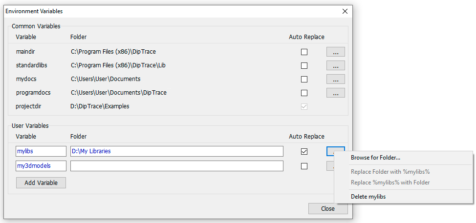
You can check the Auto Replace option for the software to substitute the path with the variable in any items with such path as soon as they appear in the project or press button and select “Replace folder with %variable name%” to apply this command to all currently existing items in the project. To reverse the command select “Replace %variable name% with Folder” from the menu.
Remember to use the same variables to set the paths to the corresponding folders on another machine. If your component or 3D model libraries have been changed, make sure to update them in the source folder on your device.
To delete a variable press and select Delete <Variable Name>.
Environment Variables feature also allows creating a portable version of the program by establishing a variable for the launch directory, which can be stored, for instance, on a portable drive.
2.2. Working with files
2.2.1. Create project
If you launch DipTrace (no command prompt), a new project will be created automatically. To create a new project, select "File \ New" from the main menu or press the corresponding button on the Standard toolbar. If current project is not saved, the program will offer to do this.
2.2.2. Open project
Select "File \ Open" from the main menu or press the corresponding button on the Standard toolbar to open schematic file and choose the file you need (*.dch).
The last five files are saved in the "File \ Open Recent" submenu for quick access.
2.2.3. Save project
It is possible to save the project by choosing "File \ Save" or "File \ Save as" from the main menu. For the first item there is a tool on the Standard toolbar.
To save project, select "File \ Save" from the main menu or press the corresponding button on the Standard toolbar. If schematic has never been saved, the Save As dialog box will pop up automatically. The user should select the location and file name for the schematic, all further changes will be automatically rewritten into this file.
If you need to save only a part of your schematic, select it, and go to "File \ Save Selected As" from the main menu.
2.2.4. Schematic to PCB
To convert existing schematic to PCB Layout, select "File \ Convert to PCB" from the main menu. You can also save your schematic and open a *.dch file directly in the PCB Layout.
When you open schematic in the PCB Layout, DipTrace suggests to use schematic rules or load rules from another layout project (layers, DRC, net classes, via styles etc.). You can also arrange components for easier placement. Choose "Placement \ Arrange Components" from the main menu in the PCB Layout.
2.2.5. Back Annotate
Back annotate feature allows the user to automatically apply changes made in the PCB Layout directly on the principal circuit in the Schematic.
This feature has limited functionality (only updates the reference designators, values and types of components, net names, and net classes) and is not capable to add new components or create new nets on the principal circuit.
We always recommend that any changes should be made in the schematic first. Back Annotation does not work if schematic or PCB layout has been created in different PCB CAD software.
To launch the back annotation for existing schematic, select "File \ Back Annotate" from the main menu, then select the PCB layout file (*.dip).
Back annotation of the names does not work for multiple hierarchical blocks (if any hierarchical sheet was placed more than once). In this case names on the PCB and Schematic will be different (R1 in Schematic will be R1_1, R1_2, etc. in the PCB Layout, due to hierarchy block index in the component RefDes on the board).
2.2.6. Import
2.2.6.1. DipTrace ASCII
DipTrace allows the user to save/open data in the textual ASCII format. This format has been developed to allow for data transferring from/to other EDA packages and for forward compatibility.
To import schematic file from DipTrace ASCII format, select "File \ Import \ DipTrace ASCII", choose a file, and click Import.
2.2.6.2. DipTace XML
DipTrace Schematic Capture allows saving/ opening data in the textual DipTrace XML format. This format can be used for data transferring from/to other EDA packages and for forward compatibility between the DipTrace versions.
To import a library file in DipTrace XML format, select "Library/ Import/ DipXML" then select file, and click OK.
2.2.6.3. Altium ASCII
DipTrace imports schematics from the Altium ASCII (*.schdoc) format.
Notice that your schematic should be in the ASCII format, not binary (save schematic as an ASCII file in the Altium software).
In the DipTrace select "File \ Import \ Altium ASCII" from the main menu and open Altium ASCII schematic file. The following dialog pops up:
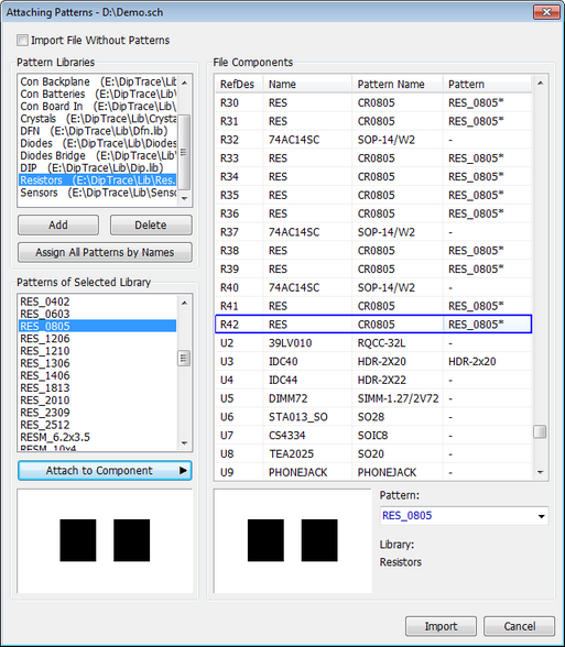
Schematics include only pattern names, you need to specify where to get the pattern libraries to proceed. Use Add and Delete buttons to add pattern libraries to the list. With Shift or Ctrl keys several libraries can be added at a time.
We recommend importing your Altium ASCII pattern libraries (*.lia) in the Pattern Editor prior to importing schematic or PCB files from Altium, but you can also find patterns in the DipTrace libraries. Use Pattern Names Help to quickly find acceptable component footprints in DipTrace standard libraries because pattern names may be different.
Press Assign all Patterns by names – patterns will be found and attached automatically. Check all patterns yourself, use File Components list and the preview field below.
File Components list
RefDes – Altium component reference designator;
Name – Altium component name;
Pattern Name – Altium pattern name;
Pattern – related DipTrace pattern.
Select component in the list, then select pattern from the library, and press Attach to Component button to attach patterns to components according to component RefDes, name or pattern name.
The star symbol (*) after the pattern name in the list means that this pattern had been connected manually.
You can also import Altium schematic without patterns.
2.2.6.4. Eagle Schematic
DipTrace imports schematics from the EAGLE format (*.sch).
Select "File \ Import \ EAGLE Schematic" from the main menu in the DipTrace Schematic, and select an EAGLE schematic file (*.sch).
Components and patterns are included into EAGLE schematic and PCB files, you don't have to connect patterns when importing from EAGLE. All components of an imported project are available in the auto-generated Design Cache library in the Project Libraries library group on the Place Component panel. You can save Design Cache as a regular library directly on the Place Component panel or import component and pattern libraries from EAGLE in DipTrace Component Editor and DipTrace Pattern Editor.
2.2.6.5. EasyEDA Pro
DipTrace supports import of schematics from EasyEDA Pro format (*.epro).
Choose "File \ Import \ EasyEDA Pro" from the main menu in the DipTrace Schematic, and select EasyEDA Pro Project file (*.epro).
2.2.6.6. P-CAD ASCII
DipTrace imports schematics from the P-CAD ASCII (*.sch) format.
Notice that your schematic should be in the ASCII format, not binary (both have the same extension in P-CAD).
Select "File \ Import \ P-CAD ASCII" from the main menu and open schematic file. The following dialog pops up:
Schematics include only pattern names, you need to specify where to get the pattern libraries to proceed. Use Add and Delete buttons to add pattern libraries to the list. With Shift or Ctrl keys several libraries can be added at a time.
We recommend importing your P-CAD ASCII pattern libraries (*.lia) in the Pattern Editor prior to importing schematic or PCB files from P-CAD, but you can also find patterns in the DipTrace libraries. Use Pattern Names Help to quickly find acceptable component footprints in DipTrace standard libraries because pattern names may be different.
Press Assign all Patterns by names – patterns will be found and attached automatically. Check all patterns yourself, use File Components list and the preview field below.
File Components list
RefDes – P-CAD component reference designator;
Name – P-CAD component name;
Pattern Name – P-CAD pattern name;
Pattern – related DipTrace pattern.
Select component in the list, then select pattern from the library, and press Attach to Component button to attach patterns to components according to component RefDes, name or pattern name.
The star symbol (*) after the pattern name in the list means that this pattern had been connected manually.
You can also import P-CAD schematic without patterns.
2.2.6.7. P-CAD PDIF
DipTrace Schematic module allows the user to import P-CAD PDIF files.
Select "File \ Import \ P-CAD PDIF" from the main menu, then select *.pdf or *.cfg file of a P-CAD Schematic. *.cfg files are used for multi-sheet schematics.
Notice that P-CAD has separate *.pdf file for each sheet and *.cfg file to unite all schematic sheets together. DipTrace has a single *.dsc file for single or multi-sheet schematics.
You can import schematic without patterns.
Notice that importing P-CAD PDIF schematic does not differ from importing other formats. See P-CAD ASCII import page for basic instructions.
Use Pattern Names Help to quickly find acceptable component footprints in DipTrace standard libraries.
2.2.6.8. PADS ASCII 2005
DipTrace imports schematics from the PADS Schematic ASCII 2005 (*.txt) format. Select "File \ Import \ PADS SCH ASCII 2005" from the main menu and open a schematic file. The following window pops up:
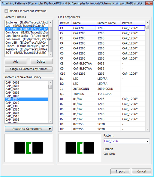
PADS schematics include only pattern names, you need to specify where to get the pattern libraries to proceed. Use Add and Delete buttons to add pattern libraries to the list. With Shift or Ctrl keys several libraries can be added at a time.
We recommend importing your PADS ASCII pattern libraries (files with *.d and *.c extensions) in the Pattern Editor prior to importing schematic or PCB files from PADS, but you can also find patterns in the DipTrace libraries. Use Pattern Names Help to quickly find acceptable component footprints in DipTrace standard libraries because pattern names may be different.
Press Assign all Patterns by names – patterns will be found and attached automatically. Check all patterns yourself, use File Components list and the preview field below.
File Components list
RefDes – PADS component reference designator;
Name – PADS component name;
Pattern Name – PADS pattern name;
Pattern – related DipTrace pattern.
Select component in the list, then select pattern from the library, and press Attach to Component button to attach patterns to components according to component RefDes, name or pattern name.
The star symbol (*) after the pattern name in the list means that this pattern had been connected manually.
You can also import PADS schematic without patterns.
2.2.6.9. OrCAD EDIF
DipTrace imports schematics from the OrCAD EDIF format.
Select "File \ Import \ OrCAD EDIF Schematic" from the main menu and open schematic file (file with *.edf extension). The following window pops up:
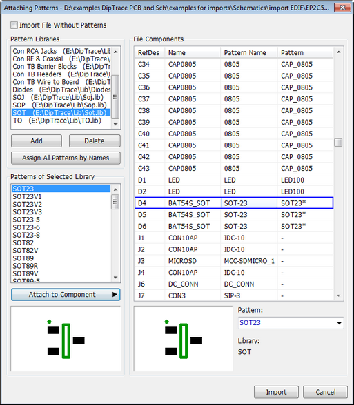
OrCAD schematics include only pattern names, you need to specify where to get the pattern libraries to proceed. Use Add and Delete buttons to add pattern libraries to the list. With Shift or Ctrl keys several libraries can be added at a time. Use Pattern Names Help to quickly find acceptable component footprints in DipTrace standard libraries because pattern names may be different.
Press Assign all Patterns by names – patterns will be found and attached automatically. Check all patterns yourself, use File Components list and the preview field below.
File Components list
RefDes – OrCAD component reference designator;
Name – OrCAD component name;
Pattern Name – OrCAD pattern name;
Pattern – related DipTrace pattern.
Select component in the list, then select pattern from the library, and press Attach to Component button to attach patterns to components according to component RefDes, name or pattern name.
The star symbol (*) after the pattern name in the list means that this pattern had been connected manually.
You can also import OrCAD schematic without patterns.
2.2.6.10. KiCAD Schematic
DipTrace imports schematics from the KiCAD Schematic format.
Select "File \ Import \ KiCAD Schematic" from the main menu and open schematic file (file with *.pro extension). The following window pops up:
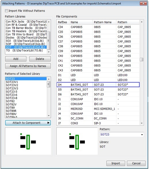
KiCAD schematics include only pattern names and you need to specify where to get the pattern libraries to proceed. Use Add and Delete buttons to add pattern libraries to the list. With Shift or Ctrl keys several libraries can be added at a time. Use Pattern Names Help to quickly find acceptable component footprints in DipTrace standard libraries because pattern names may be different.
Press Assign all Patterns by names – patterns will be found and attached automatically. Check all patterns yourself, use File Components list and the preview field below.
File Components list
RefDes – KiCAD component reference designator;
Name – KiCAD component name;
Pattern Name – KiCAD pattern name;
Pattern – related DipTrace pattern.
Select component in the list, then select pattern from the library, and press Attach to Component button to attach patterns to components according to component RefDes, name or pattern name.
The star symbol (*) after the pattern name in the list means that this pattern had been connected manually.
You can also import KiCAD schematic without patterns.
2.2.6.11. Pulsonix
DipTrace supports import of schematics from Pulsonix format (*.psa).
Choose "File \ Import \ Pulsonix" from the main menu in the DipTrace Schematic, and select Pulsonix schematics file (*.psa).
2.2.7. Export
2.2.7.1. DipTrace ASCII
DipTrace allows you to save/open data in textual ASCII format. This format has been developed to allow for data transferring from/to other EDA packages and for forward compatibility.
To export schematic file into DipTrace ASCII format, select "File \ Export \ DipTrace ASCII", define the filename, and press OK.
2.2.7.2. DipTace XML
DipTrace Schematic Capture allows saving/ opening data in the textual DipTrace XML format. This format can be used for data transferring from/to other EDA packages and for forward compatibility between the DipTrace versions.
To export a schematic file in DipTrace XML format, select "Library/ Export/ DipXML" then define filename, and click OK.
2.2.7.3. DXF
DipTrace allows for exporting schematic to DXF format accepted by almost all PCB CAD programs. Select "File \ Export \ DXF" from the main menu. The following window pops up automatically:
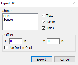
Select schematic sheet for exporting and enable/disable text, tables, and titles in the DXF file. Other objects will be exported as they are. Change coordinate offset or use the design origin. Press Export and define the filename to complete the export process or press Cancel to reject it.
2.2.7.4. P-CAD ASCII
DipTrace allows the user to export Schematics to P-CAD ASCII format (files with *.sch extension).
To export existing schematic to P-CAD, select "File \ Export \ P-CAD ASCII" from the main menu, define the filename and save it.
2.2.7.5. Netlist
DipTrace allows the designer to export schematic's netlist in the most popular netlist formats. Netlists allow for transferring the source data to various board design applications. DipTrace exports netlists of these formats: Accel, Allegro, KiCAD, Mentor, OrCAD, PADS, P-CAD, Protel 2.0, Tango.
To export a netlist, select "File \ Export \ Netlist" and choose appropriate netlist format. In the pop-up dialog box, define the filename for the netlist, and press OK.
2.2.7.6. Eagle Schematic
DipTrace allows the user to export Schematics to Eagle Schematic format (files with *.sch).
Please note that in DipTrace, both Pin Name and Pin Number can be assigned to a pin, while in Eagle a pin is denominated only with a Pin Name. When exporting DipTrace Schematic to Eagle format, Pin Name, if assigned in the source file, is carried over to Eagle. However, if no Pin Name is assigned in the original project, Pin Number is carried over to Eagle as a Pin Name.
Pin Number display is configured for all pins of all components via View/ Pin Numbers item (in Eagle: Pin Settings - Visible/ Pad).
To export existing schematic to Eagle, select "File \ Export \ Eagle Schematic" from the main menu, define the filename and save it.
2.2.7.7. SPICE netlist
You can run SPICE simulation directly in DipTrace or export SPICE netlist (*.cir) for external simulation.
We can recommend freeware LT Spice software from the Linear Technologies to simulate schematics made in DipTrace.
To export SPICE netlist from DipTrace Schematic, select "File \ Export \ Spice Netlist" from the main menu.
In the pop-up dialog box specify GND net (zero signal), SPICE commands, and press OK to export the netlist.
SPICE models for all components should be defined before export.
Simulation command for LT Spice looks like this: ".TRAN 0s 10s 0.1s", where 0s – start time, 10s – end time, 0.1s – step of simulation.
However, correct start/end time and step can be changed directly in the LT Spice. Please refer to the corresponding SPICE language documentation.
2.2.7.8. Bill of Materials
To create a bill of materials for the schematic, select "File/ Export/ Bill of Materials" from the main menu. The following dialog box will pop up:
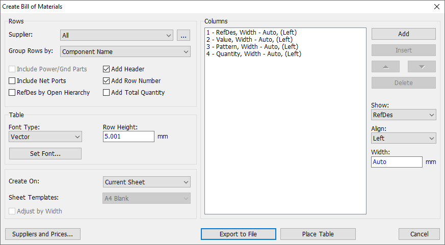
The rows of the BOM table can be grouped by components, parts, component name, name and value/ pattern. Select the appropriate option from the Group Rows by drop-down list.
Reference designators for multiple hierarchical blocks may correspond to schematic (R1, R2, etc.) or PCB (R1_1, R1_2, etc., R2_1, R2_2, etc.). Quantity is always counted by the number of physical components (by PCB). To show RefDes by opened hierarchy, check RefDes by Open Hierarchy option.
To show column headers, check Add Header item.
Check Add Row Number to add the first column with row numbers ("1", "2", "3", etc.)
Check Add Total Quantity to add the last row with total quantity of components, parts, pins (depending on the row).
You can define the columns of the BOM table.
To add a column, select component property from the Show drop-down list, set the column width, alignment, and press Add button. Remember to add Supplier and Price columns, if you want this information to be included into the BOM table.
You can press the Suppliers and Prices button in the bottom-left corner to open Suppliers and Prices from Octopart dialog and assign suppliers or check the current prices.
To change parameters of the existing column, select it from the Columns list, and change the corresponding fields.
To insert a new column, select position in the Columns list, and press Insert button.
To delete a column, select it from the Columns list, and press Delete button.
There are four ways to create a BOM table:
1. Current Sheet. Only one table with all components. To place it, select Current Sheet from the Create On drop-down list, press Place Table, and left-click the top left corner of the table on the schematic sheet.
2. Each Sheet. Each sheet of schematic has its own bill of materials. To create BOM tables, select Each Sheet from the Create On list, press Place Table, and left-click the top-left corners of the BOM tables on every schematic sheet. The tables are created on all schematic sheets. You can move the BOM tables directly on the sheets, like regular table objects.
3. New Sheet(s). DipTrace creates a new sheet and places the BOM table there. You can select the sheet template from the template list and adjust table by sheet border width. Press Place Table, the BOM table will appear according to the sheet size and titles. If there is no space to place all components on a single sheet, the software will add more sheets automatically.
4. Export to File. The BOM files are available in 2 formats: Excel CSV and files with *.bom extension. When exporting to file, DipTrace will ask you to set a Column Divider and decide whether to use Quotation Marks for values or not.
Please notice that you can add custom rows and columns to the BOM file in any spreadsheet editor.
2.2.8. Schematic information
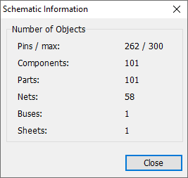
With Schematic Information dialog box you can check the number of components, pins, nets, etc.
To show this dialog box, select "File/ Schematic Information" from the main menu.
2.3. Working with libraries
2.3.1. Review
In DipTrace a typical electronic component consists of schematic symbol, PCB footprint (pattern), and possibly a 3D model. All these entities represent a single component on various design stages. The Schematic module works with schematic symbols, which represent real electronic components on the principal circuit.
Refer to the Component Editor Help and Pattern Editor Help for more details about designing components and libraries.
Place Component panel is on the left side of the screen. It has all necessary tools for placing single- and multi-part components and managing libraries and library groups in all DipTrace modules.
Libraries are organized to library groups for convenience.
There are three library groups available by default:
1) Components (all standard libraries, user can not edit this library group);
2) User Components (designer adds/deletes libraries to/from this group);
3) Project Libraries (auto-generated library with all components from currently opened circuit).
Library Setup dialog box allows the user to add libraries from separate files into the DipTrace system, create new and edit existing library groups. Changes in the library structure made in the Schematic immediately affect the libraries in the PCB Layout and other software modules. Pattern library groups are not visible on the panel in the Schematic.
It is possible to search components in any library or all of them by applying search filters. Select "Objects/ Find Component" from the main menu or press  button on the Place Component panel to set up and apply the filters. You can stop the filter at any moment of the search process.
2.3.2. Library groups
Library groups are very easy means of organizing libraries. There are three default library groups: Components, User Components, and Project Libraries (auto-generated library group for storing all components of active principal circuit in the Design Cache library).
Press  to change active library group or open the Library Setup dialog box to create and edit library groups and connect separate libraries from the files.
Press  to change move/copy/delete component libraries between the library groups.
2.3.3. Library setup
Place Component panel allows the user to find and place components. Select the library group, then select library from the list, and select the component from the list right below to place it on the design area.
Library Setup
Go to "Library \ Library Setup" from the main menu or press and select Library Setup from the submenu. In the pop-up dialog box the user can create library groups and add/delete libraries to/from the groups. The Library Setup panel is the same as in the PCB Layout and allows the user to edit not only the component library groups, but the pattern library groups as well.
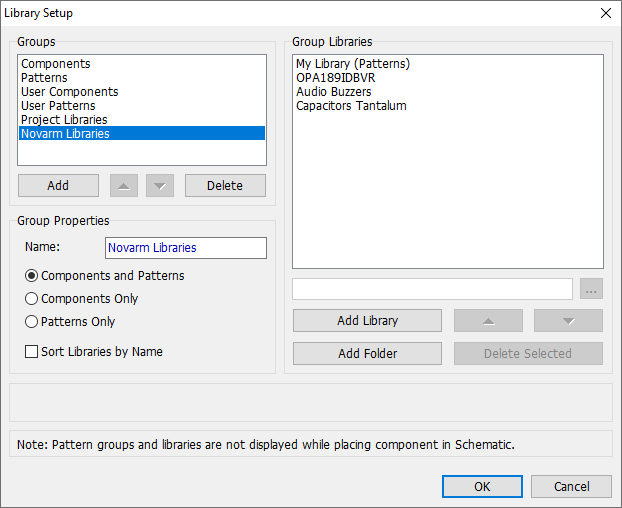
Press Add to create new library group, type in its name into the field below, and select the group type, depending on what libraries you are going to store in the group:
Components Only type allows for adding only component libraries (files with *.eli extension) to the group;
Patterns Only type allows for adding only pattern libraries (files with *.lib extension);
Components and Patterns type allows for adding both library files into current library group.
Select library group from the list, and press Add Library or Add Folder buttons to add libraries from the files to the library group.
The user can not edit the standard library groups: Components and Patterns.
2.3.4. Search filters
Search filters help to find components by various parameters. Select "Objects \ Find Component" from the main menu or press button on the Place Component panel. Select the search area (where to search for components), type in the name, and press Apply Filter. Press + or - buttons to add/delete new filters, which allow for finding components by RefDes, Value, Manufacturer, Pattern, Datasheet or Additional Fields.
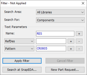
Press Search at SnapEDA button to open SnapEDA dialog and look up the components based on the entered parameters in SNapEDA libraries directly from within DipTrace.
Press New Part Request to be directed to the 24-Hour Component Design Service, where you can place an order for the required component design.
2.3.5. Search at SnapEDA
To look for the required components in SnapEDA libraries, go to "Objects \ Search Parts at SnapEDA". In the pop-up, register or log-in, if necessary, then enter data in the Search field and press  button.
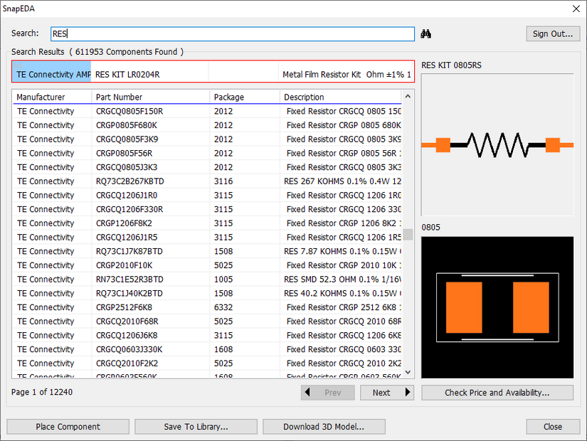
Select a component from the search results, its symbol and pattern will appear in the preview field, if available.
Press Place Component button to place the pattern directly on the design area.
Save to Library button allows adding the component to the existing user library or a newly-created one.
Download 3D Model button gets active, if a 3D model is available for the selected component. Press it to download the .step file to your computer. The model will be automatically attached to the respective pattern.
Press Check Price and Availability button and choose the option that suits you best. If <Featured Supplier> is selected - you will be directed to its official website.
With Check All Suppliers option selected, you’ll be able to check prices and availability of the selected component from different suppliers listed in Octopart catalog.
Note that Digi-Key is a featured supplier by default, you can change it as well as your preferred currency by pressing the Featured Supplier and Currency button at the bottom of the Suppliers and Prices from Octopart dialog.
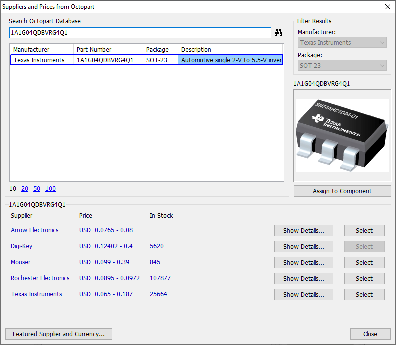
2.3.6. Save components as a library
DipTrace Schematic module allows the designer to save components of the current principal circuit as a new library or add them to the existing one. Select components on the design area, right-click on one of them, and choose Save To Library from the submenu.
Design Cache (auto-generated library with all components of the design) can be saved as well – select Design Cache library, press , then select Save Design Cache as Library from the submenu.
2.4. View functions
2.4.1. Toolbars
DipTrace Schematic has two toolbars, Design Manager, and Place Component panel.
To show/hide the toolbars and panels, select "View \ Toolbars" from the main menu (or use Ctrl+1 – Ctrl+4 default hotkeys). The user can increase the size of the design area by hiding unused toolbars or panels. DipTrace remembers the configuration of the toolbars.
2.4.2. Group similar parts
Multi-part components typically consist of several identical parts and a power part. DipTrace allows the designer to group similar parts of the multi-part component for convenience.
If "View \ Group Similar Parts" main menu item is checked, all similar parts are shown by a single item in the list of component parts on the Place Component panel.
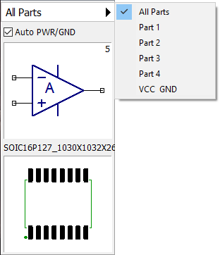
The part for placement is selected from a group automatically depending on existing parts on the schematic.
If "View \ Group Similar Parts" is unchecked you can select any of similar parts manually.
Notice that this feature works only for similar parts. If some multi-part component has different parts (even if they are visually identical) Grouping Similar Parts does not work.
2.4.3. Part Markings
To define default Part Markings settings for the current project, select "View/ Part Markings" from the main menu. Mark the parameter/s you would like to be shown: RefDes, Name, Values, Manufacturer, Datasheet or any additional field of the component.
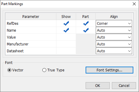
If you are dealing with a multi-part component, you can also choose to show individual parameters of the parts.
Component markings can be aligned by center, top, bottom, left, right, top-right corner of the part or automatically (i.e. the software will select the best way to position the markings).
In this dialogue, you can also change font type (Vector or TrueType). We strongly recommend using Vector font and switch to the TrueType if you need Unicode characters.
Press Font Settings button to adjust markings font size, line and text width and text color.
To move component markings, select "View/ Move Part Texts" from the main menu or press F10 hotkey (by default).
To rotate markings, press R or Space while moving them.
To see how to set up display of markings for individual components, check Component Properties section of this Help manual.
2.4.4. Pin numbers
Configure pin number display options for all schematic parts or for each component individually. Custom settings have priority over the default (common) settings.
To show/hide pin numbers for all components, select "View \ Pin Numbers" from the main menu. You can change the font type and size here too.
For individual settings select the component/s, right-click on one of them, and choose Pin Numbers. It is possible to use default settings for schematic or show/hide pin numbers for particular components.
2.4.5. Connection to Bus
When a wire is connected to the bus, the connection point is marked with the net name or net number (in the bus). The marking can be above the wires or below them.
To configure what to display and where to display it, select "View \ Connection to Bus" from the main menu.
Here you can also define the font type and the size for bus markings.
DipTrace automatically assigns the net numbers in the bus (you can rearrange them). Right-click on the wire near the bus connection, and select Number in Bus from the submenu. This item is visible only if "View \ Connection to Bus \ Net Number in Bus" main menu item is checked.
2.4.6. Net Names
Use the Net Names option under the View menu to configure a common font type and size for the names of all schematic nets.
To display a net name, right-click on a net and select Display Name.
For individual net name settings, right-click on the net name box and choose one of the following options:
Edit Text: Modify the text, line spacing, angle, and anchor point.
Type: Set the font to either Vector or TrueType.
Font: Adjust the size, line width, text width, and color.
Keep in mind that custom settings for individual nets take precedence over the common settings.
2.4.7. Power and GND
It is possible to hide Power and Ground parts and nets. Choose "View \ Hide Power and Gnd" item from the main menu.
Use Net Properties dialog box to change net settings.
2.4.8. Titles
To show/hide titles and sheet, select "View \ Display Titles" and "View \ Display Sheet" from the main menu.
Sheet size and orientation, border margins, zones, and title blocks are specified in the Sheet and Titles Setup dialog box. Select "View \ Sheet and Titles Setup" from the main menu or press  button on the Standard toolbar. To create custom title blocks, press the Title Block Editor button in the Sheet and Titles Setup dialog box.
To change text, font, and alignment of title block field, move the cursor to the corresponding field, and left-click it.
To show/hide the borders of the sheet on the design area, select "View \ Display Sheet" from the main menu.
2.4.9. Scaling/Panning
There are several ways to change the scale of the design area:
1. The mouse wheel – you can decrease or increase scale in very wide limits.
2. Drop-down list on the Standard toolbar (from 25% to 800%).
3. "View \ Scale" from the main menu. It is possible to select from 25% to 800%, zoom in, zoom out or specify custom scale.
4. Plus sign (+) and minus sign (–) default hotkeys to zoom IN/OUT.
5. "Zoom window" or "Zoom Extents" tools on the Standard toolbar for mouse-defined zone zoom.
Current scale is always displayed in the drop-down list on the Standard toolbar.
Panning the design area is possible with the right mouse button (hold down and move) or by arrow keys when you create wire, shape or another object.
2.4.10. Line width
DipTrace Schematic allows the user to change basic visual parameters of the principal circuit being designed. Select "View \ Line Width" from the main menu and change node diameter (the point where two wires connect), line width (wire), buses, tables, and titles.
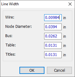
2.4.11. Colors
DipTrace allows the user to edit design area color template as well as all elements and print colors. Go to "View \ Colors" from the main menu.
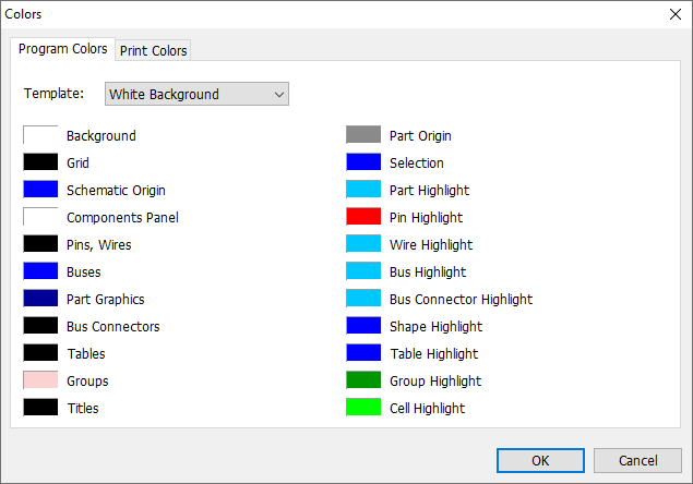
Three color templates are available: White Background, Black Background and User Defined. White background is a default template. Black background is more eye-friendly and very popular with engineers. To select color template, use the Template drop-down list.
To define color of specific element, left-click on the corresponding color rectangle, and select a new color in the pop-up dialog box. Standard templates doesn't allow for user customizations, therefore User Defined template is activated automatically.
Select the Print Colors tab to adjust colors when printing the schematic.
Schematic module and Component Editor share same color template. This means that if you need to change colors in the Component Editor, you have to change them in the Schematic. The same rule applies to PCB Layout and Pattern Editor.
2.4.12. Graphics mode
DipTrace Schematics and PCB Layout programs work in Direct3D, OpenGL and Windows GDI modes. You can select the graphics mode from the main menu "View \ Graphics Mode".
1. Direct3D is the fastest mode for regular Windows PC without high-end OpenGL hardware. This mode depends on hardware/drivers/versions, some machines still experience problems due to outdated OS/drivers.
2. OpenGL is a bit slower than Direct3D, but less dependent on hardware/drivers. OpenGL mode is the best choice for high-end engineering stations with professional OpenGL graphic adapters.
Try which one works better for you.
3. Windows GDI is an alternate mode if both Direct3D and OpenGL modes do not work correctly with your machine. It is much slower, but less dependent on drivers/hardware/OS. This mode is enough for comfortable work on small and medium projects.
2.4.13. Units
It is possible to work with the following measurement units: millimeters, mils and inches.
To change the current units, select "View/ Units" from the main menu or use Shift + U default keyboard shortcut.
2.4.14. Precision
Precision
DipTrace allows adjusting the precision rate for project values and the grid.
Select View/ Precision… to open the following dialogue-box:
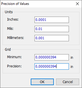
Configure the precision level by defining the number of decimal places (up to ten) for all the values used in the project by units.
You can also set the minimum grid size and grid precision for the current units. Those values are converted, when measurement units are changed.
Please note that high precision rates are used only at designing stage. When the project is saved into a file, precision up to 0.001 mil is applied.
2.4.15. Origin
Design origin is customizable, you can change its position at any time while creating or editing the schematic.
To display the origin, select "View \ Display Origin" from the main menu or press F1 hotkey (by default).
Origin can be defined with the mouse pointer or by coordinates (incrementally from current point). To define origin with the mouse, select "View \ Define Origin \ By Mouse Pointer" from the main menu or press button on the Elements toolbar, then define a new center point on the design area with a left-click (the design origin can be aligned with key points of some objects). To change origin by coordinates, select "View \ Define Origin \ By Coordinates" from the main menu.
To return origin to default position (center of the sheet), select "View \ Define Origin \ Default Position" from the main menu.
2.4.16. Grid
The user can create and edit objects on the design area freely or by the grid. If the grid is visible and Snap to Grid option is enabled, the components align by the first pin, while wires, buses, ports and shapes align by their key points.
To show/hide the grid, select "View \ Grid" from the main menu or press F11 default hotkey.
Select "View \ Snap to Grid" from the main menu, or press Alt+F11 hotkey (by default) to activate/deactivate snap to grid, when the grid is on.
If Snap to Grid option is disabled, the objects of the schematic are no longer snapped to the grid, but you can leave the grid visible.
When Snap to Grid option is disabled for the entire project, you can choose to snap to grid individual elements of your schematic (symbol, shape, text, image, etc.) by selecting Snap to Grid item from the right-click submenu of those elements, when the grid is on.
To open the grid size submenu, select "View \ Grid Size" from the main menu. Here you can select the grid size from the list or specify a custom size.
You can select it from the drop-down list on the Standard toolbar or with Ctrl + Plus sign (+), Ctrl + Minus sign (-) hotkeys.
Select "View \ Customize Grid" from the main menu to change the list of available grid steps.
2.5. Objects
2.5.1. Component
2.5.1.1. Review
Regular component in DipTrace includes one or several schematic symbols (parts) and attached pattern (possibly with a 3D model). Schematic symbol consists of pins, shapes and text (marking) elements.
Change pin type and other pin properties in the Pin Properties dialog box. To start/finish inversion in the pin name use the Tilde Sign (~) hotkey.
In the Schematic it is possible to place component parts from the Place Component panel or from the Place Component dialog box.
For multi-part components, you can select part or a group of similar parts. Assign RefDes, Value, Name, Part, Manufacturer, Datasheet or Additional fields as part markings of the component on the design area. When component is on the design area, the user can move, rotate, flip, replace, update or change current schematic sheet for the component, etc.
2.5.1.2. Multi-part components
DipTrace allows the designer to create and use multi-part components in the program. Components of this kind have special reference designators consisting of component RefDes and part RefDes after the point (for example parts of "D1" component are marked "D1.1", "D1.2", etc). Certain parameters of multi-part components can be changed directly in the Component Properties dialog box in the DipTrace Schematic, for example, RefDes and the name of exact part.
When multi-part component is selected in the component list on the Place Component panel, press All Parts button, and select current part which you want to place.
The number of parts is displayed in the upper-right corner of the symbol's preview. It is also possible to select part in the Place Component dialog box.
Multi-part component may include similar or different parts. If "View \ Group Similar Parts" item is checked, similar parts are shown by a single item in the parts list and current part for placement is selected automatically.
Notice that Group Similar Parts works only for similar parts, not for multi-part components with different parts (even if they are visually identical).
The parts of a multi-part component are generally interchangeable. In DipTrace you can easily substitute one with the other - right-click on a part, select Swap Parts and choose the part for which you want to substitute the selected one. This option works with both types of identical parts of a multi-part component.
2.5.1.3. Net port
Net Ports are components that do not have attached patterns. These components exist only as a means of connecting pins without wires and do not have physical packages. You can create new net ports in the Component Editor or find them in the standard DipTrace libraries, select Net Ports library from the Components library group. This library hosts all the most popular net ports (incl. GND, PWR).
Place two or more net ports with the same name on one or several schematic sheets and connect wires to their pins to create a single net connected with net ports.
Notice that nets connected to the net ports are not automatically renamed to match the name of the net port.
You can use net ports with several pins to connect several wires at a time. Wires connected to the corresponding pins of connected net ports will be connected automatically. If pin numbers are different, the wires will not connect.
Reconnecting is possible simply by changing the net port name (right-click on the net port and select the first item from the submenu). However, we do not recommend renaming pins. Net ports can be used in hierarchical schematics (DipTrace will create global nets automatically).
A wire can show the direction of the signal for convenience. Right-click on a wire, and select Direction Arrows from the submenu, then select either Forward or Backward.
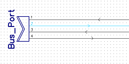
To remove the arrow, right-click on the wire, and select Direction Arrows from the submenu, then select None.
2.5.1.4. Place component
Place components directly from the Place Component panel or with Place Component dialog box. Select "Objects \ Place Component" from the main menu or press  button on the Objects toolbar.
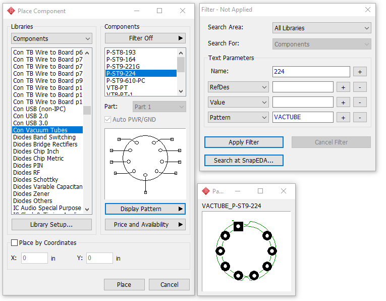
Select library group in the drop-down list, select library, and select component. Press Place button. Use Filter ON/OFF button to adjust filters or turn them ON/OFF. Press Library Setup to edit library groups, press Display Pattern to preview component pattern.
Press Price and Availability button to consult price and availability of the selected component from a featured supplier or all the suppliers from Octopart catalog.
Use R or Space bar to rotate component before placement. You can drag and drop the component to change its location; guidelines will appear while moving it to help you align it with other components.
2.5.1.5. Attached pattern
DipTrace allows the user to change attached pattern and pin numbers for existing component/s or attach new pattern/s directly in the Schematic.
To change attached pattern, right-click on the component, and select Attached Pattern from the submenu or press Attached Pattern button in the Component Properties dialog box.
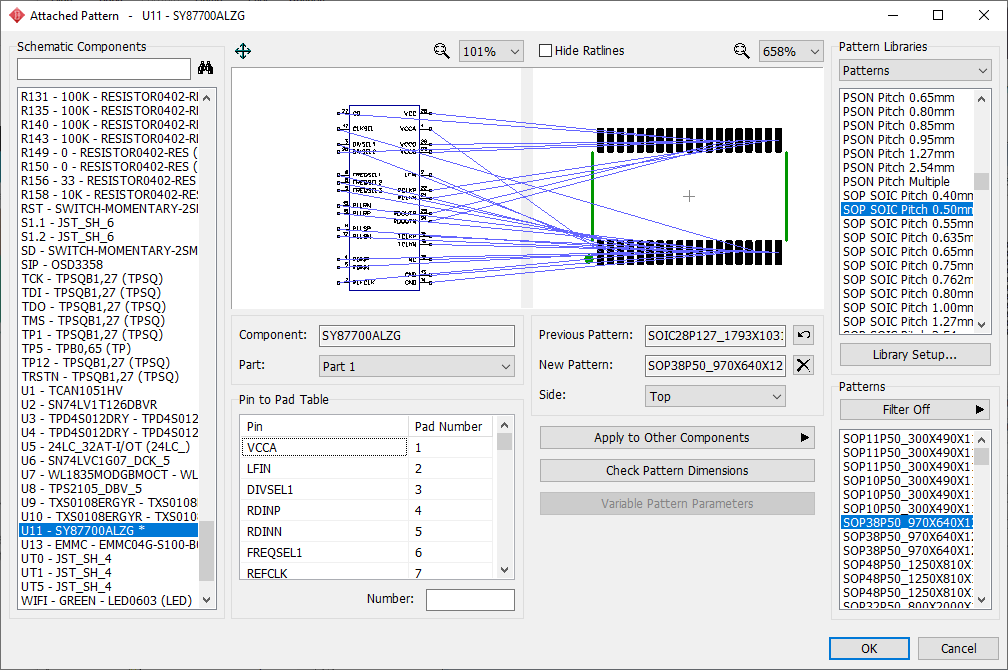
Select component from the list on the left side, then choose the library group from the Pattern Libraries drop-down list, select library, and select appropriate pattern from the list below (you can apply filters to find the pattern). Assign Pin to Pad connections in the corresponding table or visually in the component and pattern previews. Note that pads with the same numbers are automatically connected to one net. Use @ sign after the identical pad numbers to avoid errors.
You can also create connections between pads manually: left-click on a pad and then click on another one, with which you want to create a connection - a menu will pop up; confirm or cancel pad connection by selecting the respective option.
Press Apply to Other Components to apply selected pattern to similar components with the same name regardless of the pattern, or to components with the same pattern regardless of their name.
Designer can Undo to the previous pattern.
The Side drop-down list is good for SMD patterns with pads on both sides of the board (for example, EDGE connectors).
If it is a multi-part component, each part can be selected separately in order to define pin numbers, use the Part drop-down list under the schematic symbol preview field.
Attach Pattern dialog box is the same as in the Component Editor, but instead of all components of active library you see all components of current schematic.
2.5.1.6. SPICE Model
To define/change SPICE settings of a component, right-click it and select SPICE Model from the submenu. The following dialog box will pop up:
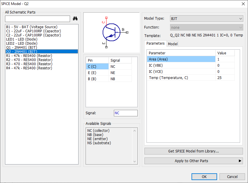
All the parts of the current schematic are displayed on the left. Left-click to select the required component from the list or use the search field to find it.
Pin-to-signal connections can be established using the table in the central part of the dialog box. The list of available signals with comments is located right below.
The dialog allows selecting the model type, defining parameters, model and signals for the components. Resistor, Capacitor, Inductor, Sources, Mutual Inductance and Transmission Line types do not require models and you can define their parameters manually. SubSkt type is often used to define logics, chips, etc., however, it can be used for almost any purpose.
Notice that models can be loaded from external ASCII files (usually available at manufacturers' websites or other locations on the Internet), just select the Model tab and press Load.
A SPICE model can also be loaded from the existing DipTrace library (press Get SPICE Model from Library button and select the respective Library group, Library and Component).
Once defined, component SPICE settings can be applied to Similar parts of the Component or All Similar Parts of the Schematic - press Apply to Other Parts button and select the required option.
Template line shows how the component will be displayed in the Spice netlist. Notice that you can scroll it to the right if necessary, because templates may be quite long.
If you are not familiar with SPICE language, we recommend using SPICE Language Documentation available on the Internet to discover more details.
After defining SPICE models for the schematic components you can run a built-in NGSPICE Simulator.
2.5.1.7. Properties
Right-click on a component, and select Properties from the submenu to open the Component Properties dialog box.
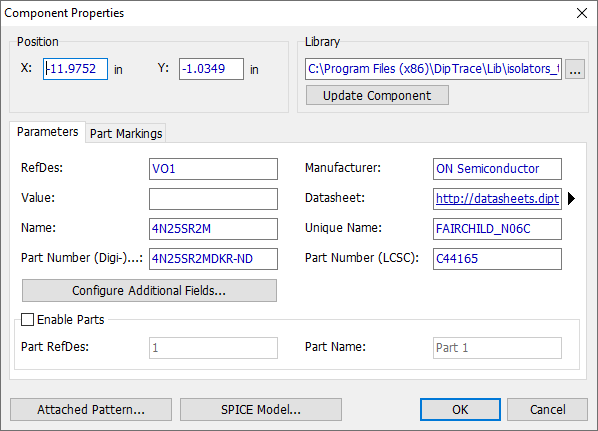
Here you can adjust component position by setting X and Y coordinates.
Component can be updated from the selected library. Press  button to browse for the required library file. Press Update Component button to apply changes.
A typical component has the following parameters: RefDes, Value, Name, Manufacturer, Datasheet, Additional fields, Part RefDes and Part Name (for multi-part components). RefDes is a unique component identifier.
Press Configure Additional Fields button to add more descriptive fields.
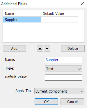
New fields can be added to the Current Component, Selected Components, Similar Name Components, components with Similar Set of Fields or All Components.
Enable Parts checkbox allows the designer to change internal RefDes and name of each part of multi-part component.
In the Markings Tab of the Component Properties dialog, you can choose to show/hide certain marking/-s (RefDes, Value, Name, etc.) or apply Common (default) settings to a given component. If you are dealing with a multi-part component, you can also select whether to show/hide or apply common settings to the markings of individual parts.
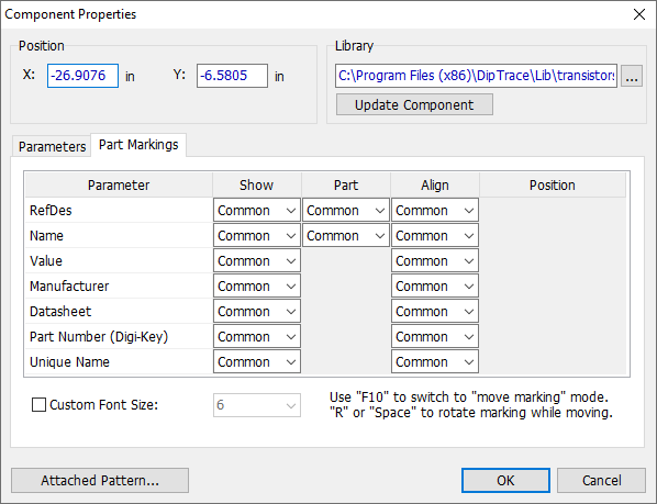
To define marking alignment settings, select the necessary option from the drop-down in Align column. The markings can be adjusted by the top, bottom, left, right, the center or corner of the component. You can also apply Common or Auto settings. In the first case, the software will use default parameters set for the entire project (View/ Part Markings). If Auto mode is selected, DipTrace will automatically select the best location for the markings. There is one more Aligning option - Position. Use it for precise Markings placement. Once selected, an active line appears in Position column. Press button to select the location of Markings anchor point, set its coordinates and rotation angle.
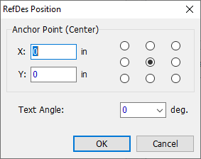
To change shift and spacing for the component text markings, select "View/ Move Part Texts" from the main menu or press F10 hotkey (by default). To rotate component markings while moving, press R or Space hotkeys.
2.5.1.8. Signal delay
Bond wires inside electronic component's package connect pads to the die. These wires introduce a signal delay, which should be accounted for in high-speed designs. Manufacturers report this in-device pad signal delay in picosecond time or as a length in the datasheets.
Pad signal delay value is considered for phase and length tuning and is added to the total length of the tracks when on the circuit board. We recommend setting up signal delays when designing a component in the DipTrace Component Editor, but you can also set it directly on the schematic (delay value is valid only for this schematic and PCB, this change does not affect the component in the library).
To set pad signal delay in the Schematic, right-click on the component and select Pad Signal Delay from the submenu or right-click on the pin and select Signal Delay.
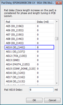
Select pad from the list (if not selected already), and enter a signal delay in mils right below. Press OK to apply changes.
You can also assign pad signal delays directly in the PCB Layout and Component Editor (recommended).
2.5.1.9. RefDes renumbering
Reference designators can be renumbered from the top-left to the bottom-right corner of the schematic sheet by rows or columns for convenience of exploring the schematic. Select "Tools \ RefDes Renumbering" from the main menu or right-click on any component, and select RefDes Renumbering from the submenu:
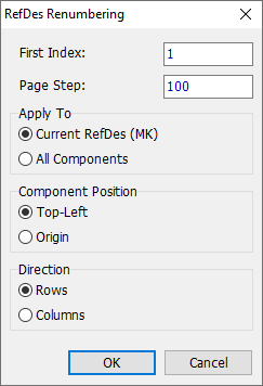
Renumbering can be applied to all reference designators of schematic or only to current RefDes (option is available only if you called RefDes Renumbering dialog box from the component submenu). Component position in the renumbering array can be determined by its top-left corner or by its origin.
Page Step value means page start increment index in the RefDes naming procedure (i.e. if the Page Step is 100, reference designators on the second page will be R101, R102, IC101, etc.).
Renumbering is possible by rows and by columns:
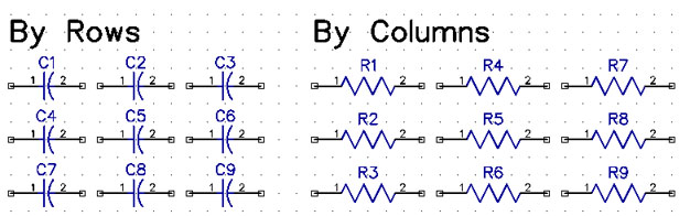
2.5.1.10. Pin properties
DipTrace Schematic allows the designer to change pin properties. Right-click on the pin, and select Pin Properties from the submenu. The following dialog box will appear:
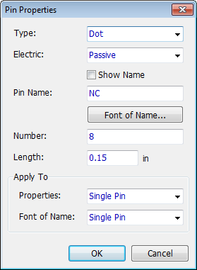
Here you can change the graphical pin type, electric type for ERC verification, pin name, and pin number. Pin number is usually a pad number of related pattern.
There are 15 types of pins:
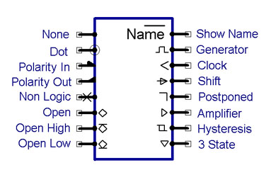
Press Font of Name button to adjust pin name font size, line and text width.
To start/finish inversion in the pin name use the Tilde Sign (~).
Properties and font of pin names can be applied to: single pin, selected parts and to all parts of current schematic.
2.5.1.11. Assign Supplier
In DipTrace you can consult prices and availability of the components used in your design in Octopart’s supplier database. The best supplier can be assigned to each component. This information can subsequently be included into the bill of materials.
To select suppliers, go to Tools/ Assign Suppliers. The following dialog will pop-up:
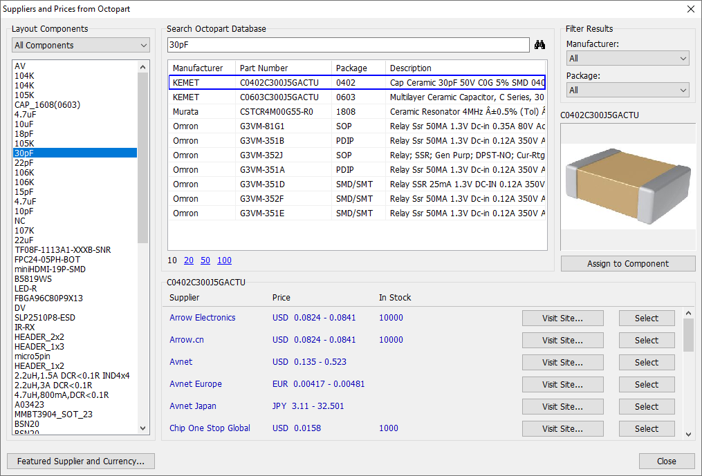
To assign a supplier to a component:
1. Select a component in the Layout Components section on the left. Using the drop-down menu you can filter the list to display Assigned, Not Assigned or All Components.
2. Review the component specifications in the central part of the dialog and select the appropriate one. To filter the search results by Manufacturer or Package, use the respective drop-downs on the right. You can Search Octopart Database directly from DipTrace to look for specific parts or to narrow down the suggested options.
3.Consult prices and availability of the selected component from different suppliers. Note that Digi-Key is the featured supplier by default, meaning that it’s automatically selected as the provider. You can easily re-assign the supplier for a certain part by pressing the Select button. To change your preferred supplier and currency, press the Featured Supplier and Currency button.
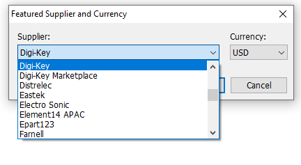
When done, press the Assign to Component button and proceed with the next component.
2.5.2. Net
2.5.2.1. Review
Nets in DipTrace Schematic consist of wires connecting component pins, buses, and ports for nets and buses. Net connections can be visual and logic (by name, without wires, with net ports). See Connecting for more information. All wire-to-bus connections are marked with net name or net number in the bus.
There are two modes of creating wires: automatic and manual (use M hotkey to switch between the modes while drawing the wire). Automatic mode draws the wire from the start point to the end point automatically, DipTrace avoids overlaying parts or wire segments with parts and wires of the same orientation if there is enough free space on the sheet. Manual mode allows the user to place wire segments step-by-step, use S or Space hotkeys to switch between the segments.
Nets can be renamed, wires can be hidden or moved to another sheet, net color can be changed, etc.
2.5.2.2. Net classes
Net classes organize nets and allow the user to automatically apply predefined parameters to newly created nets. To add/edit net classes or move nets from one net class to another, select "Objects \ Net Classes" from the main menu. The following dialog box will appear:
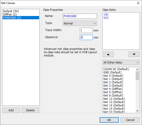
The user can add/delete net classes and edit their properties. Enter the name of the net class, select type (normal or differential pair) and enter values to set up the trace width, clearance, differential pair length and phase tolerances (if it is differential pair net class). These settings will be transferred to the PCB Layout, where more routing parameters will be available for customization.
DipTrace does not allow for nets outside any net class, hence all nets are automatically assigned to Default net class. The user can edit this class, but can not delete it.
Only blank net classes (no nets belong to the net class) can be deleted. Net should be moved to another net class before deleting. To move nets between the classes, use lists on the right side of the dialog box and Up and Down buttons.
Net classes can be loaded from the PCB Layout, select "Objects \ Load Classes" from the main menu and select the layout file to extract the net classes or use the Back Annotate feature ("File \ Back Annotate" from the main menu).
2.5.2.3. Placing wires
There are several ways to create wires in the Schematic:
1. Default (Visual). Place wire with the mouse in the default mode (or in the Place Wire mode), left-click on the start point of the future wire (pin or wire segment), and then left-click on the end point (pin, wire segment or bus).
The software draws wires and creates corners automatically – the wire never overlays any components or wire segments with the same orientation (depends on the free space on the sheet). Press M hotkey to place wire segments step-by-step and create corners manually (use S or Space hotkeys to switch between 0>90 and 90>0 segments, U hotkey removes the last placed segment).
Right-click, and select Enter from the submenu to finish/cancel wire placement, or use Enter or Esc hotkeys.
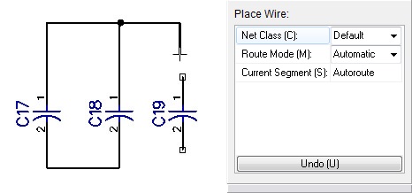
2. From the submenu. Right-click on the pin, and select Add to Net from the submenu, choose net in the drop-down list, and press OK. It is possible to connect pins to existing nets without wires, check Connect without Wire box in the Add to Net dialog box.
3. Connection Manager. To create wires with the Connection Manager, select "Objects \ Connection Manager" from the main menu or right-click on any net, and choose Connection Manager. It is possible to edit net list by adding/deleting pins to/from existing nets and to add new nets to the schematic.
See connecting for more details about using buses, net ports and connection without wires.
2.5.2.4. Editing wires
The user can move wires orthogonally. To enable wire editing mode, select "Objects \ Circuit \ Edit Mode" from the main menu or press button on the Objects toolbar. This mode is activated automatically, when you try to drag existing wire segment with the mouse.
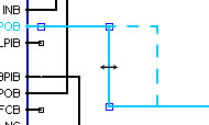
To add nodes to the wire segment, right-click it, and select Add Node from the submenu.
To change net for the wire connected to the bus, right-click on the wire, select Bus Connection from the submenu, and select a new net from the pop-up dialog box. To create a new net, enter its name in the Bus Connection dialog box, and press OK.
To delete wire segment, right-click it, and select Delete Line or Delete Wire from the submenu. The first option deletes a single straight line, the second – all segments of the wire between two connection points. Net structure can be changed.
The user can move a wire or entire net to another schematic sheet (if it is multi-sheet schematic). Select Change sheet from the right-click submenu.
Notice that you can not move wire to another sheet if it is connected to non-moving objects (components etc.). Therefore, if you want to move some wire to another sheet, select it together with connected components and move altogether to another sheet.
2.5.2.5. Connecting wires
DipTrace Schematic allows the user to connect pins with wires, net ports, buses and bus connectors, as well as connecting pins without wires.
1. Bus and Bus Connectors. To connect pins or wires with a bus, you should place a bus first, then connect wires or pins to the bus. The bus is a good choice when you need to connect many points in different parts of the schematic (in this case one bus replaces tens or even hundreds of wires with a single thick blue line). See Bus Review topic. Use bus connectors to connect buses on different schematic sheets (pages).
2. Connection without wire. To connect pin to any net without wire, right-click on the pin, select Add To Net from the submenu (item is visible if at least one net exists on the schematic), then select net from the drop-down list, and check Connect without Wires checkbox. Press OK. Please see the picture below: U2: Pin 4 (inverted MCLR) is connected without a wire.
3. Connect Nets by Name. To connect wires (nets) by name, right-click on any wire, and select the first item with the net name from the submenu. Now type in the name of existing net, which you want to connect with this wire, and press OK. The program may warn you that such net already exists and whether you want to connect wires by name (the warning message pops up only if Connect Nets By Name checkbox is unchecked for one or both nets).
Nets connected by name does not have any special marks, but when hovering over the wire with the mouse, you see two visually unconnected wires highlighted.
If you check Connect Related Wires Only checkbox in the Net Properties or Rename Net dialog box, DipTrace will connect only the wires which are visually connected. Therefore, you can easily move groups of wires between the nets by simply renaming them without deleting existing nets, which are logically connected with the wires being renamed. Two connected wires can not belong to different nets.
Notice that only global nets allow for connecting pins on different hierarchical levels.
4. Net Ports. Place two or more net ports with the same name on one or several schematic sheets and connect wires to their pins. Please see the picture below: U2: Pin 5 VSS is connected to the GND net with the net port.
Notice that nets connected to the net ports are not automatically renamed to match the name of the net port.
You can use net ports with several pins to connect several wires at a time. Wires connected to the corresponding pins of connected net ports will be connected automatically. If pin numbers are different, the wires will not connect.
Reconnecting is possible simply by changing the net port name (right-click on the net port and select the first item from the submenu). However, we do not recommend renaming pins. Net ports can be used in hierarchical schematics (DipTrace will create global nets automatically).
The picture below shows all aforementioned ways of connection:
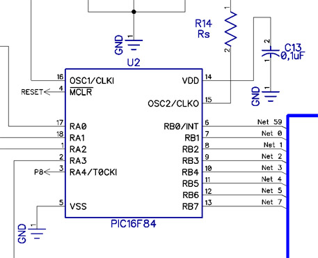
Here you can see "Net 59 – Net 7" connected to the bus, U2:VSS and C13:1 connected together via the GND net ports, U2:MCLR(inv.) and U2:RA4 connected to RESET and P8 nets without wires.
2.5.2.6. Properties
Right-click on the net, and select Properties from the submenu. The following dialog pops up:
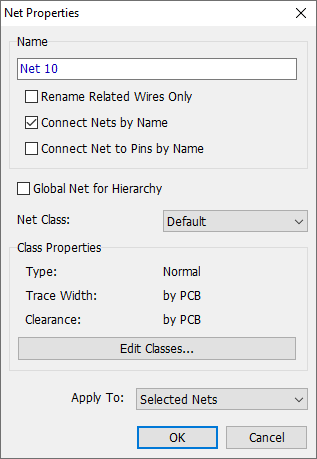
The Name section allows the user to rename entire net or rename only related wires (Rename Related Wires Only checkbox). If renaming only related wires, a group of visually connected wires will be disconnected from existing net and logically connected to a new net (by name). If you would like to connect wires by renaming them, enable Connect Nets by Name checkbox.
Connect Net to Pins by Name – connect all component pins with a net, if they have similar names.
Global Net for Hierarchy checkbox allows the designer to use a single net on different hierarchical sheets (different hierarchical levels). The net will not be separated by the blocks, i.e. all pins connected to the global net in hierarchy will be connected together in the layout, even if they are located in different hierarchy blocks. Global net is created automatically if some wire is connected to net port inside the hierarchical sheet.
Net Class – here you can change the net class of the net and preview its properties (type, trace width, clearance, etc.).
If Hide Power or Ground main menu item is enabled, the wire(s) will become hidden when you hide power objects.
2.5.2.7. Connection Manager
Connection Manager is another tool to work with net structure. It is very convenient, especially for complex schematics. Select "Objects/ Connection Manager" from the main menu or right-click on any net, and select Connection Manager from the submenu.
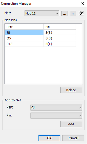
Here you can select net from the drop-down list. All pins of the net appear in the Net Pins table.
You can rename the net with the button or delete it with the  button. Press
  to add new net.
To delete pin from the net, select it in the table, and press Delete button.
To add new pin to the net, select component/part and a pin of this part, then press Add button.
2.5.3. Differential pair
2.5.3.1. Review
Differential pair signaling is a method of transmitting high-frequency low-voltage signals using two tightly coupled conductors (tracks on the circuit board). One track carries a signal and the other one carries an equal, but opposite image of the signal. Differential pairs are EMI immune, they generate less noise than single-track connections and, basically, are the only acceptable way to transmit high-frequency pulses on a circuit board.
DipTrace provides tools to create and edit differential pairs on the schematic and directly in the PCB Layout. Differential pair declaration can be put on the nets that already exist on the design area. Create a special type Differential Pair net class prior to defining a differential pair. Net classes manage all differential pair properties and routing constraints. Differential pairs are not allowed to have parameters outside a differential pair net class. DipTrace does not impose any restrictions on how many classes can be created.
The software controls various aspects of differential pair routing in the net class parameters (also available in the Schematic): trace width, gap, clearance to other objects, maximum total uncoupled length for two tracks of the pair, tolerance for length difference, dynamic phase tolerance, and phase error length for a differential pair net class.
Diff pair parameters are verified as DRC constraints in the PCB Layout.
2.5.3.2. Create differential pair
In order to create a differential pair in DipTrace, proceed to the Net Classes dialog box ("Objects \ Net Classes" from the main menu) and create a new net class. Press Add button, and select Differential Pair Type.
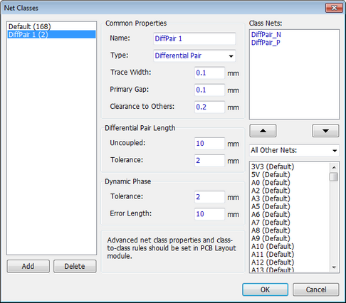
Class properties allow the user to change trace width, primary gap between the traces, clearances to other objects, differential pair length and dynamic phase settings. These parameters will be automatically transferred to the PCB Layout. Press OK to close the Net Classes dialog.
Now go to "Objects \ High Speed \ Define Differential Pair" from the main menu. In the pop-up dialog change pair name, color, and define positive and negative nets of the pair with the corresponding drop-downs or by pin pointing nets directly on the design area (just press  or
or  buttons and click on the pad of the net to put a differential pair declaration).
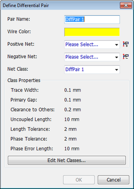
Notice that the previous net name will be disregarded in favor of the new one, typically it consists of a diff pair name + positive or negative net index.
Press Edit Net Classes button to open the Net Classes dialog box if you need to.
Select differential pair net class from the drop-down list, and apply changes by pressing OK button. Differential pair nets are marked with a special  symbol directly on the design area. Custom diff pair color also applies.
Notice that differential pair can not exist outside differential pair net class.
2.5.3.3. Edit differential pair
Editing differential pair wires does not differ from editing any regular nets and wires. However, with some special features available in the right-click submenu. If you are new to the software, please review Editing Regular Wires topic first.
When you hover over one of the differential pair nets with the mouse cursor, current wire and a differential pair symbol of the other wire are highlighted.
2.5.3.4. Diff pair properties
Right-click on any wire that belongs to a differential pair, and select Properties from the submenu.
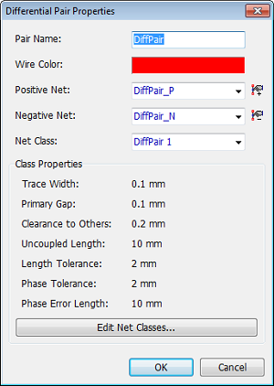
This dialog box allows the designer to change differential pair name, wire color, define other nets to the differential pair, change current net class, and review differential pair routing parameters. Net class defines all differential pair routing parameters. If you need to change them, you need to change current net class. Press Edit Net Classes to manage and edit Net Classes.
Notice that differential pair can not exist outside differential pair net class.
2.5.3.5. Differential Pair Manager
Differential Pair Manager is the most convenient way to create/edit/delete differential pairs in complex projects. Go to "Objects \ High Speed \ Differential Pair Manager" from the main menu. The following dialog box will pop up:
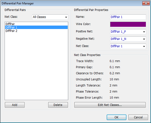
Sort differential pairs by net classes with the Net Class drop-down list.
Select differential pair from the list and review or change all differential pair parameters. Press Edit Net Classes to open the Net Classes dialog box for adding/deleting/editing net classes. In order to add or delete differential pair use Add or Delete buttons. Press OK to apply changes.
2.5.4. Bus
2.5.4.1. Review
Bus allows for visually grouping and compacting various nets (replacing tens or hundreds of wires with a single thick blue line). Buses also allow the designer to visually connect nets on different schematic sheets/pages. All wire-to-bus connections are marked with the net name or net number in the bus.
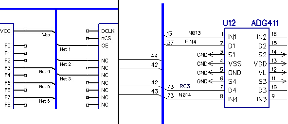
Each bus has its own list of bus nets. While connecting wire to the bus, you can connect it to the net which is already inside the bus or add new net. If you need to change nets in the bus, right-click on the wire segment connected to bus, and select Bus Connection from the submenu.
Bus connectors allows the designer to connect buses on the same or different schematic sheets. If two or more bus connectors have the same name, all buses connected to them will automatically merge into a single bus.
2.5.4.2. Placing a bus
To create a bus, select "Objects \ Circuit \ Place Bus" from the main menu or press button on the Objects toolbar and draw the bus line segment-by-segment. You can terminate bus on the other bus line, bus connector or on empty spot. To terminate or cancel bus placement, right-click while drawing the bus, and select corresponding item from the submenu, or use Enter and Esc hotkeys respectively.
S or Space hotkeys allow the user to switch between 0>90 and 90>0 segments. U hotkey undoes the last segment.
Bus lines connected to bus connectors with the same name are united automatically. Schematic bus structure can be changed by changing the names of bus connectors. Be careful while renaming bus connectors if their buses already have connected nets.
2.5.4.3. Editing a bus
You can move bus segments in the edit mode or default mode (in this case the edit mode is activated automatically). To activate the edit mode manually (for example, if you want to edit the bus, which lies under some component), select "Objects \ Circuit \ Edit Mode" from the main menu or press button on the Objects toolbar. Now left-click on the bus segment and drag it:
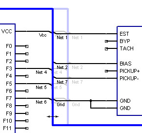
To add node to the bus segment, right-click it, and select Add Node from the submenu.
Single bus can be located on different schematic sheets (not hierarchy blocks).
To connect bus lines on different schematic sheets:
– Place bus connectors on both sheets,
– Define the same names to the bus connectors,
– Connect bus lines to the connectors.
You can move bus to another schematic sheet. In this case, the bus will disappear from the current sheet, but all wires will be still connected to this bus. Bus connectors and connected bus should be moved together, just like a regular net.
To delete bus segment, right-click it, and select Delete Line from the submenu. Select Delete Wire from the right-click submenu to delete the wire. Select Delete from the right-click submenu to delete entire bus.
2.5.4.4. Bus nets
To open the list of bus nets, right-click on the bus, and select Bus Nets from the submenu. The following dialog box will appear:
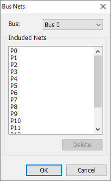
Here you can choose a bus and delete nets. After deleting, the structure may be changed, so please be careful.
2.5.5. Shape
2.5.5.1. Review
Shapes allow the designer to make any custom drawings directly on the schematic sheet.
The following shape types are available: Line, Arc, Rectangle, Filled Rectangle, Obround, Filled Obround, Polyline, Polygon, Text, and Picture.
2.5.5.2. Create
To place a shape, press button on the Objects toolbar and select the corresponding shape, or go to "Objects \ Place Shape" from the main menu. Then draw a shape on the design area.
To place a Line, press  button on the Objects Toolbar. Left-click to anchor the starting point and the end point. When drawing the line, it’s dimensions will be displayed by DipTrace.
To place an Arc, press  button on the Objects Toolbar. There are three modes for Arc placement in DipTrace. Left-click to anchor the starting point, then right-click to select placement mode:
| § | Start - Center - Angle - with this mode selected an arc with a certain angle is built based on a circle with defined radius. Anchor the starting point, the center point of a circle will appear; the radius of the circle is equal to the distance between the starting point and the center point. Move the center point away from the starting point to get a circle with desired parameters. Next left-click and adjust the angle of the arc. Left-click to anchor the end point of the arc. |
| § | Start - End - Radius - in this mode an arc of desired radius is built between the Start and End points. Place the Start and End Points and move the mouse pointer to adjust the radius of the arc. Left-click when done. |
| § | Start - End - Middle Point - in this mode an arc is built based on three points. Place Start and End point, the third point will appear on the line between them. Move the point to get an arc with desired parameters. |
Choose Clockwise or Counter-Clockwise from the right-click submenu to define the concavity direction of the curve.
Select Cancel from the right-click submenu to cancel the arc placement.
When drawing an arc, it’s key parameters (radius, deg.) will be displayed by DipTrace.
To place a Rectangle/ Filled Rectangle, press  or
or  button respectively on the Objects Toolbar. Left-click to anchor the starting point, draw the shape and left-click in the end point. When drawing the shape, it’s dimensions will be displayed by DipTrace.
To place a Obround/ Filled Obround shape, press  or
or  button respectively on the Objects Toolbar. Left-click to anchor the starting point, draw the shape and left-click in the end point. When drawing the shape, it’s dimensions will be displayed by DipTrace.
To place a Polyline/ Polygon, press  or
or  button respectively on the Objects Toolbar. Left-click to anchor the starting point, draw the shape, left-click to anchor points, right-click in the end point and select Enter form the submenu. When drawing the shape, it’s dimensions will be displayed by DipTrace.
To define shape color and line width before placement, select "Objects \ Drawing Properties" from the main menu. However, it is possible to change these properties for objects already on the design area via Properties submenu.
2.5.5.3. Edit
To change shape size, select a shape, and drag its key points with the left mouse button.
Right-click on the shape object and move it to another sheet, if necessary (Change Sheet item).
For precise shape editing, use the Shape Properties dialog box.
2.5.5.4. Properties
2.5.5.4.1. Line
Right-click on a line, and select Properties from the submenu to open Shape Properties dialog box:
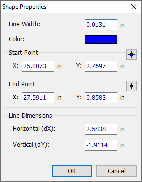
You can use pre-defined line width (Objects/ Drawing Properties/ Line Width) or set a new value for the given shape.
To change shape color, click on the colored rectangle and select a new one.
Start and End Points can be adjusted by changing X and Y coordinates or by using  button to set them by Mouse Pointer.
Finally, you can edit Line Dimensions, just type-in new values for Horizontal (dX) and Vertical (dY) tangent.
2.5.5.4.2. Arc
Right-click on an Arc, and select Properties from the submenu to open Shape Properties dialog box:
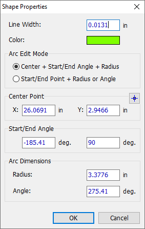
You can use pre-defined line width (Objects/ Drawing Properties/ Line Width) or set a new value for the given shape.
To change shape color, click on the colored rectangle and select a new one.
Select an Arc Edit mode: Center+Start/End Angle+Radius or Start/ End Point+Radius or angle. Type-in all the required values. Note that points can be defined by X and Y coordinates or set by Mouse Pointer upon pressing .
Finally, you can change arc Radius and Angle.
2.5.5.4.3. Rectangle/ Filled Rectangle
Right-click on a Rectangle/ Filled Rectangle, and select Properties from the submenu to open Shape Properties dialog box:
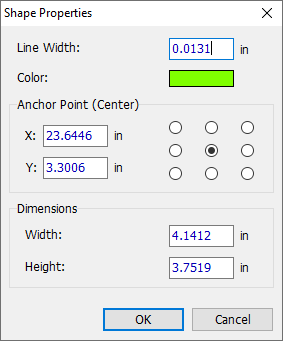
You can use pre-defined line width (Objects/ Drawing Properties/ Line Width) or set a new value for the Rectangle.
To change shape color, click on the colored rectangle and select a new one.
Next, you can change the position of an anchor point and type-in its coordinates for precise shape positioning.
Finally, you can edit shape dimensions.
2.5.5.4.4. Obround/ Filled Obround
Right-click on an Obround/ Filled Obround shape, and select Properties from the submenu to open Shape Properties dialog box:
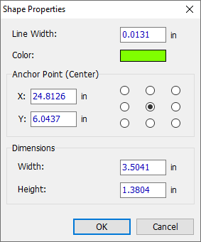
You can use pre-defined line width (Objects/ Drawing Properties/ Line Width) or set a new value for the Obround shape.
To change shape color, click on the colored rectangle and select a new one.
Next, you can change the position of an anchor point and type-in its coordinates for precise shape positioning.
Finally, you can edit shape dimensions.
2.5.5.4.5. Polyline/ Polygon
Right-click on a Polyline/ Polygon shape, and select Properties from the submenu to open Shape Properties dialog box:
|
|
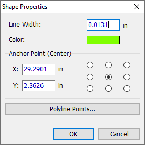
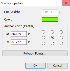
You can use pre-defined line width (Objects/ Drawing Properties/ Line Width) or set a new value for the Polyline shape.
To change shape color, click on the colored rectangle and select a new one.
Next, you can change the position of an anchor point and type-in its coordinates.
Finally, you can edit shape dimensions by clicking on Polyline Points/ Polygon Points button.
2.5.6. Text
2.5.6.1. Create
A multiline text can be placed in DipTrace. Go to Objects/ Place Text or press button on Objects toolbar.
Left-click on the design area and type the text.
Use Enter key to move to the next line.
Right-click on a free spot of the design area to return to default mode. You can drag and drop the text to change its location; guidelines will appear while moving the text to help you align it with other text objects.
To define text font type and size, width and color before placement, select Objects/ Drawing Properties from the main menu. However, it is possible to change these properties for objects already placed on the design area.
Note that tilde (~) before and after text is reserved by the software for placing a line over the pin name, which implies inversion; if you want a tilde symbol to appear as it is, you should place it twice:
~text~/~~text

2.5.6.2. Edit
To edit, double click on the text object or right-click on it and select Edit Text. The following dialog will appear:
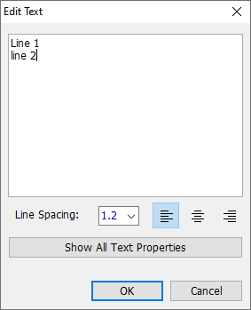
Here you can change the text, line spacing and alignment. Press Show All Text Properties button to access Text Properties dialog that allows for adjusting more text object parameters.
Right-click on a text object and select Font Type from the submenu. Vector and TrueType fonts are available. Vector font is recommended, if you use Latin characters. Unicode characters are supported only by the TrueType fonts.
To change text object size, select it and drag its key points with the left mouse button, the font size will change automatically.
Select Rotate from the text right-click submenu to rotate it at 90-degree step counter-clockwise. You can use R or Space hotkeys for the same purpose.
Right-click on the text object and move it to another sheet, if necessary (Change Sheet item).
2.5.6.3. Properties
To open Text Properties dialog, right-click on the text object and select Properties from the submenu.
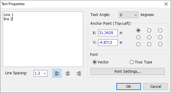
In the pop-up dialogue you can set line spacing and text alignment.
Choose an angle from the Text Angle drop-down or just type-in the required value to rotate the text.
The location of the Anchor Point of the text box is set by ticking the respective circle. Anchor Point is displayed as a cross. You can also set the coordinates of the Anchor point for precise text positioning.
Select Font Type: Vector font is recommended, if you use Latin characters; unicode characters are supported only by the TrueType fonts.
Press Font Settings button to open Font dialog (it can also be accessed by selecting Font in the text right-click submenu):
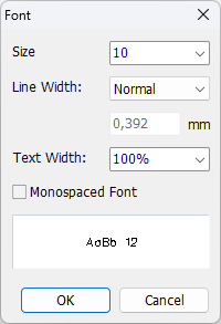
Here you can set the font size, select the Line Width from Thin, Normal, Bold or Customize it, and also define the Text Width and color.
Mark Monospaced Font to distribute character spacing evenly across the text, applicable to vector font only.
2.5.7. Table
2.5.7.1. Review
Table has a certain number of columns and rows.
Table field can contain any text aligned by left, center or right (Vector or TrueType fonts for Unicode characters).
To change column width or row height, use the Table Properties dialog box or select the corresponding item from the table submenu.
To change text and cell alignment, left-click on the table cell, and specify new text and alignment.
2.5.7.2. Create
To place a table, select "Objects \ Place Table" from the main menu or press button on the Objects toolbar. Then left-click on the design area, where the table should be created and you will see this dialog box:
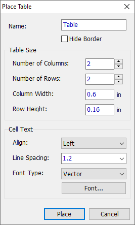
Specify a table name, number of columns and rows, column width and row height, alignment, line spacing and font type.
To define other parameters of the text placed in the table fields, press Font button. Click the Place button to create the table.
All table properties can be changed in the Table Properties dialog box.
2.5.7.3. Edit
To define text and alignment of the table field, left-click on the field and make all changes in the pop-up dialog box.
To change column width or row height, hover over the cell which belongs to the column or the row of the table, right-click to open the submenu, then select Column Width or Row Height, enter new values, and press OK. To change size of all columns and rows of the table, use the Table Properties dialog box.
To add columns and rows to the table, move the mouse cursor to the table border, right-click it and select the corresponding item from the submenu.
To insert columns or rows to the table, move the mouse cursor to the table field, right-click it and select the corresponding item from the submenu. Empty columns or rows will be inserted before selected cell.
To delete columns or rows from the table, move the mouse cursor to the cell, which belongs to the column or row, right-click it, and select Delete Column or Delete Row from the submenu.
To move table to another sheet, right-click it or right-click on any table field, and select Change Sheet from the submenu.
2.5.7.4. Properties
To change table properties, right-click on a table, and select Properties from the submenu. The following dialog box pops up:
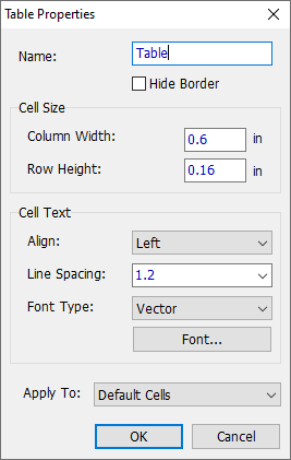
Here you can change the table name, column width, row height, alignment, and font by default.
Changes can be applied to:
– all table cells;
– cells with default settings;
– as default settings for new cells (not for existing cells).
2.5.7.5. Saving to file
Schematic table can be saved into Excel CSV file or into formatted text files.
To save table to a file, right-click on a table, and select Save to File from the submenu and decide on the file format (Excel CSV or Text File). CSV file is perfectly supported by popular spreadsheet programs (MS Excel, OpenOffice, etc.). When exporting to CSV file, DipTrace will ask you to set a Column Divider and decide whether to use Quotation Marks for values or not.
2.5.8. Bus connector
Bus Connectors allows the designer to connect buses on different parts of the schematic (including different schematic sheets).
All buses connected to the bus connectors which have the same name, are united into a single bus automatically.
Correctly connected bus connector has a green connection point. Blue connection point means that the bus line and the bus connector are not connected, even if visually everything is OK.
Notice that boxes around the names of the bus ports show that these bus ports are connected. Underlined means unconnected.
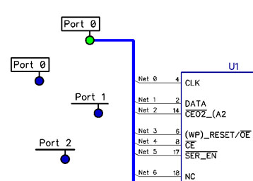
To connect bus lines on different schematic sheets:
– Place bus connectors on both sheets,
– Define the same names to the bus connectors,
– Connect bus lines to the connectors.
Net ports basically serve the same purpose as bus connectors, but net ports only connect one or several nets. See Connecting for details. User can easily change current sheet for selected bus connector, like for any other object. If bus connector is connected to a bus, select both and move them to another sheet.
2.5.9. Hierarchy
DipTrace supports hierarchical schematics based on the multi-sheet structure. This structure allows for vast block routing capabilities. There are two basic objects that are used in the hierarchy: hierarchy connectors and hierarchy blocks.
To create a hierarchical schematic, you should add new sheet to the schematic ("Edit \ Add Sheet" from the main menu), then go to "Edit \ Sheet Type \ Hierarchy Block" from the main menu to change sheet type. You can change sheet type for the second and all further sheets. The first sheet is always on top level of hierarchy, it is a main circuit, you can not delete it.
The next step is adding hierarchical connectors to the sheet. They are associated with block pins (IN/OUT). Select "Objects \ Hierarchy \ Place Connector" from the main menu or press  button on the Objects toolbar, then place connectors on the design area. The location of hierarchy connectors defines the location of the block pins on the main sheet.
Now design the subcircuit and connect its inputs and outputs to hierarchical connectors inside the block. You can use global nets to connect pins on different hierarchy levels. Net is always global if it is connected to net ports inside a hierarchical block (Net 15, connected to the GND pin on the picture below).
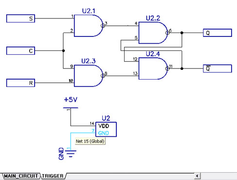
To place hierarchical block into the upper-level hierarchical block or to the main sheet, select "Objects \ Hierarchy \ Place Block" from the main menu or press  on the Objects toolbar. Select hierarchical sheet from the list and place it on the design area. You can place unlimited number of blocks. If there are several hierarchy blocks with the same content – the software will assign special indexes to reference designators and net names: <RefDes>_<Block Number> or <Net Name>_<Block Number>.
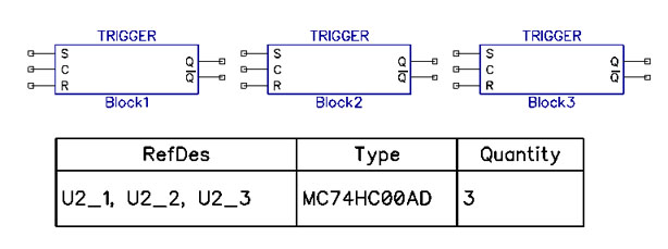
Notice that DipTrace supports multi-level hierarchy, but you should be very careful while designing schematic with hierarchy, because probability of making an error sufficiently increases.
2.5.10. Search objects
To find component or net on the schematic, select "Edit \ Find in Schematic" from the main menu or press Ctrl+F hotkeys (by default).
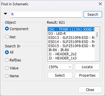
In the pop-up dialog box, select the object type (Component or Net) and the search criterion (All, RefDes, Value or Name). Then enter the full or partial search term and press Enter or click Search.
In the Results list, double-click an object or click Locate to highlight and center it in the design area.
To select objects, choose one or more entries in the Result list and click Select.
For direct editing, click Properties to open the object’s Properties dialog.
The Search dialog does not need to be closed while working with the schematic. It can be minimized by clicking the arrow in the upper-left corner.
2.6. Edit functions
2.6.1. Select objects
DipTrace has several ways to select objects or edit existing selection:
1. The mouse. Click on the object with a mouse button. Use left mouse button to select an object, and right mouse button – to open object's submenu. Notice that you can select overlaying objects by clicking the same button again and again, depending on the number of overlaying objects.
2. Default mode. In the Default mode hold down the left mouse button on empty area, and move the mouse pointer to draw the selection box. All objects surrounded by this box will be selected when you release the mouse button.
Use Ctrl or Shift hotkeys to add objects to the selection.
If you try to select one object from a group, the entire group will be selected.
To select all objects of the design, go to "Edit \ Select All" from the main menu or press Ctrl+A hotkeys.
3. Edit Selection. Go to "Edit \ Edit Selection" from the main menu. Edit Selection dialog box allows the user to select objects by type.
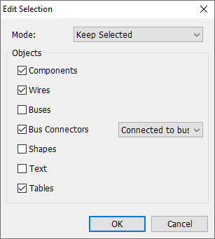
In the pop-up dialog box select the objects and one of the selection modes:
1. New Selection – deselect all previously selected objects and create a new selection based on your choice;
2. Add to Selection – add specified objects to existing selection;
3. Remove from Selection – remove specified objects from existing selection;
4. Keep Selected – deselect all selected objects, which do not correspond to the specified parameters. This mode allows the designer to select objects by type and area. Use box selection and Ctrl hotkey to define an area, then select Keep Selected mode which will deselect unspecified objects.
2.6.2. Cross Selection
DipTrace features Cross Selection and Cross Highlight between the Schematic and PCB, meaning that when objects (components, nets and pins) are selected or highlighted in the Schematic Capture, they are simultaneously selected/ highlighted in the PCB and vice versa.
To enable this feature, go to Edit/ Cross Selection in the main menu and mark Enable Cross Selection in the pop-up dialog.
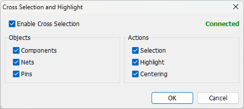
You can choose which objects will be selected or highlighted, and which actions will be synchronized between both modules when using this function.
To use this feature, make sure related schematic is assigned to the PCB (in the PCB Layout module got to File/ Layout Information from the main menu and in the Related Schematic section of the dialog press button to browse for and select the related schematic file).
2.6.3. General functions
There are following general editing functions: Delete, Cut, Copy and Paste.
Select objects before applying these functions.
To apply one of these functions to the objects, select a corresponding sub-item from the main menu ("Edit"). It is possible to use default hotkeys: Cut (Ctrl+X), Copy (Ctrl+C), Paste (Ctrl+V), and Delete (Del). Copying is also possible between the program instances.
To create the matrix based on selected objects, select "Edit \ Copy Matrix", define the number of columns and rows, spacings, and press OK.
2.6.4. Undo/Redo function
To cancel the last editing step and return to the previous state, select "Edit \ Undo" from the main menu or press the corresponding button on the Standard toolbar.
It is also possible to recover canceled steps. Choose "Edit \ Redo" from the main menu or press the corresponding button on the Standard toolbar. If you edit symbol after using the Undo tool, Redo tool becomes inactive.
You can select whether to consider Zoom a separate editing step or not, using Undo/ Redo Zoom item of Edit menu.
2.6.5. Undo/Redo Zoom
You can select whether to consider Zoom a separate editing step or not, by choosing from the following options:
Change if action not visible. If the editing step being canceled does not belong to the currently visible area of the design field, the first Undo command will return the view to the previous scale to make the location visible again; the second Undo command will cancel the action. If the location is visible on the design area, the first Undo command will cancel the action.
Change Always. The change of the scale is always considered as a separate editing step. Undo command returns the view to the previous scale.
Do Not Change. Undo command cancels the last editing without changing the scale.
2.6.6. Move/Rotate objects
To change location of some objects select them, and drag to a new location. If you move components, all wires connected to them will also change.
You can use the arrow keys to move selected objects. Hold down the Shift key for orthogonal moving.
To rotate object counter-clockwise, select it, and press R hotkey or select "Edit \ Rotate" from the main menu.
2.6.7. Align Objects
Select objects on the design area, then go to "Edit \ Align Objects" from the main menu, or right-click on one of the objects and select Align Objects from the submenu.
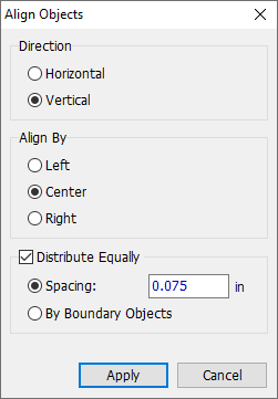
Select the alignment direction, then select how to align objects in the row or column (left, center or right) and set distribution settings by objects' boundaries or equally with a custom spacing.
You can group multiple objects into one so they will stay together if they are aligned or distributed.
At least two objects (or groups of objects) have to be selected for the Align tool to become available because the alignment is relative.
2.6.8. Group
Group is an abstract object which unites several design objects. Group defines some similar editing properties: fixed position relatively to each other, rotation according to the center of the group, all objects of the group will be selected when one of them is selected.
Borders and center point of a group are clearly marked. When any object of the group is highlighted – the group is highlighted.
To create a group, select objects, and go to "Edit \ Group" from the main menu. To ungroup objects, select any object of existing group, and go to "Edit \ Ungroup" from the main menu or use the right-click submenu. Visibility of menu items depends on the state of selection.
2.6.9. Lock/Unlock objects
To lock selected objects (prevent moving, editing, etc.) select objects first, then right-click on one of them, and choose Lock Selected from the submenu, "Edit \ Lock Selected" item from the main menu or press Ctrl+L default hotkeys. To unlock selected objects, go to "Edit \ Unlock Selected" from the main menu or Unlock Selected from the right-click submenu. Locked objects highlight in lower contrast when selected.
2.6.10. Working with sheets
Schematic may contain several sheets. To connect signals on different sheets, use bus connectors, net ports, connecting without wires, and connection by name. To add new sheet to schematic, select "Edit \ Add Sheet" from the main menu.
All sheets of the schematic are listed as tabs in the bottom-left corner of the design area:

To change current sheet, left-click it or right-click to open the sheet submenu. You can insert, delete, rename, move sheets left or right, and change sheet type. Hierarchy blocks are created based on the sheets, they are displayed together with regular sheets on this bar. To change sheet type, select "Edit \ Sheet Type" from the main menu (available for 2nd+ sheets), or right-click on the sheet tab, and select "Sheet Type \ Hierarchy" from the submenu. See Hierarchy for details.
You can move objects between schematic sheets, just right-click on an object, and select Change Sheet from the submenu.
A wire can show the direction of the signal for convenience. Right-click on a wire, and select Direction Arrows from the submenu, then select either Forward or Backward.
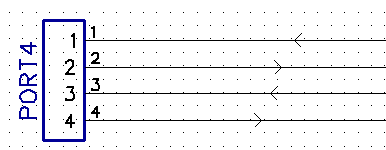
To remove the arrow, right-click on the wire, and select Direction Arrows from the submenu, then select None.
2.7. Verification
2.7.1. Electrical rule check
ERC feature allows the designer to check electrical rules for the schematic. To set up ERC, select "Verification \ Electrical Rule Setup" from main menu.
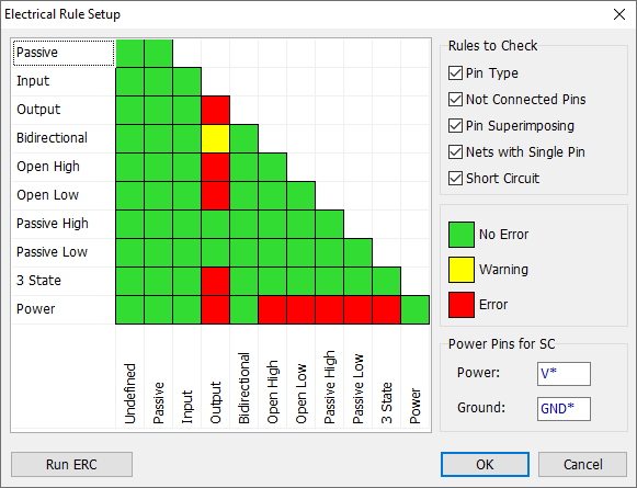
Check the Pin Type checkbox to verify the compatibility of connected pins according to the colored grid. Left-click in the corresponding grid cells (where the pin types cross) to set up errors and warnings. Errors are red, warnings – yellow, green means that pins of selected types are compatible.
Check Not Connected checkbox and DipTrace will consider all not connected pins as errors.
Check Pin Superimposing checkbox – DipTrace will consider all superimposed pins as errors.
Check Only One Pin in Net – DipTrace will consider all nets with only one pin as errors.
Short Circuit – DipTrace verifies if pins with Power and Ground type are somewhere connected together causing the short circuit. Power and Ground pins have the same electrical type, therefore ERC uses the pin name masks to recognize these pins (use Power Pins for SC section below to set up the nets).
Press Run ERC to launch verification, or go to "Verification \ Electrical Rule Check" from the main menu. The error list or "No Errors" message will pop up. To localize an error, double click it in the list of errors. Launch the ERC again after fixing the errors to ensure that schematic is correct.
2.7.2. Hierarchy check
Hierarchy should always have strict tree structure without "closed" loops. Hierarchy verification allows the user to find these loops and reports them as errors.
A typical closed loop situation: Block_1 includes Block_2 inside it, Block_2 includes Block_3, and Block_3 includes Block_1.
To run this verification select "Verification \ Check Hierarchy" from the main menu.
2.7.3. NGSPICE Simulator
DipTrace features a built-in mixed-level/mixed-signal electronic circuit simulator. To launch it, go to 'Tools/ SPICE Simulator' from the main menu.
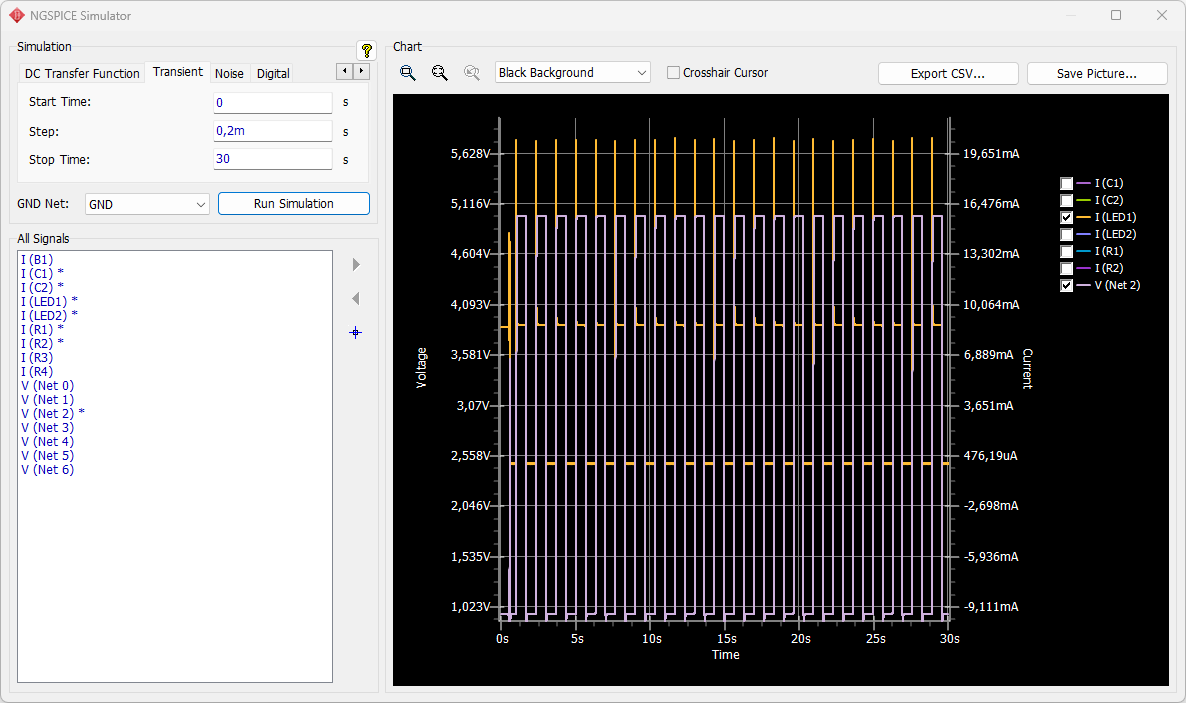
In the pop-up window you can select and set up the parameters for the Small-Signal AC, DC Transfer Function, Transient and Noise simulation - just select the respective tab and enter the required values. To check SPICE value Prefixes, press  button.
If you are designing a digital circuit, use Digital tab to run the simulation.
As soon as the simulation parameters are set, select ground net from the GND Net drop-down and press Run Simulation button.
Remember to define SPICE models for all the components of the circuit before running the simulation.
Double-click on the item in the All Signals list or use  and
and  buttons to add a signal to or remove it from the simulation chart. Press
  button to select a component or net directly on the schematic.
Right above the simulation Chart you can see a panel with a set of tools that facilitate its management:
 - select an area on the graph you want to zoom in; you can also use the mouse wheel to zoom the chart in and out;
 - return to the original zoom extents;
 - return to the previous scale.
You can also select Black or White background from the drop-down.
Mark the Crosshair Cursor check-box to change the shape of the cursor.
Press Export CSV to save a file with the simulation values.
To save the chart as an image in the PNG, JPEG or BMP format, press the Save Picture button.
Use check boxes next to the signals in the list on the right of the graph to display or hide the signal trace.
To highlight the trace that represents a signal, hover over the colored line next to it.
To change the color of the line that represents a signal, left-click on it in the list of signals and select a new color.
2.8. Plugins
DipTrace supports plugins, allowing the software's functionality to be extended and customized according to users' needs. This means that users can enhance their design process by adding specific features or automations that are not available in the default software.
Plugins can be created using any programming environment, offering flexibility to developers with different coding preferences and expertise. Whether you are proficient in C++, Python, or another programming language, you can develop plugins to integrate seamlessly with DipTrace.
To help users get started, DipTrace provides sample plugins along with their source codes. These examples serve as a valuable resource for learning how to develop and implement plugins.
In the Schematic Capture Convert Shapes to Dash/Dot Lines plugin is available. It allows users to convert selected shapes in their design into dashed or dot-dashed lines. It offers customization options for units, line types, and sizes of dashes and dots.
2.8.1. Convert selected shapes to Dash/ Dot
To convert a shape to a dash line, place and/ or select it in your schematic. To run the plugin go to Tools/ Plugins in the main menu and select Convert selected shapes to Dash/ Dot.
If you don't have .NET 8.0 installed, you will be prompted to install it.
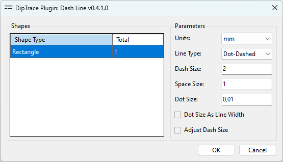
In the pop-up dialogue set the Parameters as required:
Units: mm, mil, inch
Line Type: Dashed or Dot-Dashed
Dash and Dot Size and the Space between the elements.
Mark Dot Size as Line Width to automatically adjust the dot size to match the Line width.
Mark Adjust Dash Size to allow the software to determine the dash size.
Click OK to apply the changes.
Click Cancel to discard changes.
2.9. Print, Sheet Setup
2.9.1. Print
Use the Preview dialog box before printing the schematic (we recommend printing directly from the Preview dialog box).
To print design without previewing it (which we do not recommend), select "File \ Print" from the main menu or press  button on the Standard toolbar. Schematic on the paper is what you actually see on the design area. It is also possible to show the page borders and titles on the design area.
To change title properties, use Titles and Sheet Setup dialog box.
You can use title templates or create your own title blocks with the Title Block Editor.
2.9.2. Preview
To open the Preview dialog box select "File \ Preview" from the main menu or press  button on the Standard toolbar.
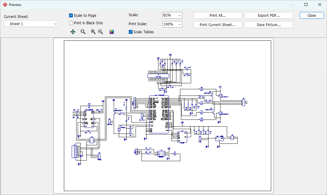
Schematic sheet is automatically scaled to fit the preview area. To change the scale of the sheet from 10% to 600%, use the Scale drop-down list.
Drag and drop to move sheet around a preview area.
Use  button to move schematic inside the sheet and the Print Scale drop-down list to change the circuit's size relatively to the sheet. Zoom In and Zoom Out easily.
Scale to Page checkbox scales the schematic and the sheet titles to fit the page.
If the Scale Tables item is checked, all tables on the schematic will be scaled when Print Scale value changes.
Press the Print All button to print all sheets and the Print Current Sheet button to print only the current sheet. Use Current Sheet drop-down list to change the current schematic sheet.
You can save your schematic as a PDF file or an image by pressing Export PDF or Save Picture buttons correspondingly.
To use custom colors for printing, press  button.
2.9.3. Titles and sheet setup
To set up the sheet size, edges, titles and create custom title blocks, select "File \ Titles and Sheet Setup" from the main menu or press  button on the Standard toolbar.
|
|
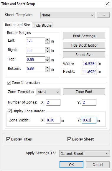
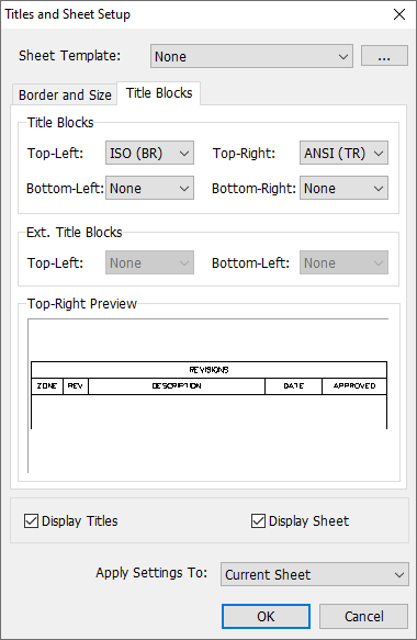
In this dialog box you can set sheet size, border margins, zones and title blocks.
The user can place up to four title blocks inside the sheet border (at four corners of the sheet) and two title blocks outside the sheet border (in the top-left and bottom-left corners). Zones are marked with numbers on top and bottom sides and with characters on left and right sides. It is possible to set two-zone marking templates: ANSI or ISO with Sheet Template drop-down list. Save titles and sheet sizes as the sheet template, just press .
Check Display Zone Border checkbox to show the outside zone border. Set zone width by X and Y axes.
Use the Title Block Editor to create your own or edit existing title blocks. Press Title Block Editor button to launch the editor.
To change print settings and select printer, press Print Settings button.
Sheet size and orientation depend on the printer settings. To change sheet parameters manually, press Sheet Size button.
It is possible to apply changes only to current sheet or to all sheets of the schematic.
2.9.4. Title block editor
To open the Title Block Editor, select "File/ Title and Sheet Setup" from the main menu and then press the Title Block Editor button in the pop-up dialog box.
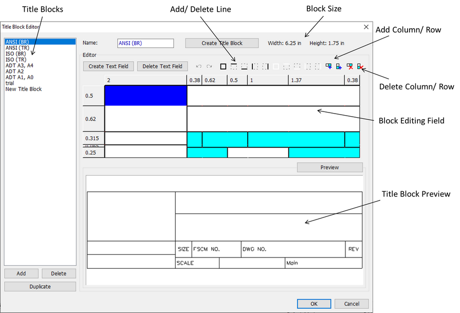
To create a new title block, press Add button or press Duplicate to get a copy of selected title block template. Then select a title block template from the list, and press Create Title Block button. In the pop-up dialog box enter the width and height of the title block, number of columns/rows, and press OK.
DipTrace will create a new block with columns and rows of equal size, depending on the total width/height of the block. Width and height of each column/row can be changed in the block editing field, just drag and drop size field borders (cells on the top and left sides of the Block editing field) or click them and enter exact values.
To create a text field, select one or several cells in the Block editing field, and press Create Text Field button. In the pop-up dialog box enter the text, select font, font parameters, alignment, and press OK or leave it blank to add text directly on the sheet. Field borders will be highlighted in red, they are invisible on the sheet. To draw or erase field border lines on the invisible cell borders, select required cell/s and press the corresponding button to add or delete the border lines.
Cells without a field are shown with gray color, regular fields (blank text fields) – with white color, fields with predefined text – aqua color, selected cells – dark blue color.
Press OK to save a title block and close the dialog box. All changes and custom fields are saved automatically and can be reapplied to other projects.
Notice that if you've made changes in active title block, you need to select it again in the Title Blocks tab in order to update the titles on the design area.
3. PCB Layout
3.1. User interface
3.1.1. Main window
DipTrace PCB Layout main window includes the design area, main menu, toolbars, the Component Placement panel, Design Manager with layers/objects/properties panel, and the status bar at the bottom (hint area and cursor coordinates).
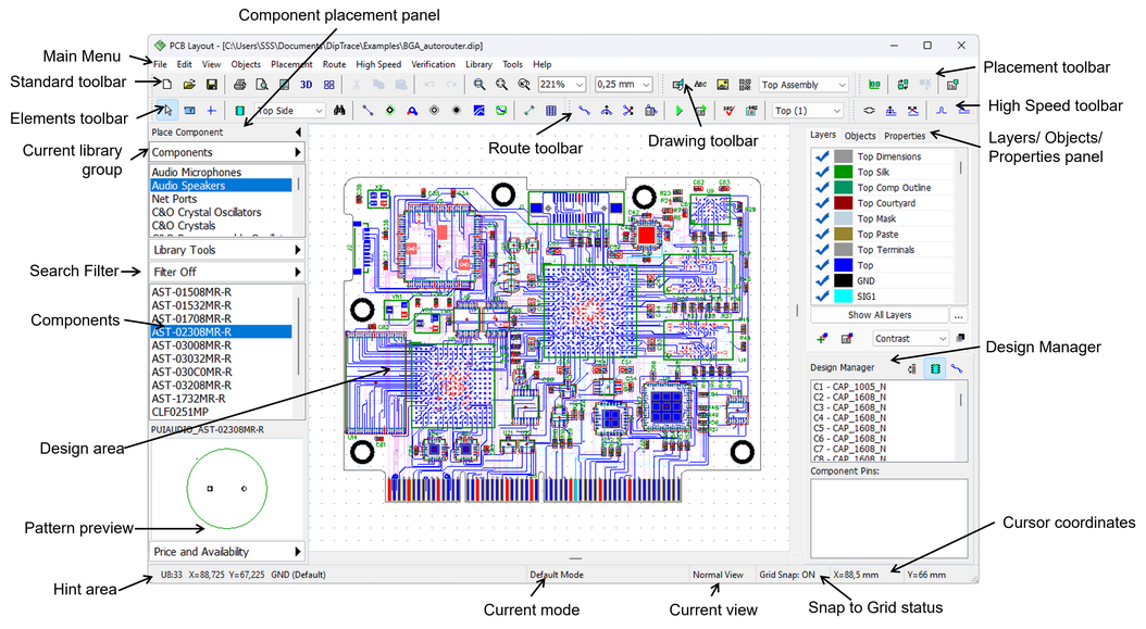
You can place and edit different objects (components, ratlines, traces, copper pours, shapes, tables, etc.) on the design area.
The main menu provides access to all common program features. Main menu: File, Edit, View, Objects, Placement, Route, High Speed, Verification, Library, Tools, Help.
Other interface elements:
Standard Toolbar – tools to work with files, cut/copy/paste objects, print, preview and configure titles, launch 3D Preview, change scale and grid size.
Elements Toolbar – tools to switch to the default mode, the ruler tool, change origin, apply search filters, select component placement side of the board, create ratlines, pads, vias, mounting holes, copper pours, board outline, dimensions, and tables.
Route Toolbar – tools to create and edit traces, run and set up the autorouters, check design rules, select current signal layer.
Drawing Toolbar – tools to draw shapes and polygons, place texts and images.
Placement Toolbar – arrange components and auto-placement tools.
High Speed Toolbar – define and edit differential pairs, add meanders, and phase tune tool.
Place Component (Library Manager) – work with libraries and components. Library groups, library tools, search filters, pattern preview. Search and place components on the design area.
Layers/Objects/Properties panel – (active tab depends on selected object/tool/mode).
Layers tab – work with layers (show/hide, add/delete/edit, change stack position and color) and change layer display mode;
Objects tab – show/hide different objects on the design area and block certain objects from being selected;
Properties tab – edit properties of selected tool/object.
Design Manager – navigates the user around the layout. Left-click in the list of components or nets to highlights object on the design area, double click to pan to selected component/net.
Status Bar shows (left to right) the current hint, mode, view, snap to grid status and cursor coordinates.
3.1.2. Toolbars
DipTrace PCB Layout has six toolbars, the Place Component panel, and Design Manager:
Standard toolbar

New – create a new layout. If current project has unsaved changes, DipTrace will offer to save it. PCB Layout can open one project at a time. If you would like to open several layouts, for example, to copy objects between them, just run several instances of DipTrace PCB Layout.
Open – open existing layout (*.dip) or schematic (*.dch) file.
Save – save current layout. If current project has unsaved changes, DipTrace will offer to save it. The program saves changes into the previously selected file. This tool is active only if there is unsaved activity.
Print – print the current layout. We recommend printing from the Preview panel. Sheet settings and titles are set in the Titles and Sheet Setup dialog box.
Preview – print preview dialog box.
Titles and Sheet Setup – open Titles and Sheet Setup dialog box to select sheet size and orientation, border margins, titles, zones, open the Title Block Editor, etc.
3D Preview – preview the circuit board in three dimensions (3D component models for patterns should be downloaded and connected to the patterns). Configure the folders with 3D models using the "Tools \ 3D Preview \ Patterns and Models Search..." main menu item.
Panelizing – open Panelizing dialog box to configure panelization of the current layout with V-scoring or Tab Routing options.
Cut – move selected object/s to the clipboard.
Copy – copy selected object/s.
Paste – paste object/s from the clipboard.
Undo – one editing step backward.
Redo – one editing step forward. This tool is active only after using the Undo tool. If you edit a layout after using the Undo tool, the Redo tool becomes inactive.
Zoom Window – set current scale and pan layout to defined area.
Zoom Extents – set current scale and pan layout to show all objects.
Undo Zoom – return to the previous scale and panning.
Scale – define the layout scale (from 25% to 800% or type in a new value). Changing the scale is possible with the mouse wheel, Plus sign (+) and Minus sign (-) hotkeys or from the main menu.
Grid Size – select current grid size from the drop-down list or type in a new value.
Route toolbar

Route Manual – draw traces manually.
Edit Traces – edit existing traces with respect to 90- and 45-degree angles. It is activated automatically when you try to edit traces in the Default mode.
Free Edit Traces – edit existing traces by moving nodes and lines anywhere, no restrictions.
Routing Setup – set the trace width and clearance of Default net class, default via style dimensions and copper to board clearance. Set up manual routing settings in the corresponding tab.
Run Autorouter – launch autorouter.
Autorouter Setup – set up current autorouter.
Check Design – verify a current design, verification reports various types of errors (crossed traces, small clearances, size, and differential pair routing violations, etc.). Errors are shown with red or magenta circles and red arrows directly on the design area and in the error list. The list of errors appears in the upper-right, you can navigate the layout and fix errors step-by-step. It also shows where to setup design constraints.
Design Rules – set up the design rules. Launch and set up the real-time DRC in this dialog box (the same rules as for regular DRC apply).
Current Signal/Plane Layer – drop-down list to select current signal/plane layer.
Elements toolbar

Default Mode – enable the default mode (activated with Esc key or right-click on the blank spot on the design area).
Measure (Ruler) – measure spacings and sizes while designing a PCB. Click on the start point and move the mouse cursor to the end point. The length is shown in the lower-left corner of the screen, in the hint area.
Define Origin – define the design origin visually with the mouse pointer.
Place Component – component placement dialog box.
Component Placement Side (drop-down menu) – select a side of the circuit board where to place components.
Find Component – search filters dialog box.
Place Ratline – create a logical connection (ratline) between two pads by left clicking them.
Place Pad – place a separate pad on the design area.
Place Static Via – place static via. Select current via style on the Properties tab.
Place Mounting Hole – place a mounting hole on the design area. Default hole dimensions are set in the Properties tab on the Design Manager when Place Mounting Hole tool is active.
Pads and Mounting Holes can be parts of patterns as well as separate objects.
Place Fiducial – place a fiducial on the design area.
Place Copper Pour – draw the copper pour polygon on the current signal/plane layer.
Place Board Outline – place the board outline polygon.
Place Dimension – place horizontal, vertical, free, radial dimensions and pointers from the pop-up submenu.
Place Table – place table on the layout. Table are usually in assembly or silk layers.
Placement Toolbar
Arrange Components – place all components next to the board outline (inside or outside it). It's not a component placement. This feature is used after converting from Schematic to arrange chaotic location of components, just to make layout easy to navigate.
Run Auto-placement – place all unlocked components with optimization by connection length. DipTrace tries to find the best places for each component in order to make routing as easy as possible.
Auto-Place Selected – auto-place selected components only.
Placement Setup – the placement setup dialog box. Change auto-placement accuracy, spacings and other parameters.
Drawing Toolbar

Place Shape – Line, Arc, Rectangle, Filled Rectangle, Ellipse, Filled Ellipse, Polyline, Filled Polygon.
Place Text – place custom text directly on the design area.
Place Image – place an image from the file directly on the design area.
Place QR Code – generate and place a QR code containing a URL or text information.
Layer drop-down list – select the circuit board layer where new shapes and objects will be placed. You can also change the layer of existing objects later using the right-click context menu.
High Speed Toolbar
Define Differential Pair – create a differential pair (define positive and negative nets of the pair, change color, net class, and review a pair properties).
Edit Single Track of a Pair – move/edit only a single track of a differential pair with respect to 45- and 90-degree angles. The second track does not move, like if it was edited with the regular trace edit tool.
Free edit single track of a Pair – move/edit only a single track of a differential pair without any constraints. The second track does not move like if it was edited with regular free edit tool.
Add Meander – apply meanders to copper traces on the design area for length matching.
Phase Tune – calculate phase shift between the tracks of a differential pair and apply custom and auto-sized meanders to compensate it.
3.1.3. Place Component panel
|
Component placement panel allows the designer to find and place components on the design area. This panel consists of two lists, several buttons and a preview field below. To adjust the width of the Place Component panel, hover the mouse pointer over its edge, then drag and drop it. To resize the panel using preset parameters, right-click on it and select preferred option (Small, Medium, Large) or customize the width.
Library list
Select library from the list and all components from the library will be available in the component list right below.
Library Setup – add/delete libraries to/from the library groups, add/delete library groups.
Component list
All components of the selected library. Select component from the list and place directly on the design area. Preview box shows the pattern of selected component.
Hide the Place Component panel by pressing the small arrow at the top.
More information in the Library Setup section. |
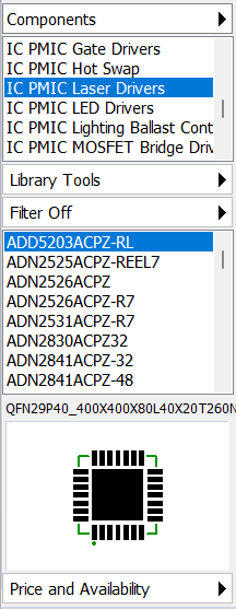
Price and Availability - check the selected component’s price and availability on the Mouser website or across our supplier database.
3.1.4. Design Manager
This panel is on the right side of the screen. To display/hide the Design Manager, select "View \ Toolbars \ Design Manager" from the main menu or press Ctrl+2 hotkeys by default.
There are three tabs in the upper part of the Design Manager.
Layers tab – change and manage board layers (add/move/delete/hide layers, change settings and layer display mode). Blue check marks – show/hide the layer, color rectangle – change the layer color. Double-click on the layer name to make this layer active.
Objects tab – show/hide different objects on the design area and block certain objects from being selected.
Properties tab – editable properties of selected tool/object.
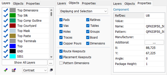
Right below is the Design Manager, it allows the designer to navigate through the layout. Press  button to see the list of components, and press
  button to see the list of nets. Select component or net in the list, and all pins of selected object will appear in the list right below. Left-click in that list to highlight an object, or double-click it in the list to pan the design area to selected object. You can right-click on any component, net or pint in the list to open its submenu.
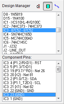
To adjust the width of the Design Manager panel, hover the mouse pointer over its edge, then drag and drop it.
3.1.5. Status Bar
Status bar is located in the bottommost part of the PCB Layout window.

It shows the following information:
Hint - depending on the selected option, displays standard or detailed pop-up hint (containing pad/via/hole dimensions, trace length) for the objects on the design area.
Mode - shows the current mode (Default, Route Manual, Edit Traces, etc.).
View - the current view (Normal, Mirror).
Grid Snap - the current Snap to Grid (link PCB Layout > View functions > Grid) status.
X, Y - coordinates of the current position of the cursor or selected element.
3.1.6. Main menu
3.1.6.1. File
New – create a new layout. If current project has unsaved changes, DipTrace will offer to save it. PCB Layout can open one project at a time. If you would like to open several layouts, for example, to copy objects between them, just run several instances of DipTrace PCB Layout.
Open – open existing layout (*.dip, *.dipxml) or schematic (*.dch, *.dchxml) file.
Open Recent – open 5 last layout projects.
Save – save current layout. If the project has never been saved, specify the file name in the pop-up dialog box, otherwise the project is automatically saved into the file. This tool is active only if a current layout has unsaved changes.
Save as – save layout into selected file.
Save Selected As – save selected objects into the file.
Import – import layout or its part from DipTrace ASCII, DipTrace XML, DXF, Gerber, N/C Drill, ODB++, Altium, Eagle XML, KiCAD, P-CAD ASCII, P-CAD PDIF, PADS ASCII, OrCAD Min, Sprint-Layout, Interchange, Autorouter SES as well as netlists from Accel, Allegro, Mentor, OrCAD, PADS, PCAD, KiCAD, Protel 2.0 and Tango formats.
Export – export layout to DipTrace ASCII, DipTrace XML, DXF, PDF, Gerber, Gerber X2, N/C Drill, ODB++, IPC-2581, IPC-D-356A, Bill of Materials, Pick and Place, G-Code for Solder Paste Dispensing, Mach 2/3 Drill, OrCAD TAP Drill, P-CAD ASCII, PADS PCB ASCII, OrCAD Min Interchange, Eagle XML and Autorouter DSN formats.
Order PCB – order PCB manufacturing with Bay Area Circuits (California), PCBWay (China) or Aisler (Netherlands).
Titles and Sheet Setup – Titles and Sheet Setup dialog box to set sheet size and orientation, border margins, titles, zones, and open the Title Block Editor.
Preview – preview and customize printing options (size, scale, colors, etc.) before printing.
Print – print current design. We recommend to print from the Print Preview panel. Sheet settings and titles are set in the Titles and Sheet Setup dialog box.
Layout Information – general information about the circuit board: current and a maximum number of pins, patterns, nets, vias, jumpers, holes, layers, routed nets, a length of traces, board width, height, total board area, and related schematic.
Update Layout from Schematic – synchronize the PCB layout with the source schematic file. New components, footprints, and nets are added automatically while preserving the existing board layout and routing whenever possible.
Update Layout from Netlist – update the PCB layout using an netlist file. Supported netlist formats include Accel, Allegro, Mentor, OrCAD, PADS, P-CAD, Protel, Tango, and KiCad.
Recover Board – recover the latest project. Use this feature when the program was incorrectly closed or the project was not saved for some reason. Recovery file is saved automatically every 10 steps.
Recovery Options – configure the recovery options: turn ON/OFF recovery and change number of steps to record.
Exit – close the PCB Layout. If current project has unsaved changes, DipTrace offers to save it.
3.1.6.2. Edit
Undo – one editing step backward.
Redo – one editing step forward. It is active only after Undo. If you edit the layout after using the Undo tool, the Redo becomes inactive.
Undo/ Redo Zoom – select if to consider Zoom a separate editing step or not.
Cut – move selected objects to the clipboard.
Copy – copy selected objects.
Paste – paste objects from the clipboard.
Delete – delete selected objects.
Select All – select all objects on the design area.
Edit Selection – select objects by type, layer, etc. automatically.
Cross Selection - enable cross selection between Schematic Capture and PCB Layout, choose objects and actions to be included in this function.
Find in Layout – find specified component or net on the layout. Search layout by full or partial RefDes, Value or Name.
Copy Matrix – create the matrix based on selected object/s. Specify the number of rows, columns and row/column spacings.
Keep RefDes while Pasting – keep all reference designators when pasting another layout. Select this option if panelizing different layouts on a single board.
Rotate – rotate selected objects 90 degrees counter-clockwise. If objects form a group, they have a common center of rotation. Otherwise, each has its own center of rotation.
Rotate Group – rotate selected objects around one common center point.
Flip Group – flip selected objects vertically and horizontally.
Align Objects – align selected objects horizontally or vertically and distribute them equally.
Radial Placement – place selected objects radially with defined placement center, radius, step or distribute them equally between specified circonference angles. The feature can be applied to components, pads, mounting holes, vias and fiducials.
Group – unite all selected objects into a group. This tool is active only if several objects are selected.
Ungroup – ungroup selected objects. This tool is active only if at least one group is selected.
Lock Selected – lock moving and editing of selected object/s.
Unlock Selected – unlock moving and editing of all selected objects, if they were previously locked.
Lock Components – lock moving and editing of all components on the top or bottom side of the board.
Properties – the properties of selected objects.
3.1.6.3. View
Toolbars – show/hide the toolbars.
Display Hint – select whether to show a standard or detailed pop-up hint (containing pad/via/hole dimensions, trace length) for the objects on the design area. The hint is always displayed in the bottom-left corner of the screen.
Place Component Preview – show component's footprint before placing it on the design area.
Component Markings – configure default component markings, font, location, etc.
Pad Markings – enable/disable the display of Pad Numbers, Net Names or both as markings of the pads.
Trace Markings – enable/disable the display of Net Markings showing the net names on the traces.
Move Component Texts (F10) – use this tool to move reference and other designators to desired position.
Objects – show/hide layout objects by types. All objects (except pattern dimensions) are visible by default.
Ratlines – optimize, show/hide ratlines (connections).
Component Fiducials – show/hide fiducials of the components containing them in the current project.
Add to Assembly – specify objects automatically included in Assembly layer (pads, component silkscreen, board outline, component borders).
Jumper Wires – change the layer for the jumper wires (silkscreen, assembly, signal, or don't show them at all).
Layer Display – change the layer display mode and the contrast level between active and inactive layers.
Mirror – mirror current board horizontally.
Flip Text Automatically – flip all texts on the bottom side of the board on the design area. This option does not flip texts when exporting the PCB for manufacturing.
Display Titles – show/hide the titles. Sheet settings and titles are set in the Titles and Sheet Setup dialog box.
Display Sheet – show/hide sheet contours. Sheet size is set in the Titles and Sheet Setup dialog box.
Scale – change the layout scale (from 25% to 800%, or type in a new value), use the mouse wheel or Plus sign (+) and Minus sign (-) keys.
Line Width – set default line width for silk layer, component and board outline, courtyard and other layers, tables and titles.
Colors – change PCB Layout color template and printing colors.
Graphics Mode – change the graphics mode for the design area.
Units – change measurement units (mm, mil or inches).
Precision – adjust precision rate for project values and the grid.
Display Origin – show/hide the design origin.
Define Origin – determine and origin with the mouse pointer or by coordinates.
Grid – show/hide grid.
Snap to Grid – enable/ disable snap to grid option, when the grid is on.
Grid Size – select the grid size (standard or custom).
Y Grid Size – separate grid step for the Y axis.
Customize Grid – edit standard and custom grid sizes.
3.1.6.4. Objects
Place Component – the Place Component dialog box.
Find Component – the search filters dialog box.
Search Parts at SnapMagic – search SnapMagic libraries directly from within DipTrace.
New Part Request – place an order to get the required part designed within 24 hours.
Place Ratline – create a logical connection (ratline) between two pads by left clicking them (new net will be created).
Place Pad – place pad tool. Specify default pad type and dimensions at the Properties tab on the Design Manager.
Place Static Via – place static via, via style is set at the Properties tab.
Via Tools - use this toolkit to add, remove or configure Via Stitching, Via Shielding, and Component Fanout.
Place Mounting Hole – place a mounting hole on the design area. Setup default hole parameters in the Properties tab of Layers/ Objects/ Properties panel.
Place Fiducial – place a fiducial on the design area. Set up X and Y coordinates as well as its default parameters (copper and keepout diameters) in the Properties tab of Layers/ Objects/ Properties panel.
Place Planar Inductor - create and place or save to New or Existing library a planar inductor with defined geometry input and output parameters.
Place Copper Pour – place copper pour on current signal layer.
Update All Copper Pours – update all copper pours on all layers of the board.
Clear All Copper Pours – unpour all copper pours on all layers of the board.
Place Board Outline – place the board outline.
Board Points – define points of the board outline polygon (precise editing).
Delete Board – delete the board polygon.
Place Dimension – place horizontal, vertical, free, or radial dimensions and pointers which can be exported to Gerber format.
Place Table – place table on the design area. The table can be in Assembly or Silk layers.
Reports – generate and place report tables directly in the design area, including Bill of Materials (BOM), Pick and Place, Layer Stackup, and Drill Sizes tables.
Place Shape – place a shape object (line, arc, rectangle, filled rectangle, ellipse, filled ellipse, polyline, filled polygon) to selected or current layer.
Place Text – place a text object.
Place Picture – place an image.
Place QR code – generate and place a QR code containing a URL or text information.
Drawing properties – change line width for new shapes and font properties for text objects. Shapes, pictures and text objects belong to a single type of objects.
Measure (Ruler) – measure distances on the layout. Left-click in the starting point and move the mouse pointer to the end point keeping left button pressed. The length appears in the lower-left corner of the screen as a hint. Object's key points highlight automatically.
3.1.6.5. Placement
Arrange Components – arrange all components next to the board outline (inside or outside). It's not component placement. This feature is used to arrange chaotic layout right after converting schematic to board.
Placement by List – place components manually from the list sorted by RefDes. Placed components (located inside the board outline) disappear from the list automatically.
Place Selected by List - select components in the Schematic and place them manually from the list generated in the PCB Layout. Make sure to enable Cross Selection and Highlight to use this function.
Radial placement – place selected objects radially with defined placement center, radius, step or distribute them equally between specified circonference angles. The feature can be applied to components, pads, mounting holes, vias and fiducials.
Run Auto-placement – auto-place all unlocked components and optimize the layout according to the length of connection lines between the pads. Works inside or outside the board outline (check Place Components Outside the Board Outline checkbox in the Placement Setup dialog box).
Auto-place Selected – auto-place only selected components.
Placement Setup – the Placement Setup dialog box. Change placement accuracy, X/Y spacings, and placement options.
BOM/ Interactive BOM - configure and place a BOM on the design.
3.1.6.6. Route
Run Autorouter – launch current autorouter.
Current Autorouter – select current autorouter and some autorouting settings.
Autorouter Setup – autorouter setup dialog box.
Electra/Specctra Interface – export layout to *.dsn format and import traces and layout from the *.ses file produced by external autorouter.
Manual Routing – manual routing tools:
Add Trace – route trace manually.
Edit Traces – edit existing traces with respect to 90 and 45 degrees angles. This mode is activates automatically when you try to edit trace in the Default mode. Select this tool if a trace lies under the component.
Free Edit Traces – edit existing traces by moving nodes and lines without restrictions.
Add Meander – edit existing traces by dragging and dropping, creating serpentine to increase trace length for length matching.
Interactive routing – enable Walk Around and/or Push Traces routing modes, configure interactive routing options, clearance handling, and jump over settings for Routing, Trace & Via Editing, and Object Editing.
Layer Setup – the Layer Setup dialog box: add/insert/delete layers, change their properties and rearrange them, layer stack manager. The Layers tab on the right side of the screen provides the same functionality.
Routing Setup – specify default routing parameters: trace width and clearance of default net class, default via style dimensions, and additional manual routing settings.
Via Styles – add/edit/delete via styles. Via styles host all via parameters.
Net Classes – add/edit/delete net classes. Trace width and clearance, detailed object to object clearances by layer, trace length limits, allowed via styles, autorouting parameters and differential pair settings.
Hierarchy – arrange components to hierarchy blocks directly on the board and apply placement and routing from one block to another. Works if source schematic had hierarchical structure.
Teardrops – set parameters of the teardrops for thought-hole and SMD pads, vias and net T- junctions applied to the selected or all existing objects of the layout.
Load Rules – load rules (all settings, layers, via styles, net classes, DRC constraints) from previously saved rule file (*.rul) or another layout (*.dip).
Save Rules – save rules (all current settings, layers, via styles, net classes, DRC constraints) into the rule file (*.rul).
Unroute Selected – unroute selected nets.
Unroute All – unroute all nets of the layout.
Connection Manager – the Connection Manager dialog box.
Trace Templates – manage (add/edit/delete/activate) trace templates.
Lock Net Structure – lock entire net structure to prevent accidental changes.
3.1.6.7. High Speed
Define Differential Pair – create a differential pair (specify nets, color, and net class parameters for the pair).
Differential Pair Manager – create new differential pairs, sort them by net classes, edit parameters of all existing differential pairs in a single dialog box.
Define Paired Pads – specify pad pairs for each net of a differential pair. This is helpful on very rare occasions if DipTrace terminates the differential pair on the wrong pads.
Differential Pair Tools – edit differential pair routing tools.
Edit Single Trace – edit single trace of a differential pair with respect to 45- and 90-degree angles.
Free Editing of Single Trace – edit single trace of a differential pair without any constraints.
Phase Tune – calculate phase shift between the tracks of a differential pair and apply custom and auto-sized meanders to compensate it.
Length Matching – set length/tolerance rules, and match the length of selected traces on the circuit board.
Add Meander – place meanders on the design area.
3.1.6.8. Verification
Check Design Rules – (DRC). This feature verifies current design according to the design rules/constraints and reports errors (trace crossings, small clearances, small/big sizes, etc.). The list of errors appears in the upper-right and allows the user to navigate through the layout and fix errors step-by-step.
Design Rules – specify the design rules and constraints. Turn ON and set up the Real-time DRC in this dialog box.
Hide Errors – hide design errors.
Check Net Connectivity – verify electrical connectivity of all nets of the project. Verification reports all isolated areas and pins. Traces, shapes, and copper pours are counted as connectors. Error description shows broken nets (nets with more than one area (pin/pins disconnected from the rest)).
Compare to Schematic – compare current layout to the source-schematic from the specified *.dch file. The list of differences is displayed in the upper-right corner. New patterns and nets added to the design directly in the PCB Layout are reported as errors (if schematic and layout are not in sync).
3.1.6.9. Library
Library Setup – the Library Setup dialog box allows the user to: add/delete component library groups, add new libraries from the separate files, and delete libraries from the groups.
Copy <Library> to another group – copy selected library (selected in the list on the Component placement panel) to another library group.
Open <Library> in Component Editor – open the current library (selected in the list on the Component placement panel) in the Component Editor.
Open <Library> in Pattern Editor – open the current library (selected in the list on the Component placement panel) in the Pattern Editor.
Add Library to <Library group> – add selected library to current library group.
Move <Library> to Another group – move selected library to another library group.
Remove <Library> from <Library group> – remove selected library from current library group.
Add project libraries from another project – add all libraries from another DipTrace project file.
Save Design Cache as library – save auto-generated Design Cache library as a regular library.
Clear Design Cache – remove all components from the Design Cache library (does not change the project itself).
Remove <Component> from the Design Cache – remove selected components from the Design Cache library.
3.1.6.10. Tools
RefDes Renumbering – arrange reference designators from the top-left of the circuit board to the bottom-right by rows or by columns.
3D Preview – preview the circuit board in real-time 3D and export the board model to STEP and VRML formats. 3D Models for components should be downloaded from the DipTrace website or from other online resources. Set the folder with 3D models in the "Tools \ 3D Preview \ Patterns and Models Search..." dialog box. Choose Graphics Mode for 3D preview of the board (Same as 2D, Direct 3D, Open GL).
Panelizing – create several copies of the PCB on a single panel, based on defined column/row count and spacings between the boards on the pane with V-scoring or Tab Routing options.
PCB Calculator - easily calculate trace width, clearance, current, resistance, transmission line characteristics, differential pairs impedance and more. Customize width, length, gap, and layer stackup manually or based on selected trace, differential pair and layer stackup settings. Adjust parameters and place planar inductors directly onto your layout or save them to the library for future use
Plugins - extend the software functionality by running plugins. Comprehensive documentation and plugin examples with source codes are provided.
Hotkey Settings – set up and change hotkeys for various dialog boxes and tools in DipTrace.
Environment Variables – define and manage environment variables.
Schematics – launch DipTrace Schematic module.
Pattern Editor – launch DipTrace Pattern Editor.
Component Editor – launch DipTrace Component Editor.
3.1.6.11. Help
PCB Layout Help – PCB Layout help file.
DipTrace Tutorial – DipTrace PDF step-by-step tutorial, learn how to work in DipTrace on simple examples.
Getting Started – the Getting Started dialog box with useful software links.
Register – register your DipTrace (enter the Username and Registration key of the purchased DipTrace edition).
Request Support – DipTrace Customer Support portal.
PCB Design Service – request affordable PCB design service from our experienced electronic engineers.
DipTrace Home Page - DipTrace on the web.
About – information about current DipTrace edition and version.
3.1.7. Object submenus
3.1.7.1. Component
To open this submenu, right-click on a component on the design area or in the list of components on the Design Manager panel.
<Component RefDes> – change component reference designator. Current RefDes is a caption.
Optimize RefDes – remove empty places in the RefDes numbering array, if some components were deleted.
RefDes Renumbering – arrange reference designators from the top-left to the bottom-right of the design by rows or by columns.
Links – open internet links from additional fields of selected component in default Internet browser.
Do Not Panelize – remove the pattern from the panelization.
Lock Selected – lock moving and editing of all selected objects.
Unlock Selected – unlock moving and editing of all selected objects, if they were previously locked.
Unlock Layer – unlock component side/layer (visible only if the layer is locked in the "Edit \ Lock Components \ ..." main menu item).
Change Side – change component side (applies to all selected components).
Connect Traces – connect component pads to trace ends placed at the same grid points.
Disconnect Traces – disconnect component pads from the traces.
Route Traces – route nets connected to pads of selected component.
Unroute Traces – unroute traces connected to the pads of the selected component.
Rotate – rotate selected object 90 degrees counter-clockwise. If objects form a group, they have a common center of rotation. Otherwise, each has its own center of rotation.
Rotate by Angle – rotation angle for selected object.
Free Rotate – visually rotate selected object to any angle with the mouse.
Radial Placement – place selected components radially with defined placement center, radius, step or or distribute them equally between specified circonference angles.
Hide Pad Rings in Layer – hide pad copper rings for selected components in the current signal layer. Autorouter will not connect traces to such pads on the layer where pads are hidden.
Show Pad Rings in Layer – show pad rings for selected components in current signal layer.
Fanout – set automatic via placement for the pads of SMD component.
Pad Signal Delay – define any additional distance that a signal propagates within a component. This value is considered for phase tuning and length matching.
Component Fiducials – select whether to apply fiducial display mode set for the entire project - Common State (defined via View/ Component Fiducials) or show/hide fiducial/s of the selected component.
Replace Component – replace the current component.
Update from Library – update pattern from the library to apply changes made in the Pattern Editor.
Save To Library – select library group and save selected pattern into a library (*.lib file).
Group into Component – group selected objects into a single pattern.
Ungroup Component – ungroup selected pattern to pads and shapes.
Pattern Origin – show/hide the origin of selected component.
Grid Alignment – select whether to align components By Pads or By Origin.
Snap to Grid – snap selected objects to the grid, when the grid is on, but Snap to Grid option is disabled for the overall project.
Cut – move selected objects to the clipboard.
Copy – copy selected objects to the clipboard.
Delete – delete selected objects.
Group – unite all selected objects to a group. The tool is active only if several objects are selected.
Ungroup – ungroup selected objects. This tool is active only if at least one group is selected.
3D Model – change attached 3D Model of the pattern.
Standard Pad Properties – change pad properties of the current component.
Properties – change the component properties.
3.1.7.2. Pad
To open this submenu right-click on a pad on the design area or in the list of pins on the Design Manager panel.
Pad Number – change the pad number.
Net Name – change the net name (if pad belongs to any net).
Diff Pair Name – change differential pair name (if pad belongs to a differential pair)
Trace Color – change the color of the pad's trace.
Diff Pair Color – change color of the differential pair.
Add to Net – add the current pad to any net from the list or visually.
Delete from Net – delete current pad from the net.
Route Net/Diff Pair – route pad's net or two nets of a differential pair.
Unroute Net/Diff Pair – unroute net of this pad or two nets of a differential pair.
Hide Net Ratlines – show/hide ratlines (connections) of the pad's net.
Delete Net – delete the pad's net.
Remove Differential Pair – remove differential pair declaration from the nets (the nets and traces remain).
Pad Layers – hide pad in certain layers and create blind or buried pads.
Hide Pad Ring in Layer – show/hide the pad ring in current signal layer (the hole remains in the layer).
Thermal Settings – select custom thermal settings for pads.
Teardrop – set parameters of teardrops for individual thought-hole and SMD pads or pads of the selected component/-s.
Mask/Paste Settings – define custom paste and mask settings for the pad.
Fanout – automatic via placement for current pad or connected net.
Signal Delay – define any additional distance that a signal propagates within a component. This value is considered for the phase tuning and length matching.
Show Trace Length – display the length of the trace directly on the design area.
Add to Length Matching – launch Length Matching tool and add connected net to the length comparison list.
Cut – move selected objects to the clipboard.
Copy – copy selected objects to the clipboard.
Delete – delete selected objects.
Net/Diff Pair Properties – change net properties or differential pair properties.
Define Paired Pads – define paired pads for differential pairs (on rare occasions when DipTrace terminates the differential pair on the wrong pads).
Pad Properties – change the pad properties.
3.1.7.3. Via
Right-click on a via to open this submenu.
Via RefDes – change via's reference designator.
Net Name – change the via's net name (if via belongs to some net).
Lock Selected – lock moving and editing of selected objects.
Radial Placement – place selected vias radially with defined placement center, radius, step or or distribute them equally between specified circonference angles.
Unlock Selected – unlock moving and editing of selected objects, if they were previously locked.
Add to Net – add current via to any net from the list or visually with the mouse.
Delete from Net – delete current via from the net.
Hide Net Ratlines – show/hide the ratlines (connections) of current via's net.
Connection Manager – the Connection Manager dialog box.
Connect Traces – connect via to the ends of traces located in the same point of the grid.
Disconnect Traces – disconnect via from the traces.
Convert to Trace Via – convert static via to dynamic (trace) via, which is technically part of the trace.
Convert Via to Static – convert trace (dynamic) via to static.
Hide Via Ring in Layer – show/hide via ring in the current signal layer.
Thermal Settings – define custom thermal settings for the via.
Teardrop – set parameters of teardrops for individual via or vias and pads of the selected objects.
Mask / Paste Settings – individual paste and mask settings for the via.
Cut – move selected objects to the clipboard.
Copy – copy selected objects to the clipboard.
Delete – delete selected objects.
Group – unite all selected objects to a group. The tool is active only if several objects are selected.
Ungroup – ungroup selected objects. This option is active if at least one group is selected.
Net Properties – change the net properties of the via's net.
Via Properties – change the via properties.
3.1.7.4. Mounting Hole
Right-click on any mounting hole to open this submenu.
<Mounting Hole RefDes> – change mounting hole reference designator. Current RefDes is a caption.
Lock Selected – lock moving and editing of all selected objects.
Unlock Selected – unlock moving and editing of all selected objects, if they were previously locked.
Align Objects – align selected object horizontally or vertically and distribute them equally.
Radial Placement – place selected mounting holes radially with defined placement center, radius, step or or distribute them equally between specified circonference angles.
Replace Component – replace the current mounting hole.
Save To Library – select library group and save selected pattern into a library (*.lib file).
Group into Component – group selected objects into a single pattern.
Snap to grid – snap selected objects to the grid, when the grid is on, but Snap to Grid option is disabled for the overall project.
Cut – move selected objects to the clipboard.
Copy – copy selected objects to the clipboard.
Delete – delete selected objects.
Group – unite all selected objects to a group. The tool is active only if several objects are selected.
Ungroup – ungroup selected objects. This tool is active only if at least one group is selected.
3D Model – change attached 3D Model of the pattern.
Properties – change hole position and diameters of the hole and keepout.
3.1.7.6. Net
To open this submenu, right-click on a net on the design area or in the list of nets on the Design Manager panel.
<Net Name> – change the net name.
Lock Selected – lock moving and editing of all selected objects.
Unlock Selected – unlock moving and editing of all selected objects, if they were previously locked.
Arc – remove or create an arc from trace segments.
Add Node – add node to the trace. Use the N hotkey by default.
Delete Node – delete current node from the trace.
Segment Width – select width of the trace segment. It can be custom or set by Net Class or by a template.
Trace Width – select width of the trace (use net class, template or a custom value).
Net Width – select width of the net (use net class,template or a custom value).
Teardrops – set parameters of teardrops for thought-hole and SMD pads, vias and T- junctions, belonging to the net or to all selected objects.
Segment Layer – move the current trace segment to another signal layer.
Trace Layer – move the current trace to another signal layer or make it a top or bottom jumper wire.
Net Layer – move current net to another signal layer.
Trace Color – define custom color for the traces and pads.
Show Trace Length – show the length of selected trace.
Length Matching – launch Length Matching tool and add selected nets to the length comparison list or compare just the length of selected nets.
Meander Gap – set custom or net-class gap between trace meanders.
Hide Net/Pair Ratlines – show/hide net/diff pair connections (ratlines).
Unroute Segment – unroute the trace segment.
Unroute Trace – unroute the trace.
Unroute Net – unroute selected net.
Delete Net – delete the selected net/-s.
Cut – move selected objects to the clipboard.
Copy – copy selected objects to the clipboard.
Delete (Del) – delete trace; net is maintained.
Group – unite all selected objects into a group. Tool is active only if several objects are selected.
Ungroup – ungroup selected objects. Tool is active only if one or more groups are selected.
Via Properties – via properties for current trace segment.
Net/Diff Pair Properties – net properties dialog box or differential pair properties dialog box.
3.1.7.7. Differential pair
Right-click on any differential pair trace to open this submenu.
<Diff Pair Name> – change the differential pair name.
Lock Selected – lock moving and editing of all selected objects.
Unlock Selected – unlock moving and editing of all selected objects, if they were previously locked.
Add Node – add a node to the trace. Use the N hotkey.
Delete Node – delete the current node from the trace.
Neck Segment – neck current segment of the differential pair according to the Necking parameters set by the Net Class.
Remove all Necks from Pair – remove all necking from selected differential pair.
Segment Layer – move current trace segment to another signal layer.
Trace Layer – move current trace to another signal layer.
Diff Pair Layer – move differential pair traces to another signal layer.
Diff Pair Color – define a custom color for differential pair traces and pads.
Show Trace Length – show the length of differential pair traces.
Length Matching – launch Length Matching tool and add nets of the differential pair to the length comparison list.
Meander Gap – set custom or net-class gap between trace meanders.
Hide Pair Ratlines – show/hide diff pair connections (ratlines).
Highlight Net – with this option enabled the selected net will be displayed as dotted line/ polyline/ curve.
Unroute Segment – unroute differential pair segment.
Unroute Trace – unroute differential pair traces.
Unroute Diff Pair – unroute selected diff pair.
Remove Diff Pair – remove differential pair declaration from the nets (the tracks remain).
Cut – move selected objects to the clipboard.
Copy – copy selected objects to the clipboard.
Delete – delete selected objects.
Group – unite all selected objects into a group. The tool is active only if several objects are selected.
Ungroup – ungroup selected objects. The tool is active only if one or more groups are selected.
Via Properties – via properties for current trace segment.
Define Paired Pads – define paired pads for a differential pair (on rare occasions if DipTrace terminates the differential pair on the wrong pads).
Diff Pair Properties – differential pair properties dialog box.
3.1.7.8. Shape
Right-click on any shape to open this submenu.
Convert to Board Outline – convert shape polygon to the board outline (available only if the shape is placed in Board Cutout layer).
Group into Component – group selected objects into a single component.
Do Not Panelize – disable panelization of selected shape (original shape remains).
Lock Selected – lock moving and editing of selected objects.
Unlock Selected – unlock moving and editing of selected objects, if they were previously locked.
Insert Point – insert point to the polyline or polygon.
Delete Point – delete a point from the polyline or polygon.
Rotate – rotate selected objects 90 degrees counter-clockwise. If objects form a group, they have a common center of rotation. Otherwise, each has its own center of rotation.
Define Angle – defines rotation angle for selected object.
Free Rotate – rotate selected object/s visually with the mouse.
Align Objects – align objects horizontally or vertically with defined distribution settings.
Cut – move selected object/s to the clipboard.
Copy – copy selected object/s.
Delete – delete selected object/s.
Group – unite all selected objects into a group. The tool is active only if several objects are selected.
Ungroup – ungroup selected objects. The tool is active only if one or more groups are selected.
Properties – change the shape properties.
3.1.7.11. QR Code
Right-click on a QR Code object to open this submenu.
Change QR Code – open the QR Code Properties dialog to modify the QR code content and settings, including the placement layer, rotation angle, anchor point and its coordinates.
Flip QR Code – mirror the selected QR code while preserving its content and properties.
Convert to Text – Convert the QR code into its embedded text or URL.
Lock Selected – lock moving and editing of selected objects.
Unlock Selected – unlock moving and editing of selected objects, if they were previously locked.
Rotate – rotate selected objects 90 degrees counter-clockwise. If objects form a group, they have a common center of rotation. Otherwise, each has its own center of rotation (anchor point). You can use R or Space hotkeys for the same purpose.
Rotate by Angle – select a preset angle of rotation or customize it.
Free Rotate – this option allows rotating selected object by any angle visually, with the software displaying angle value in real time.
Align Objects – align objects horizontally or vertically with defined distribution settings.
Snap to grid – snap selected text objects to grid, when the grid is on, but Snap to Grid option is disabled for the overall project.
Cut – move selected object/s to the clipboard.
Copy – copy selected object/s.
Delete – delete selected object/s.
Group – unite all selected objects into a group. The tool is active only if several objects are selected.
Ungroup – ungroup selected objects. The tool is active only if one or more groups are selected.
Properties – change QR Code properties.
3.1.7.12. Table
Right-click on any table on the design area to open this submenu.
Name – change table name.
Current Cell – change properties of the current table cell (text, alignment, font).
Do Not Panelize – disable panelization of selected table (original table remains).
Lock Selected – lock moving and editing of all selected objects.
Unlock Selected – unlock moving and editing of all selected objects, if they were previously locked.
Column Width – change column width.
Row Height – change row height.
Insert Column – insert a new column into the table.
Insert Row – insert a new row into the table.
Add Column – add a new column to the table.
Add Row – add a new row to the table.
Delete Column – delete the current column from the table.
Delete Row – delete the current row from the table.
Save to File – save table content into a separate Excel CSV or text file.
Rotate – rotate selected object/s 90 degrees counter-clockwise. If objects form a group, they have a common center of rotation. Otherwise, each has its own center of rotation.
Snap to grid – snap selected objects to grid, when the grid is on, but Snap to Grid option is disabled for the overall project.
Cut – move selected objects to the clipboard.
Copy – copy selected objects to the clipboard.
Delete – delete selected objects.
Group – unite all selected objects into a group. This tool is active only if several objects are selected.
Ungroup – ungroup selected objects. This tool is active only if one or more groups are selected.
Properties – change table properties.
3.1.7.13. Copper pour
Right-click on the copper pour border to open this submenu.
Update – update copper pour.
State – change copper pour state (poured, unpoured).
Change Layer – move selected copper pour to another PCB layer.
Do Not Panelize – disable panelization of selected copper pour (original pour remains).
Lock Selected – lock moving and editing of all selected objects.
Unlock Selected – unlock moving and editing of all selected objects, if they were previously locked.
Insert Point – insert point to the copper pour outline. New point's location is the location of the mouse pointer on the outline.
Delete Point – delete the point from the copper pour outline.
Rotate – rotate the object 90 degrees counter-clockwise. You can use R or Space hotkeys for the same purpose.
Rotate by Angle – select a preset angle of rotation or customize it.
Free Rotate – this option allows rotating selected object with the mouse by any angle visually, with the software displaying angle value in real time.
Via Stitching – this tool allows for connecting copper areas on different layers with vias.
Cut – move selected objects to the clipboard.
Copy – copy selected objects to the clipboard.
Delete – delete selected objects.
Group – unite all selected objects into a group. The tool is active only if several objects are selected.
Ungroup – ungroup selected objects. This tool is active only if one or more groups are selected.
Properties – change the copper pour's properties.
3.1.8. Modes of operation
Modes of operation in the DipTrace PCB Layout:
Basic modes
Default – is a default operational mode. It is activated on the start-up. To enable this mode from any other mode, you need to right-click on an empty space of the design area or press  on the Elements toolbar. This mode allows the designer to select and move objects and edit existing traces (respectively to 90- and 45-degree angles), change a size of the shapes, texts, and images, and edit the board outline by automatically switching to necessary operational mode after clicking on the object.
Place Pattern – select component on the Component Placement panel and place it on the design area or click  button to open the Place Component dialog box and select component there.
Place Ratline – go to "Objects \ Place Ratline" from the main menu or press  button on the Elements toolbar to enable this mode. Left-click on the first pad of the net, then click the second and so on. A new net will appear automatically as a thin blue connection line.
Place Pad, Static Via, Mounting Hole or Fiducial – select "Objects \ Place Pad," "Objects \ Place Static Via", "Objects \ Place Mounting Hole" or or "Objects \ Place Fiducial" from the main menu or press the corresponding buttons on the Elements toolbar to enable these modes.
Place Board Outline – select "Objects \ Place Board Outline" from the main menu or press  button on the Route toolbar. Define the board polygon points with left clicks on the design area, then right-click, and select Enter from the submenu or hit Enter key.
Place Copper Pour – select "Objects \ Place Copper Pour" from the main menu or press  button on the Elements toolbar. Place copper pour on current signal layer by specifying the copper polygon points. Right-click, and select Enter from the submenu or hit Enter key when done – the Copper Pour Properties dialog box pops up.
Place Shape – select the shape, text or picture placement tool from the main menu ("Objects \ Place Shape, "Objects \ Place Text" or "Objects \ Place Picture") or on the Drawing toolbar.
Place Table – select "Objects \ Place Table" from the main menu or press  button on the Elements toolbar to enable this mode.
Routing modes
Route Manual – select "Route \ Manual Routing \ Add Trace" from the main menu, press  button on the Route toolbar or Tilde key (~) to enable this mode. Left-click on the pad or a trace segment, and then specify the key points of the trace all the way to the terminal pad. Change the current segment, width and other parameters on the Routing panel (left-hand side of the screen).
Edit Traces – select "Route \ Manual Routing \ Edit Traces" from the main menu or press  button on the Route toolbar. This mode allows the user to move trace segments with respect to 90- and 45-degree angles. When applied to a differential pair, this mode allows for moving two tracks simultaneously respecting the gap between the traces.
Free Edit Traces – select "Route \ Manual Routing \ Free Edit Traces" from the main menu or press  button on the Route toolbar to enable this mode. It allows the designer to move trace segments and nodes without any limitations. When applied to a differential pair, this mode allows for moving two tracks simultaneously respecting the gap between the traces.
Edit single trace of a pair ( button on the High Speed toolbar) and Free editing of a single trace (
 button on the High Speed toolbar) modes are used for editing a single track of a differential pair. They act as Edit Traces and Free Edit Traces modes if applied to a trace that is not in a differential pair.
Add Meander – select "High Speed \ Add Meander" from the main menu or press  on the High Speed toolbar. This mode allows for adding meanders to any traces on the design area. Phase Tune mode is essentially the same as Add Meander mode but applied only to differential pairs.
Other modes
Move Component Markings – select "View \ Move Component Texts" from the main menu or press the F10 key to enable this mode. It allows the designer to move component markings separately of their components anywhere on the board. Press R or Space hotkeys to rotate the markings while moving them.
Free Rotate – rotate selected objects visually with the mouse pointer. Right-click on the object, and select Free Rotate from the submenu.
Place Dimension – select "Objects \ Place Dimension \ <Dimension type>" from the main menu or press  button on the Elements toolbar. The object key points are highlighted, and you can attach dimension to any of these points, attached dimensions are automatically moved and recounted when you move/edit the objects.
Measure – measure selected spacing while designing the PCB. To activate this mode you need to press  button on the Elements toolbar, and left-click on the start point of the spacing, and move the cursor to the end point. The length of the spacing appears in the lower-left corner of the screen.
Define Origin – move the design origin. To activate this mode, select "View \ Define Origin \ By Mouse Pointer" from the main menu or press  button on the Elements toolbar. Then left-click on the design area to define a new origin's point.
3.1.9. Hotkeys
DipTrace features customizable hotkeys in all software modules. To open the HotKey Settings dialog box, proceed to "Tools \ HotKey Settings" from the main menu in any of the DipTrace modules: Schematic, PCB Layout, Component and Pattern Editors. The designer can view or assign custom keyboard shortcuts for various tools, actions, and dialog boxes by left clicking in the corresponding field and pressing a keyboard combination.
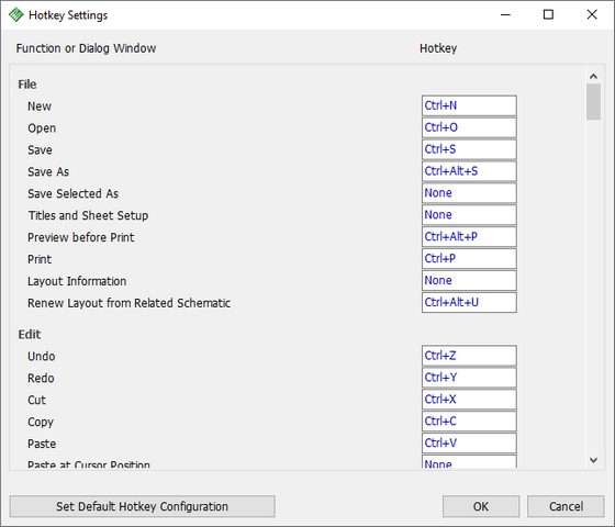
If a combination is already in use, a warning message appears. Notice that certain shortcuts are reserved by the program and are not customizable. Press OK to apply changes. To restore default configuration, press Set Default Hotkey Configuration button on the panel.
Hotkeys reserved by the system:
Ctrl Shift Shift + mouse 1 – 0 numbers Enter Esc Left arrow Right arrow Up arrow Down arrow Shift + S Shift+I Shift+P Alt+any key Tab |
– hold down to invert selection; – hold down to add objects to selection; – orthogonal moving of selected objects; – select corresponding PCB layer; – complete action; – cancel action; – move object left, pan left while routing/building; – move object right, pan right while routing/building; – move object up, pan up while routing/building; – move object down, pan down while routing/building; – enable disable auto-panning; – ON / OFF automatic check for new PCB Creator versions; – reserved by the system; – reserved by the system. – with a trace segment selected use Tab key to toggle between the selection of a segment, trace and net. The function can be applied to various traces/ nets simultaneously. |
3.1.10. Environment Variables
According to DipTrace License Policy, the software can be used by one license holder on several devices. To ensure smooth portability of your projects, DipTrace features an Environment Variables tool that allows setting variables for the paths to directories containing libraries, 3D models, images, etc. on different machines.
Go to Tools/ Environment Variables to open the Environment Variables dialog.
In the Common Variables section you can see the paths used by the software during installation and the corresponding variables for those paths.
In the User Variables part you can establish new variables for the paths to the directories, where your libraries or 3D models are stored. Type the variable in the Variable cell and set the path in the Folder line or press  button and select Browse for Folder to select the directory. Use the same variable on another PC to associate it with the path to the required folder on that machine. In this way when switching between machines the software will look for the files using the path corresponding to the established variable on the given PC.
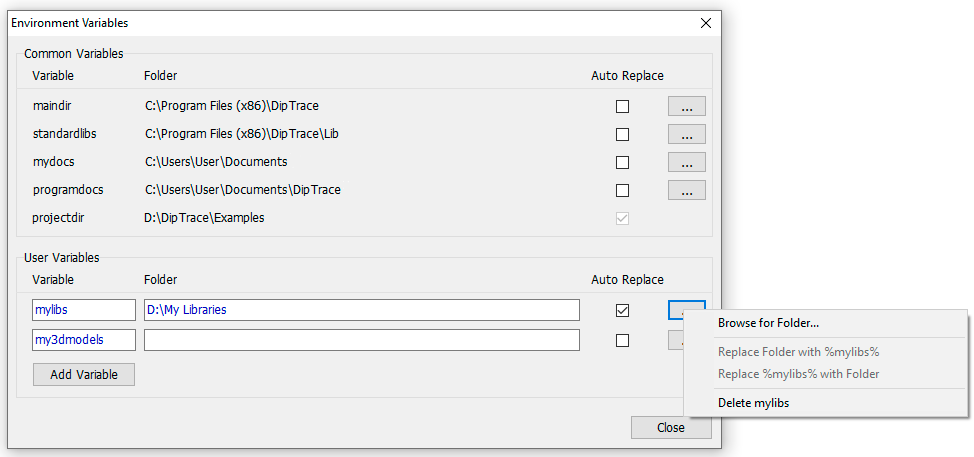
You can check the Auto Replace option for the software to substitute the path with the variable in any items with such path as soon as they appear in the project or press button and select “Replace folder with %variable name%” to apply this command to all currently existing items in the project. To reverse the command select “Replace %variable name% with Folder” from the menu.
Remember to use the same variables to set the paths to the corresponding folders on another machine. If your component or 3D model libraries have been changed, make sure to update them in the source folder on your device.
To delete a variable press and select Delete <Variable Name>.
Environment Variables feature also allows creating a portable version of the program by establishing a variable for the launch directory, which can be stored, for instance, on a portable drive.
3.2. Working with files
3.2.1. Create a circuit board
Launching the program (no command prompt) creates a new board automatically. To create a new PCB in the PCB Layout, select "File \ New" from the main menu or press the corresponding button on the Standard toolbar. If currently opened PCB has unsaved changes, DipTrace will offer to save it.
For a new board, you can use rules (settings, layers, via styles, net classes, DRC rules etc.) of any previously designed layout (*.dip or *.rul file). Rules can also be loaded with "Route \ Load Rules" main menu item after placement. Just make sure you import the rules before routing the nets.
3.2.2. Open PCB
Select "File \ Open" from the main menu or press the corresponding button on the Standard toolbar, and choose layout or schematic file (*.dip or *.dch).
When you open a schematic file, the layout of components may seem chaotic, use Arrange Components tool.
Go to "File \ Open Recent" from the main menu to open one of the five recent files.
3.2.3. Save PCB
Select "File \ Save" or "File \ Save as" from the main menu to save current project.
To save a project, select "File \ Save" from the main menu or press the corresponding button on the Standard toolbar. If the layout has never been saved, the Save As dialog box will pop up. The user should select a location and define the file name, all further changes will be rewritten automatically into selected file.
You can use the Save As tool to backup project into a separate file.
If you need to save only a part of your layout, select that part and choose "File \ Save Selected As" from the main menu.
3.2.4. Update Layout from schematic
If you made changes in the schematic, you need to update the PCB to keep schematic and layout synchronized. In DipTrace PCB Layout select "File \ Renew Layout from Schematic" from the main menu, and select either to renew By Components or By RefDes, then specify the schematic file.
Updating algorithm finds related components in the PCB Layout and Schematic then adds missing components and updates the netlist. Components locked in Schematic are ignored by the algorithm.
There are two basic ways of renewing a design from a schematic:
1. By Components – DipTrace compares unique hidden identifiers of the components, which are assigned in the Schematic. These IDs are static and hidden from the user. Component reference designators can differ on the layout and schematic.
Notice that By Components method does not work if the principal circuit was designed in other CAD program.
2. By RefDes – DipTrace finds related components in the PCB layout and the Schematic by their reference designators (RefDes). This method works even if a PCB and schematic were designed separately in different CAD software. The reference designators should be the same in schematic and on the board.
Notice that after the first update By RefDes, PCB hidden IDs will be assigned and further updates can be made By Components, allowing to change the reference designators.
New components are placed to the right, next to the board outline. Existing layout and routing remain if no changes were made.
By Related Schematic – technically it is not a different update mode, it updates layout By Components from the related schematic. The only advantage is that you don't need to select the source schematic file each time you update the layout. You can go to "File \ Layout Information" to view and assign related schematic file.
Note that you can lock components added or edited directly in PCB before renewing from Schematic. DipTrace will ask you to confirm their update based on Schematic. Press NO, if want to keep them unchanged.
3.2.5. Update Layout from Netlist
DipTrace allows updating layout from the netlist generated in one of the most common PCB design tools (Accel, Allegro, Mentor, OrCad, PADS, P-CAD, Protel, Tango).
To update your PCB from the netlist go to File/ Update Layout from Netlist/ <netlist format>. Browse for the netlist file and open it. The following dialog box will pop up:
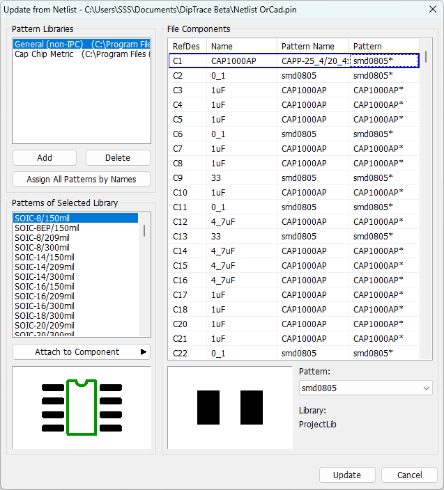
First, add the pattern libraries, use Add/Delete buttons, while holding Shift or Ctrl keys to select multiple libraries. Then press Assign all Patterns by Names, and DipTrace will find and attach all patterns with the matching names to the components.
Verify all patterns using the File Components list and preview fields right below for inspection. The Pattern Name column displays a component pattern from the netlist, while the Pattern column shows a corresponding pattern in the DipTrace library (if available).
Sometimes, the program can not find corresponding patterns due to the difference in the names. In such case, the user has to assign patterns manually. Select component in the list, then choose the pattern from the library, and press Attach to Component button. This allows to attach patterns to components according to their RefDes, name or pattern name.
The asterisk symbol (*) after the name of any pattern in the list indicates that the pattern has been connected manually.
Once all components have the correct patterns assigned, click the Import button.
New components will appear on the right side of the board outline.
3.2.6. Import
3.2.6.1. DipTrace ASCII
DipTrace allows you to save/open data in the textual DipTrace ASCII format. This format has been developed to allow for data transferring from/to other EDA packages and for forward compatibility between the DipTrace versions.
To import DipTrace ASCII-formatted library file, select "Library \ Import \ DipTrace ASCII" then select file, and click OK.
3.2.6.2. DXF
DipTrace allows the designer to import entire board layout or any part from DXF files.
To import DXF file, select "File \ Import \ DXF" from the main menu, and select a DXF file.
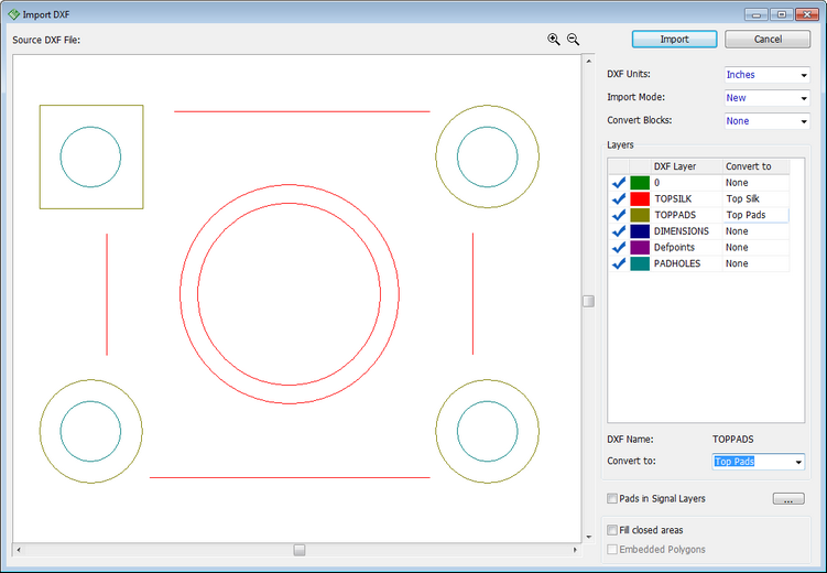
Use "DXF Units" drop-down to select the units (inches, millimeters, mils), in which the .dxf file was saved.
If "Import Mode: New" is selected, the software will create a new project. If "Import Mode: Add" is set, then the software will add objects to existing layout. You need to assign each DXF layer with an actual PCB layer. To specify DXF-to-PCB layer connections, select DXF layer, and then select proper PCB Layer from the Convert to drop-down list. To show/hide different layers of the DXF file, click on the blue check marks in the Layers list.
Notice that DipTrace currently does not support splines in DXF files. If you have DXF import related issues, most probably these were caused by DXF splines. Convert splines to regular polygons before importing the DXF file in DipTrace.
Recognize pads from the DXF
DipTrace can automatically recognize objects from the DXF drawings. For example, if pad shapes are in one DXF layer and all drills (including the mounting holes) in another DXF layer, specify "Convert to: Pads" for the first layer, and "Convert to: All Holes" for the second layer. You will get through pads (holes inside the pad shapes), surface pads (shapes without holes), and mounting holes (holes without shapes).
If pads, traces, and other objects are on a single DXF layer, you can automatically recognize pads, just check Pads in Signal Layers box, then click button to specify possible shapes and sizes of the pads.
Fill closed areas
Many DXF files require the filling of closed areas (formed by lines, arcs, polylines, rectangles, etc.). Check Fill closed areas box, and DipTrace will recognize closed areas and convert them to filled polygons. If you have several embedded areas (for example, characters inside pads or holes inside closed areas), check Embedded Polygons box. In this case, an outer, 3rd, 5th, etc. embedding will be filled, 2nd, 4th... etc. will become an empty area in the previously filled polygon.
DXF blocks can be converted to groups or components. If there are no blocks in the DXF file, you can group pads and shapes into a component after importing them using Group into Component item from the pad or shape submenu on the design area.
3.2.6.3. Gerber
DipTrace can import files in Gerber RS-274X or Gerber X2 format. Create all respective PCB layers to hold the Gerbers, then select "File \ Import \ Gerber" from the main menu and specify one or several Gerber files that you want to import (DipTrace also supports multi-layer Gerbers). The following dialog box will appear:
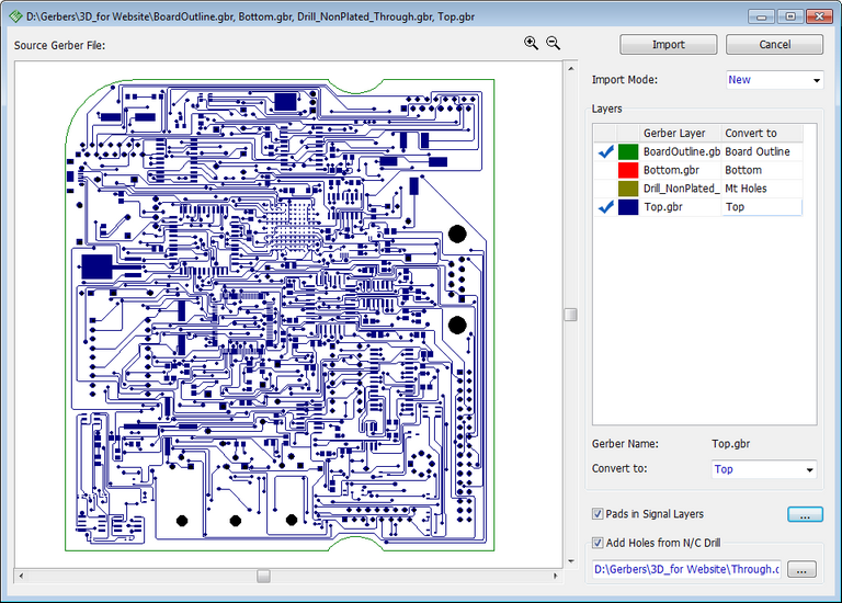
The key principles of the Gerber import interface are similar to the DXF import. To the right of the Gerber preview, there is instruments panel. If "Import Mode: New" is selected, the software will create a new project. If "Import Mode: Add" is set, then DipTrace will add the imported layout to existing one. You can import all or several layers (files) by checking/unchecking them in the Layers list.
Assign correct PCB layer to each Gerber file/layer that you want to import. Just select it from the Convert to drop-down list. If there are pads in the signal layer, check Pads in signal layer box. Use button to set possible shapes that will be considered as pads, however, default settings usually work well.
Gerber Import can be combined with N/C Drill Import, check Add Holes from N/C Drill, and specify the N/C drill file. The holes will also appear in the preview. Drills over pads will create through pads, and free drills will be converted to mounting holes.
Notice that only through N/C Drill holes are supported in Gerber Import dialog box. If you need to import blind or buried holes, please use the N/C Drill Import dialog box.
Click Import to proceed, or Cancel to reject import.
Notice that some CAD programs use negative Gerber layers. We recommend converting them to normal/positive type before importing them into DipTrace. The corresponding tools are widely available on the internet.
3.2.6.4. N/C Drill (Excellon)
To import an N/C Drill file, select "File \ Import \ N/C Drill" from the main menu, and select the file to import. The following dialog box will pop up:
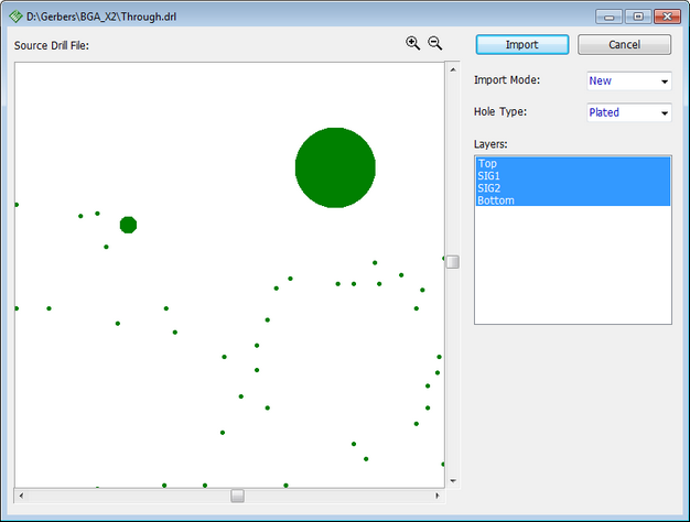
There are buttons to modify the import settings right next to the preview area. If "Import Mode: New" is set, a new project will appear. If "Import Mode: Add" is set, then the software will add the drills to existing layout.
Select correct PCB layers for each type of the holes. If all layers are selected, you will import through holes.
Use Ctrl key to specify only the layers of the blind or buried holes to import them. For example, if you have blind holes from Top layer to SIG2 layer, you need to select Top, SIG1, and SIG2 layers.
If you select only one layer, you will get through-hole pads available only in selected layer and hidden in all other layers.
Notice that only through mounting holes (non-plated holes) are allowed.
Click Import button to complete the import or Cancel to reject it.
3.2.6.5. ODB++
To import an ODB++ file, select "File \ Import \ ODB++" from the main menu. The following dialog box will appear:
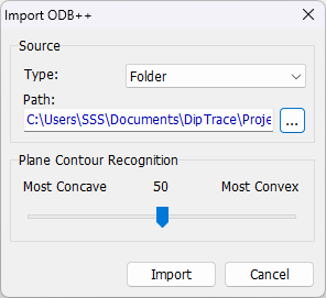
Choose the source type: compressed or simple folder to import and enter the path manually or press  to browse for the source folder.
Adjust plane contour recognition as needed and click Import.
In the next pop-up dialog choose ODB++ step and Layers to be imported.
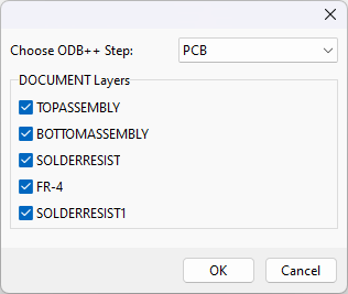
3.2.6.6. Altium ASCII
DipTrace imports PCBs from the Altium ASCII (*.pcbdoc) format.
Notice that PCB should be in the ASCII format, not binary (save PCB as an ASCII file in the Altium software).
In the DipTrace PCB Layout select "File \ Import \ Altium ASCII" from the main menu and open Altium ASCII PCB file. All components of an imported project are available in the auto-generated Design Cache library in the Project Libraries library group on the Place Component panel. You can save Design Cache as a regular pattern library directly on the Place Component panel or import component and pattern libraries from Altium in DipTrace Component Editor and DipTrace Pattern Editor.
3.2.6.7. Eagle PCB
DipTrace imports PCBs from the EAGLE format (*.brd).
Select "File \ Import \ EAGLE Board" from the main menu in the DipTrace PCB Layout, and select EAGLE PCB file (*.brd).
All components of an imported project are available in the auto-generated Design Cache library in the Project Libraries library group on the Place Component panel. You can save Design Cache as a regular library directly on the Place Component panel or import component and pattern libraries from EAGLE in DipTrace Component Editor and DipTrace Pattern Editor.
3.2.6.8. EasyEDA Pro
DipTrace supports import of PCBs from EasyEDA Pro format (*.epro).
Select "File \ Import \ EasyEDA Pro" from the main menu in the DipTrace PCB Layout, and select EasyEDA Pro project file (*.epro).
3.2.6.9. KiCAD
DipTrace imports PCBs from KiCAD format (*.kicad_pcb).
Select "File \ Import \ KiCAD board" from the main menu in the DipTrace PCB Layout, and select KiCAD PCB file (*.kicad_pcb).
All components of an imported project are available in the auto-generated Design Cache library in the Project Libraries library group on the Place Component panel. You can save Design Cache as a regular library directly on the Place Component panel or import component and pattern libraries from KiCAD in DipTrace Component Editor and DipTrace Pattern Editor.
3.2.6.10. OrCAD Min Interchange
DipTrace imports PCB layouts from the OrCAD Min Interchange format (*.min).
Select "File \ Import \ OrCAD Min Interchange" from the main menu, then open a *.min PCB file.
Notice that layout should be in the ASCII (*.min) format, not in the native binary OrCAD file.
Some minor differences are still possible between original OrCAD files and imported layouts (silkscreen texts, non-signal layers, unpoured copper pours). Please check all these in DipTrace before manufacturing.
3.2.6.11. P-CAD ASCII
DipTrace imports PCB layouts from the P-CAD ASCII (*.pcb) format.
Select "File \ Import \ P-CAD ASCII" from the main menu, then open a P-CAD PCB file.
Notice that the layout should be in the ASCII format, not in the P-CAD binary (both have the same extension in P-CAD).
3.2.6.12. P-CAD PDIF
PCB Layout allows the designer to import PCB files from the P-CAD PCB PDIF format.
Select "File \ Import \ P-CAD PDIF" from the main menu, then open PDIF file (*.pdf).
Notice that Adobe Acrobat PDF and PDIF are different formats with the same extension.
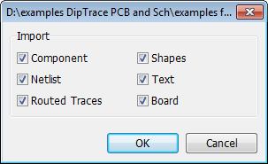
In the pop-up dialog box specify the objects to import, for example, if you don't need routed traces and shapes, but would like to import components and the netlist to route the board in DipTrace, check Components and Netlist boxes only. Click OK to convert PDIF file to DipTrace PCB Layout.
3.2.6.13. PADS ASCII 2005
DipTrace imports layouts from the PADS ASCII 2005 (*.asc) format.
Select "File \ Import\ PADS PCB ASCII 2005" from the main menu, then open PADS PCB file.
Notice that PADS layout should be in the ASCII (.asc) format, not in the binary.
Some minor differences are possible between original PADS layout and the imported one (silkscreen, non-signal layers, copper pours may be unpoured). Please check all these imperfections in DipTrace before ordering the PCB manufacturing.
3.2.6.14. Pulsonix
DipTrace supports import of PCBs from Pulsonix format (*.ppa).
Select "File \ Import \ Pulsonix" from the main menu in the DipTrace PCB Layout, and select Pulsonix PCB file (*.ppa).
3.2.6.15. Sprint-Layout 6.0 Text IO
DipTrace imports PCBs from the Sprint-Layout in text format.
Go to "File\ Import\ Sprint-Layout 6.0 Text IO" from the main menu in the DipTrace PCB Layout, and select the PCB file in text format (*.txt).
To save the project from Sprint-Layout 6.0 in text format go to Extras\ Text-IO: Export elements.
All components of an imported project are available in the auto-generated Design Cache library in the Project Libraries library group on the Place Component panel. You can save Design Cache as a regular library directly on the Place Component panel.
Note that footprints have to be represented as components, not as grouped objects in the Sprint-Layout project to be imported as such and clustered into a library in DipTrace PCB Layout.
Text objects may appear displaced in the imported project due to format differences. You can drag and drop the text to adjust its position.
3.2.6.16. Autorouter SES
DipTrace allows for external automatic routing with Electra and Specctra autorouters. Export DipTrace project to *.dsn format, route it with Electra or Specctra, and import results in the *.ses format back to DipTrace PCB Layout.
Select "File \ Import \ Autorouter SES", and select the file created by Electra or Specctra autorouters.
It is important to keep a source *.dip file open while autorouting and importing the *.ses file. Import process can take several seconds, depending on the project's complexity. Do not make any changes after you have exported DSN file and have not imported an SES file yet.
3.2.6.17. Netlist
PCB Layout allows the user to import netlists from the following formats: Accel, Allegro, KiCAD, Mentor, OrCAD, PADS, P-CAD, Protel, Tango. Select "File \ Import \ Netlist \ <netlist format>" and select the netlist file. The following dialog box will pop up:
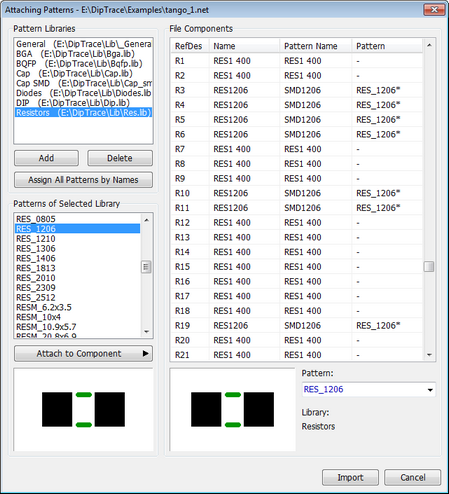
The first step is adding the pattern libraries, use Add/Delete buttons with Shift or Ctrl keys to select several libraries. Then press Assign all Patterns by names, and DipTrace will find and attach all patterns with the corresponding names to the components.
Check all patterns manually, use the File Components list, and preview fields right below for inspection. The Pattern Name column shows a component pattern from the netlist, and the Pattern column shows a respective pattern in the DipTrace library (if there is some).
Sometimes the program can not find corresponding patterns, because of the different names. In this case, the user assigns patterns manually. Select component in the list, then select pattern from the library, and press Attach to Component button, which allows the designer to attach patterns to components according to their RefDes, name or pattern name.
The Star symbol (*) after the name of any pattern in the list means that this pattern has been connected manually.
Click the Import button when all components have correct patterns.
3.2.6.18. 3DS, STEP, VRML, IGES
Each component of a circuit board requires a 3D model in order to properly work in DipTrace PCB Layout 3D Preview & Export module ("Tools \ 3D Preview \ 3D Visualization" from the main menu). DipTrace allows the designer to import externally designed 3D component models from STEP, VRML, 3DS, and IGES formats.
Go to "Tools \ 3D Preview \ Pattern and Model Search..." in order to set up the pattern search options and define folders with 3D models for automatic model search.
Right-click on a pattern on the design area, and select 3D Model from the submenu in order to assign or edit the attachment of a 3D model. However, we recommend assigning 3D models in the Pattern Editor.
3.2.7. Export
3.2.7.1. DipTrace ASCII
DipTrace allows the user to export data to the textual DipTrace ASCII format. This format was developed for forward compatibility.
To export layout file to DipTrace ASCII format, select "File \ Export \ DipTrace ASCII" in the DipTrace PCB Layout, define filename, and click OK.
3.2.7.2. DXF
To export a circuit board to AutoCAD DXF format, select "File \ Export \ DXF" from the main menu.
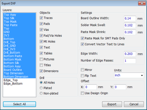
In the pop-up dialog box, you can select PCB layers and define objects which will be included in the DXF file. All PCB layers will become logical layers of the DXF file. Objects are saved as sets of entities.
There are two ways to export vector text: as AutoCAD text object or as polylines (Convert Vector Text to Lines checkbox). In the second case, the text will be exactly the same as in DipTrace, but you will not be able to edit it in AutoCAD.
Milling the PCBs
For PCB production with milling method, export Edge layer/s to the DXF (Edge_Top and/or Edge_Bottom layers). These layers have automatically generated edges for traces. Then generate G-code from the DXF edge polylines in special software, for example, Ace Converter, FlatCAM or other.
3.2.7.3. Gerber RS-274X
To export a circuit board to Gerber RS-274X format, select "File \ Export \ Gerber" from the main menu.
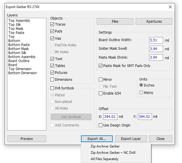
In the pop-up dialog box, select layer and define Objects that will be included or excluded in this layer by checking corresponding items. To preview each layer, select it, and click Preview.
Notice that settings are saved on the per-layer basis and should be defined only once (they will be restored even after restarting the program).
Export All button allows the designer to export all layers into a zip archive or separately as well as to add an NC Drill file to the archive.
In the Gerber Export dialog box, the user can change default solder mask swell and paste mask shrink values.
If you need to change names or extensions of Gerber files, press the Files button. In the pop-up dialog box, you can also include or exclude certain layers from being exported and set file arrangement options that are applied when you press the Export All button.
To mirror a Gerber layer, check the Mirror box. Flip Text option is disabled if "View \ Flip Text automatically" main menu item is checked. Offset is the shift of zero points from the bottom-left corner of the circuit board. You can use current design origin while exporting Gerber by checking the Use Design Origin checkbox. Set Recognition Accuracy for TrueType fonts, text in tables and raster pictures. Component Markings are automatically placed in the silk layers, text and pictures can be placed on any layer depending on their properties. Tables can be placed on silk or assembly layers.
PCB houses require drill files in the N/C Excellon format and Gerber files for manufacturing circuit boards. Find out more about N/C Drill export.
3.2.7.3.1. Drill symbols RS-274X
While most manufacturers require N/C Drill Excellon files, some quick-turn suppliers accept Drill Symbols in the Gerber format or use these files as additional means of quality assurance.
To export drill symbols, check Drill Symbols box in the Export Gerber RS-274X dialog box, make sure that all copper layers are selected in order to export through holes (should be selected by default), then select whether to export Plated, Non-Plated or All Holes, and press the Set Symbols button.
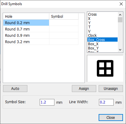
Select hole in the table, then select a symbol from the list, and use Assign or Unassign buttons. You can also change line width and symbol size if you need. Automatically assigned symbols work just fine in most cases, press Auto to assign symbols automatically. Press Close, and then press Export in the Export Gerber RS-274X dialog box to save selected holes as drill symbols.
Check Add Comments checkbox in the Export Gerber RS-274X dialog box to add drill symbols table to the right side of the hole layout.
If there are blind/buried holes on the circuit board, select a layer pair (top and bottom layer of the hole type), and repeat the procedure.
3.2.7.4. Gerber X2
To export a layout to Gerber X2 format, select "File \ Export \ Gerber X2" from the main menu.
Since Gerber X2 is compatible with Gerber RS-274X the dialog boxes are very identical with the only difference being the export of holes. Gerber X2 saves comprehensive drill layout in a Gerber-formatted file (not just Drill Symbols, like with Gerber RS-274X). Holes are automatically sorted by types and exported in the corresponding Gerber files. Gerber X2 also stores information about board stackup and layer functions, this significantly reduces the hassle when ordering PCB manufacturing.
In the pop-up dialog box, select a layer, and define Objects that will be included or excluded in this layer by checking the corresponding items. To preview each layer, select it, and click Preview.
Notice that settings are saved on the per-layer basis and should be defined only once (they will be restored even after restarting the program).
Export All button allows the designer to export all layers into a zip archive or separately as well as to add an NC Drill file to the archive.
In the Gerber Export dialog box, the user can change default solder mask swell and paste mask shrink values.
If you need to change names or extensions of Gerber files, press Files button. In the pop-up dialog box, you can also include or exclude certain layers from being exported and set file arrangement options that are applied when you press the Export All button.
To mirror Gerber layer, check the Mirror box. Flip Text option is disabled if "View \ Flip Text automatically" main menu item is checked. Offset is the shift of zero points from the bottom-left corner of the board. You can use current design origin while exporting Gerber by checking the Use Design Origin box. Set Recognition Accuracy for TrueType fonts, text in tables and raster pictures. Component Markings are automatically placed in the silk layers, text and pictures can be placed on any layer depending on their properties. Tables can be placed in silk or assembly layers.
Notice that despite comprehensive hole description in the Gerber X2 format, most PCB houses typically require drill files in the Excellon N/C Drill format.
3.2.7.5. N/C Drill (Excellon)
Most manufacturers require Excellon N/C Drill files to drill holes in a circuit board. To export a PCB to N/C Drill format, select "File \ Export \ N/C Drill" from the main menu.
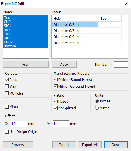
In the pop-up dialog box, select Objects which will be exported. After selecting objects, fill out the list of Tools being used. You can assign tools manually by typing in the tool number in the Number: T field or press Auto to assign tools automatically.
If you want to change default names or extensions of NC Drill files, press Files button.
Press Export All and DipTrace will determine all types of holes automatically and export all necessary files for each type of holes at a time. The user doesn't need to remember parameters of different via styles. Names of exported files consist of names of the top and bottom layer of the current hole type, the names are generated automatically (for example, "Through.drl" or "Top-Inner1.drl", etc.).
Offset is a shift of the zero point from the bottom-left corner of the board. You can use current design origin while exporting the N/C Drill by checking the Use Design Origin box.
Notice that the offset value for N/C Drill files and Gerber files should be the same. Otherwise, this can cause errors on the manufacturing stage.
To mirror the layout, check the Mirror box. To preview the N/C Drill file, select layers, and press the Preview button. Uncheck Plated and Non-Plated items to save plated and non-plated holes separately. Change the measurement units from inches to metric by checking the corresponding item.
If you want to save only the certain type of the holes, select all layers in order to export the through holes, for blind/buried holes select only the layer pair (top and bottom layer of the hole type). Use Ctrl or Shift keys to select several layers. Then press Export to save the file.
3.2.7.6. ODB++
ODB++ is a comprehensive CAD-CAM data exchange format which carries information about conductor layer artwork, drill data, layer materials and stack, test netlist, bill of materials, placement, fabrication data, dimensions, and more. Select "File \ Export \ ODB++" from the main menu in the PCB Layout.
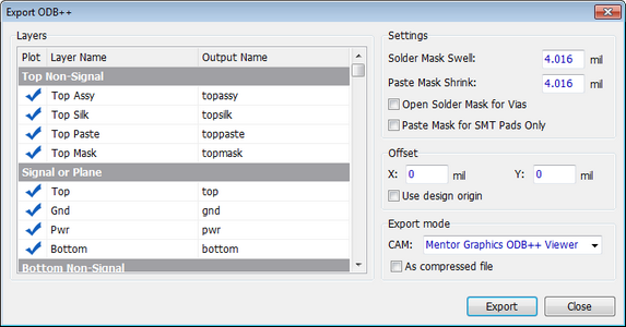
In the pop-up dialog box, the user can check or uncheck certain PCB layers for exporting, change default solder mask swell and paste mask parameters with respective fields and checkboxes, edit offset values and define the export mode. Default settings usually work for most cases. If As Compressed file item is checked, DipTrace will zip all ODB++ files into a single file for sending out to board manufacturer.
Press Export and specify the folder where to save the output file/s. You can preview ODB++ files with Mentor Graphics ODB++ Viewer.
3.2.7.7. IPC-2581
DipTrace supports IPC-2581 export, enabling its users to generate standardized, vendor-neutral files that encapsulate all the necessary information required for PCB fabrication, assembly, and testing. This export format is widely accepted in the industry, ensuring seamless communication with fabricators and enhancing the compatibility of your designs across different platforms.
To export in IPC-2581 format, navigate to File \ Export \ IPC-2581 from the main menu in the PCB Layout module.
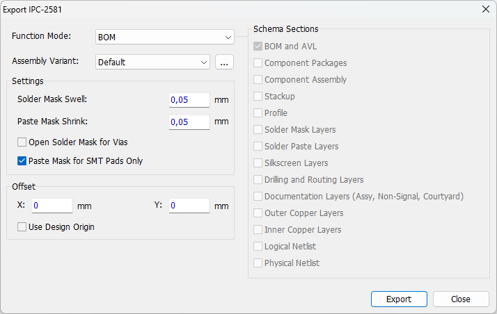
In the pop-up dialog select the desired Function Mode: BOM, STACKUP, FABRICATION, ASSEMBLY, TEST, STENCIL, DXF or a combination of thereof. Based on your selection, the relevant Schema Sections will be automatically chosen, with additional optional sections available for customization.
Select Assembly Variant, if applicable. To create a new one, press  button.
Adjust Solder Mask Swell and Paste Mask Shrink as needed. You can also opt to Open Solder Mask for Vias and/ or apply Paste Mask for SMT Pads Only.
Set the origin X and Y Offset, if necessary, or mark Use Design Origin.
Once all settings are configured, click Export and save the file in .xml format.
3.2.7.8. IPC-D-356A
DipTrace exports special-type coordinate netlist in the IPC-D-356A format, which PCB manufacturers use for bare board electric testing. Go to "File \ Export \ IPC-D-356A" from the main menu. In the pop-up dialog box, you can mirror the layout and change the offset values if you need. Offset is the shift of zero points from the bottom-left corner of the board. You can use current design origin by checking the Use Design Origin checkbox.
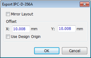
3.2.7.9. Mach 2/3 Drill
DipTrace exports a special G-code for drilling directly with Mach 2/3 software. Select "File \ Export \ Mach 2/3 Drill" from the main menu.
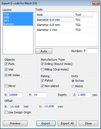
In the pop-up dialog box select the Objects which will be exported. After selecting the objects, fill out the list of Tools being used. You can manually assign tools by typing in the tool number in the Number: T field or press Auto to assign tools automatically.
Press Export All and DipTrace will determine all types of the holes automatically and export all necessary files for each type of the holes at a time. The user doesn't need to remember parameters of different via styles. Names of exported files consist of names of the top and bottom layer of the current hole type, the names are generated automatically (for example, "Through" or "Top-Inner1", etc.).
Offset is the shift of zero points from the bottom-left corner of the board. You can use current design origin while exporting the drill file by checking the Use Design Origin checkbox.
To mirror the layout, check the Mirror box. To preview the Mach drill file, select layers, and press the Preview button. Uncheck Plated and Non-Plated items to save plated and non-plated holes separately. Change the measurement units from inches to metric by checking the corresponding item.
Special parameters:
S – spindle speed, F – milling speed, Depth – milling depth.
If you want to save only the certain type of the holes, select all layers in order to export the through holes, for blind/buried holes select only the layer pair (top and bottom layer of the hole type). Use Ctrl or Shift keys to select several layers. Then press the Export button to save the file.
3.2.7.10. OrCAD TAP Drill
Export DipTrace layout to OrCAD TAP drill file. Go to "File \ Export \ OrCAD TAP Drill" from the main menu.
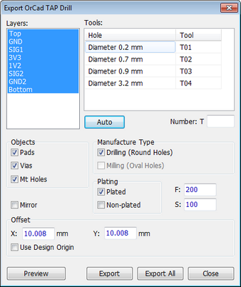
In the pop-up dialog box, select the Objects which will be exported. After selecting the objects, fill out the list of Tools being used. You can assign tools manually by typing in the tool number in the Number: T field or press Auto to assign tools automatically.
Press Export All and DipTrace will determine all types of the holes automatically and export all necessary files for each type of the holes at a time. The user doesn't need to remember parameters of different via styles. Names of exported files consist of names of the top and bottom layer of the current hole type, these names are generated automatically (for example, "Through" or "Top-Inner1", etc.).
Offset is the shift of zero points from the bottom-left corner of the board. You can use current design origin while exporting the drill file by checking the Use Design Origin checkbox.
To mirror the layout, check the Mirror box. To preview the Mach drill file, select layers, and press the Preview button. Uncheck Plated and Non-Plated items to save plated and non-plated holes separately. S – spindle speed, F – milling speed.
3.2.7.11. Bill of Materials
To create a bill of materials for the printed circuit board, select "File/ Export/ Bill of Materials" from the main menu. The following dialog box will pop up:
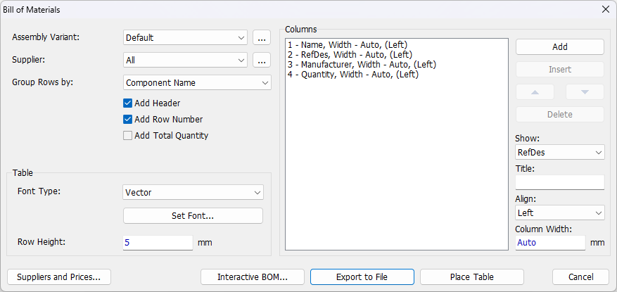
Select Assembly Variant from the drop-down or press  button to create and configure Assembly Variants. This option allows excluding some components from the BOM. Default variant represents the original layout and is not editable.
To create a new Assembly Variant press Add button, enter Assembly Variant Name in the pop-up and click OK. Remove blue check marks in the respective variant column to exclude components from the assembly. Use quick-selection buttons at the bottom of the window: All - to select all components, SMD - to select surface mount components only, Through-Hole - to select all through-hole components. Press Delete button to remove the currently active Assembly variant. Once the configuration of Assembly Variants is completed, press OK to save them.
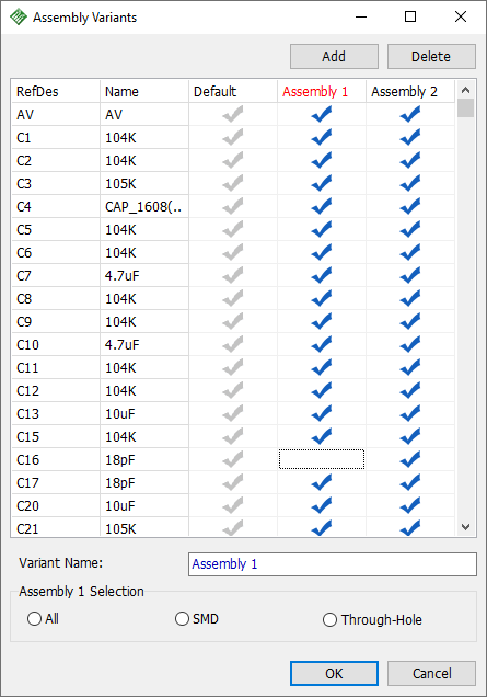
The rows of the BOM table can be grouped by components, component name, name and value/ pattern. Select the appropriate option from the "Group Rows by" drop-down list.
To show column headers, check the Add Header item.
Check Add Row Number to add the first column with row numbers ("1", "2", "3", etc.)
Check Add Total Quantity to add the last row with total quantity of components, parts, pins (depending on the row).
If you are going to place a BOM table directly in the project, use the Table section of the dialog to set font parameters and row height.
The columns of the BOM table can be defined as well.
To add a column, select component property from the Show drop-down list, set the column width, alignment, and press Add button.
To change parameters of the existing column, select it from the Columns list, and change the corresponding fields.
To insert a new column, select the position in the Columns list, and press the Insert button.
To delete a column, select it from the Columns list, and press the Delete button.
There are four ways to create a BOM:
1. Place a Table in the design area. To do that, press the Place Table button, and left-click on the design area, where you want the top left corner of the table to be located. An interactive table with all the components will be placed in the Top Assembly Layer.The components selected in the table are highlighted on the board. You can move the BOM table, like a regular table object. The table is updated automatically, so can keep editing your layout after placing the table - all subsequent changes will be included into the report.
Note that you can edit the table manually, however, auto-update mode will be disabled: left-click on any cell, a warning message will appear, click Yes - a Cell properties dialog will appear, allowing you to change cell parameters and its content.
2. Interactive BOM within PCB Layout - a pop-up table corresponding to the column and row settings will appear. The components selected in the table are highlighted on the board. Press Localize for DipTrace to center the component/-s from the selected row on the design area.
3. Export to File. The BOM files are available in 2 formats: Excel CSV and files with *.bom extension. When exporting to file, DipTrace will ask you to set a Column Divider and decide whether to use Quotation Marks for values or not. Please notice that you can add custom rows and columns to the BOM file in any spreadsheet editor.
4. Export HTML - this option provides for easy BOM sharing and revision outside the DipTrace environment. Save an HTML file and then open it in your browser.
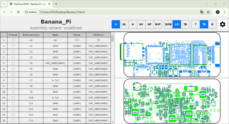
Use buttons in the top-right corner to configure BOM generation parameters, table and layout display mode.
U (Ungroup) - show each component of the circuit board in the BOM separately.
NL (Netlist) - generate a list of all the nets of the circuit.
N (Component Name) - group components in the BOM table by component name.
NV (Component Name and Value) - group components in the BOM table by component name and value.
NP (Component Name and Pattern) - group components in the BOM table by component name and pattern.
NVP (Component Name, Value and Pattern) - group components in the BOM table by component name, value and pattern.
BOM - show BOM table only.
LR - display BOM on the left and layout on the right.
TB - display BOM in the upper and layout in the lower part of the window.
T - show BOM and layout of the top side of the board only.
TB - show BOM and layout of both, top and bottom sides.
B - show BOM and layout of the bottom side of the board only.
3.2.7.12. Pick and Place
DipTrace allows the user to create Pick and Place Reports for printed circuit boards. To open Pick and Place Report dialog box, select "File \ Export \ Pick and Place" from the main menu in the DipTrace PCB Layout.
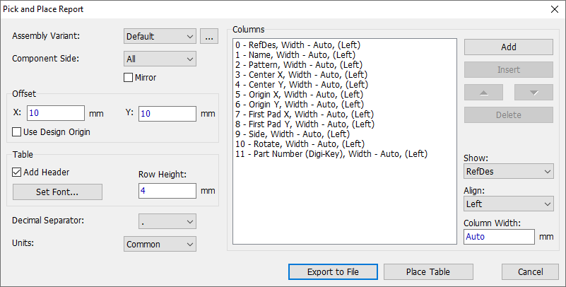
Using Pick and Place Report dialog box, you can create report files in Excel CSV and text formats or place an interactive table directly on the design area. The table is updated automatically, so can keep editing your layout after placing the table - all subsequent changes will be included into the report.
Select Assembly Variant from the drop-down or press button to create and configure Assembly Variants. Default variant represents the original layout and is not editable. Note that once configured, Assembly Variants can be accessed in both Pick and Place and BOM dialogs.
In Component Side drop-down, select, components from which side of the board you want to be exported.
Set Offset values for X and Y, if required. Or check Use design origin to set it as reference for components positioning.
Tick Add Header to generate a table with column headers. Press Set Font to change font parameters. Enter the required Row Height.
Decimal separator and units, different from those used in the project, can be set for Pick&Place report generation.
You can define columns of the report.
To add column, select component property from the Show drop-down list, set the column width, alignment, and press Add button.
To change parameters of an existing column, select it from the Columns list, and change the corresponding fields.
Show drop-down list contains the standard properties of the component (RefDes, Value, Name, etc.), data about component side, origin/ center/ first pad coordinates, package height and component rotation angle as well as parameters from the additional fields, if any (Unique Name, Part Number, etc.):
RefDes – component reference designator,
Value – component value,
Name – component name,
Pattern – component's pattern,
Package Height – the height of the component
Center X – X coordinate of the component center position relative to the component outline,
Center Y – Y coordinate of the component center position relative to the component outline,
Origin X – X coordinate of the component origin position,
Origin Y – Y coordinate of the component origin position,
First Pad X – X coordinate of the first pad terminal position
First Pad Y – Y coordinate of the first pad terminal position,
Side – component placement side (Top, Bottom),
Rotate – component rotation angle.
To change parameters of the existing column, select it in the Columns list, and change the corresponding fields.
To insert a new column, select position in the Columns list, and press Insert button.
To delete a column, select it in the Columns list, and press Delete button.
To place Pick and Place Report on the design area, press Place Table button, and left-click on the design area, where you want the top left corner of the table to be located. An interactive table with all the components will be placed in the Top Assembly Layer (the layer can be changed via Table Properties dialog to Bottom Assembly, Top or Bottom Silkscreen). The components from the row selected in the table are highlighted on the board. You can move the table, like a regular table object. The table is updated automatically, so can keep editing your layout after placing the table - all subsequent changes will be included into the report.
Note that you can edit the table manually, however, auto-update mode will be disabled: left-click on any cell, a warning message will appear, click Yes - a Cell properties dialog will appear, allowing you to change cell parameters and its content manually.
When exporting to file, DipTrace will ask you to set a Column Divider and decide whether to use Quotation Marks for values or not.
3.2.7.13. Solder Paste Dispensing
To export G-code for solder paste dispensing, navigate to File > Export > Solder Paste Dispensing. In the pop-up dialog, you'll find several options to customize the dispensing parameters.
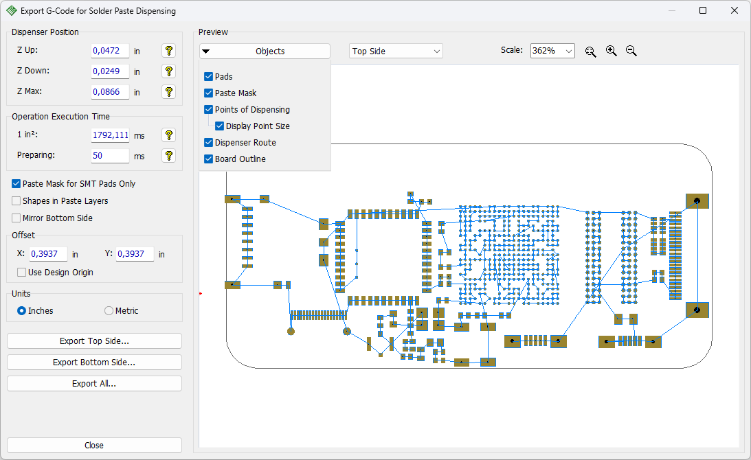
The Dispenser Position settings allow you to define the Z coordinates for various stages of the dispensing process:
Z Up sets the position while the tool moves to the next location;
Z Down defines the position for solder paste dispensing;
Z Max determines the Z position after dispensing, which is used to tear the solder paste material off the nozzle.
You can fine-tune the Operation Execution Time by setting the time required to fill 1 in? with solder paste and/or specify a delay before the tool starts filling each segment.
In the dialog, you can also select options for Paste Mask Application, such as applying it only to SMT Pads, including Shapes in Paste Layers, or using Mirror Bottom Side for a mirrored view.
For G-code generation, you can either set an Offset or choose to Use Design Origin as the reference point.
In the Preview section, you can choose which elements to display, such as Pads, Paste Mask, Points of Dispensing, Dispenser Route, and the Board Outline. You can also toggle between viewing the Top or Bottom side of the board. Additionally, you can adjust the preview scale either by entering a value manually or using the Zoom In and Zoom Out buttons.
Finally, you have the option to export the G-code for either the Top or Bottom side of the board individually or for both sides in a single file.
3.2.7.14. P-CAD ASCII
DipTrace allows the designer to export PCB layouts to P-CAD ASCII (*.pcb) format.
To export existing layout to P-CAD, select "File \ Export \ P-CAD ASCII" from the main menu, define filename, and save a file.
3.2.7.15. PADS ASCII 2005
DipTrace allows the user to export PCB layouts to PADS ASCII 2005 (*.asc) format.
To export existing layout to PADS select "File \ Export \ PADS PCB ASCII 2005" from the main menu, define filename, and save a file.
3.2.7.16. OrCAD Min Interchange
DipTrace allows the user to export PCB layout to OrCAD MIN Interchange (*.min) format.
To export existing layout to OrCAD, select "File \ Export \ OrCAD Min Interchange" from the main menu, define filename, and save a file.
3.2.7.17. Autorouter DSN
DipTrace allows for external automatic routing with highly efficient Electra and Specctra autorouters. Export a PCB to *.dsn format, route it with Electra or Specctra, and import results in *.ses format back to DipTrace.
Select "File \ Export \ Autorouter DSN" from the main menu and set filename in order to export design for routing.
It is important to keep the source *.dip file open while autorouting and importing the*.ses file. Import process can take couple seconds, depending on the project's complexity.
Do not make any changes to the design after you have exported DSN file and have not imported SES file yet.
3.2.7.18. 3D PCB model
DipTrace 3D Preview module allows the designer to export 3D model of the board to STEP (*.step) and VRML 2.0 formats (*.wrl) supported by most mechanical CAD software.
Open DipTrace 3D Preview & Export module (go to "Tools \ 3D Preview \ 3D Visualization" from the main menu), and press Export STEP button. Specify which objects to export with corresponding check boxes, and select model export mode in the pop-up dialog box. Then press OK, and specify filename and folder. Exporting Pad Holes can dramatically slow the process. We recommend exporting project as a solid body.
Notice that STEP models of circuit boards do not include copper traces on the board.
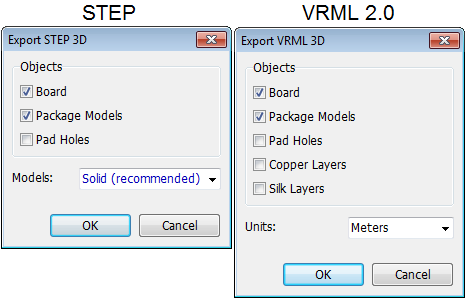
Press Export VRML button, select which objects to export with corresponding check boxes (Board, Package Models, Pad Holes, Copper Layers, Silk Layers), change measurement units if you need, then press OK, and specify filename and folder. Notice that if you export complex boards with a lot of holes, export process can be slow.
Circuit boards in the VRML format include all the copper traces, hence VRML format is better for demonstration.
3.2.7.19. Eagle XML
DipTrace allows a designer to export PCB layouts to Eagle XML (*.brd) format.
To export existing layout to Eagle, select "File \ Export \ Eagle board" from the main menu, define filename, and save the file.
3.2.7.20. Order PCB
DipTrace offers a special option for those who does not want to deal with Gerber files and PCB Houses.
You can order PCB manufacturing directly in the DipTrace software. No need to export Gerber files, just go to "File \ Order PCB" from the main menu. Follow the instructions (type in your address, the number of prototypes, the speed of production), and your project will be manufactured at our partner facility in California and delivered to your door (for contiguous US only).
3.2.8. Layout information
With Layout Information dialog box you can check the number of components, pins, nets, etc. and display holes by size, select "File \ Layout Information" from the main menu.
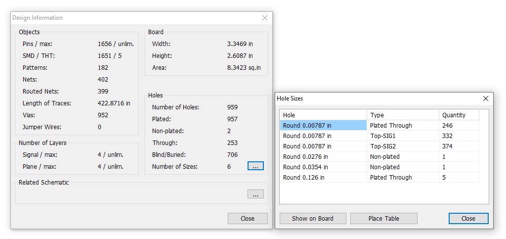
To display holes by size press button. Press Show on Board to highlight holes by size directly on the design area. You can place an automatically updating table on the design area and save it to CSV or text file (right-click on the table and select Save to File...).
3.2.9. Panelizing
DipTrace allows for panelizing of one or several different circuit boards on a single panel.
To replicate the current board on a panel, select "Tools \ Panelizing" from the main menu or press  button on the Standard toolbar. The following dialog box will pop-up.
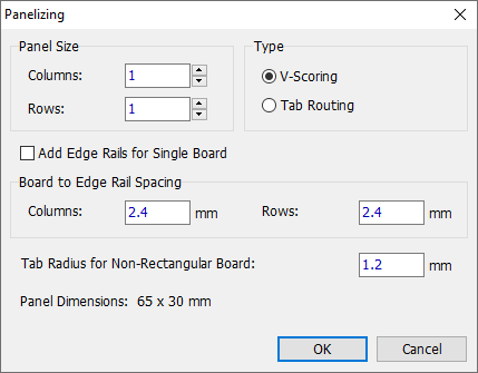
Select V-scoring or Tab Routing panelization type.
Note that the Panelizing tool also allows adding edge rails to a single PCB. Mark Add Edge for Single Board and set the width of the rails.
V-scoring
Set the number of Columns and/ or Rows, in the Panel Size section.
Check Add Edge Rails checkbox to add rails of defined size on the sides of the panel.
Enter Board to Board Spacing for a rectangular board or Board to Board and Board to Edge Rail Spacing values for non-rectangular board, taking into account your manufacturer's requirements for the V-groove size.
V-scoring is recommended for boards with regular shape, however, it can be combined with routing and used for irregular boards. If it's the case, set Tab Radius for Non-Rectangular Board. Make sure that 2xR value does not exceed Board to Board spacing.
Panel Dimensions - shows the calculated size of the panel based on the user-defined panelization parameters.
Tab Routing
Set the number of Columns and/ or Rows, in the Panel Size section.
Check Add Edge Rails checkbox to add rails of defined size on the sides of the panel.
Keep Material at Empty Areas option allows maintaining dielectric in some areas of the panel, creating a more rigid panel.
To add Tabs between edge rails select the required option from the drop-down (Horizontal, Vertical).
Enter Board to Board and Board to Edge Rail Spacing values, taking into account manufacturer's requirements for the selected panelizing type.
Note that if Tab routing option is used, this value correlates with the Tab Corner Radius.
Define Tabs and Mouse Bites parameters based on your manufacturer's requirements.
To create Tabs without mousebites, set 0 as Hole Diameter.
Use negative Inset value to displace mousebites towards tabs.
Tab Count for a Single Board - the number of Tabs on the horizontal and vertical sides of the board is calculated based on the Board Size and previously defined Tab Step. The calculated number is shown as a tip on the right. However, you can set Tab Step to 0 and customize the number of tabs by entering the required values in the Horizontal and Vertical cells.
Panel Dimensions - shows the calculated size of the panel based on the user-defined panelization parameters.
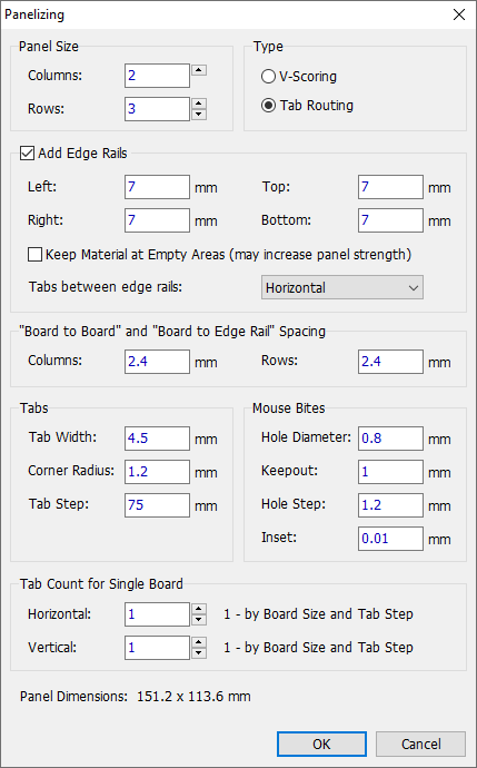
Patterns, shapes, copper pours, and tables can be excluded from panelizing. Right-click on selected object/s on the design area, and check Do Not Panelize in the submenu. Item is visible only if Panelizing feature is active.
How to panelize different projects on a single board
– Open the first PCB, right-click on its board outline, and select Convert to Shape from the submenu. Then press Ctrl+A hotkeys to select all objects and Ctrl+C or "Edit \ Copy" from the main menu to copy them;
– Open the second PCB in another DipTrace PCB Layout instance, check "Edit \ Keep RefDes while Pasting" from the main menu to keep all reference designators of the project you are about to paste, right-click on the design area where you want to insert another project, and select Paste from the submenu.
3.3. Working with libraries
3.3.1. Review
In DipTrace a typical electronic component consists of a schematic symbol, PCB footprint (pattern) and possibly a 3D model. All these entities represent a component on various design stages. The PCB Layout module works with component patterns, which represent real footprints of electronic components on the printed circuit board.
Refer to Component Editor Help and Pattern Editor Help for more details about designing components, footprints, and libraries.
Place Component panel is on the left side of the screen. It has all necessary tools for placing components as well as managing libraries and library groups in all DipTrace modules.
Libraries are organized to library groups for convenience.
There are five library groups available by default:
1) Components (all standard libraries, user can not edit this library group);
2) Patterns (all standard pattern libraries separately from the schematic symbols, the user can not edit this library group);
3) User Components (designer adds/deletes component libraries to/from this group);
4) User Patterns (designer adds/deletes pattern libraries to/from this group);
5) Project Libraries (auto-generated library with all components from a current circuit).
Library Setup dialog box allows the user to add libraries from the separate files into DipTrace system, create new and edit existing library groups. Changes in the library structure made in the PCB Layout immediately affect the libraries in the Schematic and other software modules. PCB Layout works with both component and pattern libraries.
It is possible to search components in all libraries by applying search filters. Select "Objects \ Find Component" from the main menu or press  button on the Place Component panel to set up and apply the filters.
3.3.2. Library groups
Library groups are very easy means of organizing libraries. There are five default library groups: Components, Patterns, User Components, User Patterns and Project Libraries (auto-generated library group for storing all components of active layout in the Design Cache library).
Press  to change active library group or open the Library Setup dialog box to create and edit library groups and connect separate libraries from the files.
Press  to change move/copy/delete pattern libraries between the library groups.
3.3.3. Library setup
Place Component panel allows the user to find and place components and patterns. Select the library group, then select library from the list, and select component from the list right below to place it on the design area.
Library Setup
Go to "Library \ Library Setup" from the main menu or press and select Library Setup from the submenu. In the pop-up dialog box, the user can create library groups and add/delete libraries to/from the groups. The Library Setup panel is the same as in Schematic and allows the user to edit not only component library groups but pattern library groups as well.
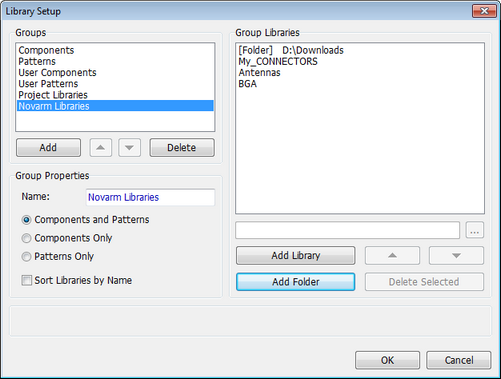
Press Add to create new library group, type in its name into the field below, and select the group type, depending on what libraries you are going to store in the group:
Components Only type allows for adding only component libraries (files with *.eli extension) to the group;
Patterns Only type allows for adding only pattern libraries (files with *.lib extension);
Components and Patterns type allows for adding both library files into current library group.
Select library group from the list, and press Add Library or Add Folder buttons to add libraries from the files to the library group.
The user can not edit the standard library groups: Components and Patterns.
3.3.4. Search patterns
Search filters help to find components by various parameters. Select "Objects \ Find Component" from the main menu or press button on the Place Component panel. Select a search area (where to search for components), type in the name, and press Apply Filter. Press + or - buttons to add/delete new filters, which allow for finding components by RefDes, Value, Manufacturer, Pattern, Datasheet or Additional Fields.
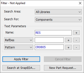
Press Search at SnapEDA button to open SnapEDA dialog and look up the components based on the entered parameters in SNapEDA libraries directly from within DipTrace.
Press New Part Request to be directed to the 24-Hour Component Design Service, where you can place an order for the required component design.
3.3.5. Search at SnapEDA
To look for the required components in SnapEDA libraries, go to "Objects \ Search Parts at SnapMagic". In the pop-up, register or log-in, if necessary, enter data in the Search field and press button.
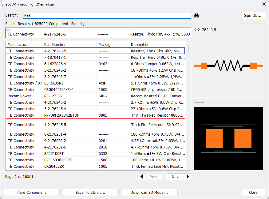
Select a component from the search results, its symbol and pattern will appear in the preview field, if available.
Press Place Component button to place the pattern directly on the design area.
Save to Library button allows adding the component to the existing user library or to a newly-created one.
Download 3D Model button gets active, if a 3D model is available for the selected component. Press it to download the .step file to your computer. The model will be automatically attached to the respective pattern.
3.3.6. Save components as a library
DipTrace PCB Layout module allows the designer to save selected patterns of the current circuit board as a new pattern library or add them to the existing one. Select patterns on the design area, right-click one of them, and choose Save To Library from the submenu.
Design Cache (auto-generated library with all patterns of the design) can be saved as well – select Design Cache library, press , then select Save Design Cache as Library from the submenu.
3.4. View functions
3.4.1. Toolbars
PCB Layout has eight main toolbars:
To show/hide the toolbars and panels, select "View \ Toolbars" from the main menu and then check corresponding items (the majority of toolbars have hotkeys for displaying/hiding them). Design area size changes automatically when you change the toolbar layout. Toolbars configuration is saved when you close DipTrace.
3.4.2. Scaling/Panning
There are several ways to change the scale of the design area:
1. The mouse wheel – you can decrease or increase scale within very wide limits.
2. The drop-down list on the Standard toolbar (from 25% to 800%).
3. "View \ Scale" from the main menu. It is possible to select from 25% to 800%, zoom in, zoom out or specify custom scale.
4. Plus sign (+) and minus sign (-) default hotkeys to zoom IN/OUT.
5. "Zoom window" or "Zoom Extents" tools on the Standard toolbar for mouse-defined zone zoom.
The current scale is always displayed in the drop-down list on the Standard toolbar.
Panning the design area is possible with the right mouse button (hold down and move) or by arrow keys when you create wire, shape or another object.
3.4.3. Layers/Objects/Properties
Show/Hide design layers in the Layers tab on the right side of the screen (Design Manager panel). Here you can change layer color and name.
Objects tab allows the user to show/hide objects by type or disable object highlighting selection (drop-down list).
When an object or tool is selected, its main parameters are displayed in the Properties tab.
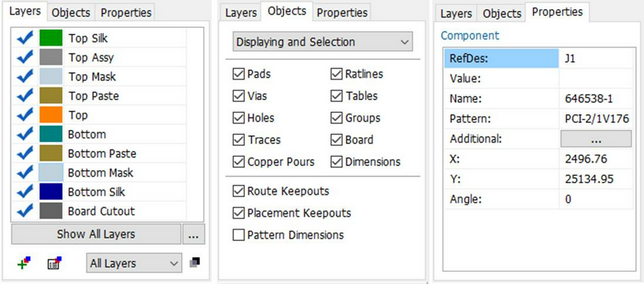
You can also show/hide different objects in the "View \ Objects" main menu item.
3.4.4. Ratlines
Sometimes the designer needs to hide ratlines for selected nets, optimize ratlines structure or show/hide ratlines only for current net or component. All these opportunities are available in the "View \ Ratlines" main menu item.
Optimization feature minimizes the length of all ratlines (blue lines), select "View \ Ratlines \ Optimize" or just press F12 hotkeys to optimize ratlines.
To show/hide ratlines for the net, right-click on the pad or any trace that belongs to this net, and select Hide Net Connections from the submenu. You can show ratlines for all nets any time, just select "View \ Ratlines \ Display All" from the main menu.
The best option is to hide ratlines of all other nets, except the one being routed manually. Check "View \ Ratlines \ Routed Net Only" item in the main menu. This option is duplicated in Routing Setup dialog box (the Settings tab).
When you move a component, its ratlines are shown. All other ratlines of the design are hidden by default. Select "View \ Ratlines \ Moved Component Only" option in the main menu to customize this feature.
3.4.5. Net highlight and color
In DipTrace PCB Layout, the color of traces on the design area by default depends on the layer color, but the software allows for setting custom colors. Right-click on a copper trace on the design area, select Trace Color from the submenu, and select Custom. In the pop-up dialog box, you can set any color to the trace, and press OK. All traces, pads, copper pours, and shapes that belong to this net will change their color.
You can permanently highlight any of the traces with a dotted contour line regardless of its color. Right-click on the trace, and select Highlight Net from the submenu.
3.4.6. Component markings
To set up default component marking options, select "View \ Component Markings" from the main menu in the DipTrace PCB Layout. In the pop-up dialog it is possible to adjust settings to show RefDes, Value, Name, Pattern, Manufacturer, Datasheet or any additional field of components. Align markings by the center, top, bottom, left, right, top-right corner of the pattern or automatically (DipTrace will calculate the best position). You can define the settings for the Silk Screen and Assembly Layer individually.
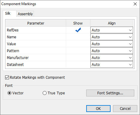
Uncheck Rotate Markings with Component if you want text fields to maintain their position when the component is rotated.
Here you can also change type (Vector or True Type). We strongly recommend using the Vector font for English characters and TrueType font type for Unicode symbols. Press Font Settings button to open Font dialog, where you can set the font size, select the Line Width (Thin, Normal, Bold or Custom), and also define the Text Width:
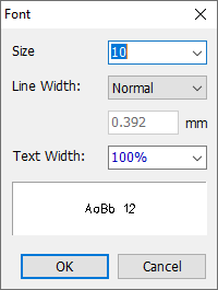
Those settings apply to all components on the design area, except those with custom marking settings.
To set up custom component marking settings, right-click on the component, and select Properties from the submenu, then select the Markings tab in the pop-up dialog box and make the necessary changes.
To move component marking, select "View \ Move Component Texts" from the main menu or press F10 default hotkey. Select marking and change its position by dragging with the mouse. To rotate marking by 90 degrees in this mode, press R or Space (when the Move Component Texts tool is active).
3.4.7. Pad/ Trace Markings
Pad Markings can be displayed as Pad Numbers, Net Names, or both. To select your preferred option, go to View/ Pad Markings and choose the desired setting.
To enable Net Marking for DipTrace to show net names on the traces, go to View/ Net Markings and mark this option.
3.4.8. Assembly Layer
You can automatically add pattern drawings, pads, pattern silk, borders, texts (RefDes, Value, etc.) and board outline to the Assembly layer. Select "View \ Add to Assembly" from the main menu to add new objects to the Assembly layers.
You can also add custom non-signal layers on any side of the board.
3.4.9. Jumper wires
DipTrace allows the user to route boards with jumper wires (use the right-click submenu or J (by default) hotkey while in the routing mode). DipTrace creates vias free from mask in the start and end points of the jumper wire trace segment.
You can show jumpers in silk, assembly, signal layer or do not show them at all, just go to "View \ Jumper Wires" from the main menu to set up the visibility.
3.4.10. Pad numbers
In DipTrace PCB Layout you can display pad numbers for components (footprints) and change their font.
To display pad numbers, select " View \ Pad Numbers \ Show" from the main menu.
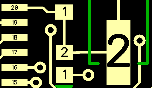
To change font size for pad numbers, go to "View \ Pad Numbers \ Font". Auto-sizing is a default parameter, it scales the font size depending on the pad size.
3.4.11. Grid
DipTrace allows the user to create and edit objects freely or strictly according to the grid on the design area. If the grid is visible and Snap to Grid option is enabled, patterns and other objects are aligned on the grid with different key points: first pad, traces, shapes.
To show/hide the grid, select "View \ Grid" from the main menu or press F11 hotkey (by default).
Select "View \ Snap to Grid" from the main menu, or press Alt+F11 hotkey (by default) to activate/deactivate snap to grid, when the grid is on.
If Snap to Grid option is disabled, layout objects are no longer snapped to the grid, but you can leave the grid visible.
When Snap to Grid option is disabled for the entire project, you can choose to snap to grid individual elements of your pattern (pad, shape, text, image, etc.) by selecting Snap to Grid item from the right-click submenu of those elements, when the grid is on.
To open grid size submenu, select "View \ Grid Size" from the main menu. Here you can select the grid size from the list of available sizes or specify custom grid size. Use drop-down list on the Standard toolbar or just press Ctrl + Plus sign, Ctrl + Minus sign (by default) to quickly change the grid size.
To change the list of available grid sizes, select "View \ Customize Grid" from the main menu.
To configure the precision and set the minimum grid size value, select Precision.. item in the View submenu and define the respective parameters in the pop-up dialogue-box.
3.4.12. Origin
Design origin is a customizable point on the design area. The user can change its position at any moment while creating or editing the layout.
To show/hide the origin, select "View \ Display Origin" from the main menu or press F1 hotkey (by default).
Change the origin's position with the mouse pointer or by coordinates (incrementally from the existing origin). To define origin with the mouse, select "View \ Define Origin \ By Mouse Pointer" from the main menu or press button on the Elements toolbar, then define a new origin with a left-click on the design area. To change origin by coordinates, select "View \ Define Origin \ By Coordinates" from the main menu.
To return origin to default position (center of the sheet) select "View \ Define Origin \ Default Position."
3.4.13. Titles
To show/hide titles, select "View \ Display Titles" from the main menu.
Specify sheet size and orientation, border margins, zones and title blocks in the Sheet and Titles Setup dialog box (select "View \ Sheet and Titles Setup" from the main menu or press  button on the Standard toolbar). To create custom title block, press the Title Block Editor button in the Sheet and Titles Setup dialog box.
To change text, font and alignment of the title block field, move the mouse cursor to the corresponding field, and left-click it.
To show/hide the sheet border on the design area, select "View \ Display Sheet" from the main menu.
It is possible to change titles and sheet display mode from the Sheet and Titles Setup dialog box.
3.4.14. Mirror design
To mirror layout horizontally, select "View \ Mirror" from the main menu. This does not affect the layout when exporting the layout for manufacturing.
For printing purposes, mirror the layout in the Print Preview dialog box.
3.4.15. Measurement units
Possible measurement units: mm, mils, and inches.
To change current units, select "View \ Units" from the main menu or use Shift+U keyboard combination.
To adjust the precision level by units, open the Precision dialogue-box via View\ Precision menu and specify the number of decimal places for all the values used in the current project.
Please note that high precision rates are used only at designing stage. When the project is saved into a file, precision up to 0.001 mil is applied.
3.4.16. Line width
DipTrace allows the user to change line width of the pattern silkscreen, component outline, courtyard, tables, titles and board outline as well as to set this value for all other layers.
To open line width dialog box, select "View/ Line Width" from the main menu.
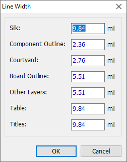
The width of the lines of individual shapes can be customized in Shape Properties dialogue accessed by selecting Properties from shape right-click submenu.
3.4.17. Graphics mode
Schematics and PCB Layout modules support Direct3D and OpenGL graphics modes to increase the drawing speed comparing to Windows GDI mode. You can select the graphics mode from the "View \ Graphics Mode" main menu item.
1. Direct3D is the fastest mode for typical Windows PC and we recommend to use this mode for most workstations. However, this mode depends on hardware, drivers, and their versions, therefore some issues are possible, especially with new/buggy or outdated OS/drivers.
2. OpenGL usually works a bit slower than Direct3D but is less dependent on hardware/drivers. OpenGL is the best choice for high-end engineering stations with professional OpenGL graphic adapters. You can try both modes with very complex projects and choose the best for you.
3. Windows GDI is an alternative mode for those who is not satisfied with Direct3D and OpenGL. Windows GDI is much slower but doesn't depend on drivers/hardware/OS. Good for small and medium-sized projects.
3.4.18. Precision
Precision
DipTrace allows adjusting the precision rate for project values and the grid.
Select View/ Precision… to open the following dialogue-box:
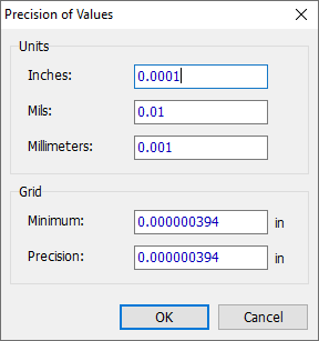
Configure the precision level by defining the number of decimal places (up to ten) for all the values used in the project by units.
You can also set the minimum grid size and grid precision for the current units. Those values are converted, when measurement units are changed.
Please note that high precision rates are used only at designing stage. When the project is saved into a file, precision up to 0.001 mil is applied.
3.4.19. Colors
Edit color template of the design area and all its elements. Select "View \ Colors" from the main menu.
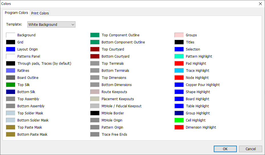
Three color templates are available: White Background, Black Background, and User Defined. You can select a template from the Template box. The white background is used by default, but for most users, black background seems to be more eye-friendly.
To define the color of specific elements, click on the color rectangle next to the object name, and select a new color in the pop-up dialog box. The custom color scheme is automatically saved as "User Defined" template.
In order to change the print colors, select the corresponding tab in the Colors dialog box. White background template is used by default.
Notice that colors you use in the PCB Layout module are applied to Pattern Editor, same for Schematic and Component Editor which share one color scheme as well.
3.5. Objects
3.5.1. Component
3.5.1.1. Review
A regular component consists of schematic symbol and pattern with attached 3D model. The pattern is the component footprint on the printed circuit board.
A component pattern contains pads, shapes, mounting holes and fiducials. Pattern Editor is the tool to create and edit patterns.
There are 9 different types of patterns:
1. Empty – does not depend on pattern parameters. Pads do not form any shape.
2. Circle – contains pads which form a circle. It depends on the number of pads and pad-to-pad spacing.
3. Lines – contains certain number of pad lines. It depends on four parameters: number of lines, number of pads, pad-to-pad spacing, and line-to-line spacing.
4. Square – contains four pad lines which form a square. It depends on three parameters: number of pads, pad-to-pad spacing, and line-to-line spacing.
5. Matrix – contains pads which form the matrix. It depends on the number of columns, number of rows, column spacing and row spacing.
6. Rectangle – four pad lines form a rectangle. It depends on 5 parameters: horizontal pads, vertical pads, pad spacing, width, and height.
7. Zig-Zag – pads form a zig-zag. It depends on 3 parameters: number of pads, pad-to-pad spacing, and line-to-line spacing.
8. Pad – pattern with only one pad. It can be created in the Pattern Editor and PCB Layout using the Place Pad tool.
9. Mounting Hole – contains only one mounting hole. It can be created in the Pattern Editor and PCB Layout using the Place Mounting Hole tool.
10. Fiducial – contains only one fiducial. It can be created in the Pattern Editor and PCB Layout using the Place Fiducial tool.
3.5.1.2. Place component
Patterns can be placed quickly from the Component Placement panel or using the Place Component dialog box ("Objects/ Place Component" from the main menu or with  button on the Elements toolbar).
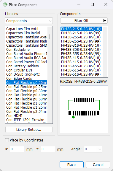
In the pop-up dialog box select the library group, then select library, and place component manually or by coordinates.
You can easily access the Library Setup and search filters. Pattern preview is also available.
Use R or Space bar to rotate component before placement. You can drag and drop the component to change its location; guidelines will appear while moving it to help you align it with other components.
3.5.1.3. Replace Component
Patterns can be easily replaced using the Replace Component dialog box. To open it, right-click on the component/s you want to substitute and select Replace Component from the submenu. In the pop-up dialog box, select the library group, then the library, and the component. You can use automatic search filters to narrow down your search results as well as redirect the search to SnapEDA libraries.
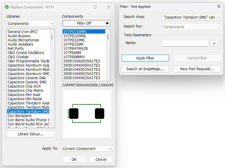
The substitution can be applied to the Current Component, Similar Name Components or Selected Components.
Note that when replacing a component with another one, DipTrace will maintain the existing connections and routing.
3.5.1.4. Create pattern
The special feature of DipTrace PCB Layout allows the users to create patterns directly in the PCB Layout module without using the Pattern Editor.
Place pads and shapes, select them, right-click on one of selected objects, and choose Group into Component from the submenu. All selected objects will be grouped into a single component pattern.
Ungroup pattern
To convert any component to the set of pads and shapes, right-click on the component, and select Ungroup Component from the submenu. Ungroup feature breaks Schematic-to-PCB links of components and component RefDes, therefore we do not recommend to use this feature if you have created PCB from Schematic and plan to update it in future.
3.5.1.5. Properties
Right-click on the component pattern, and select Properties from the submenu to open the Component Properties dialog box in the PCB Layout.
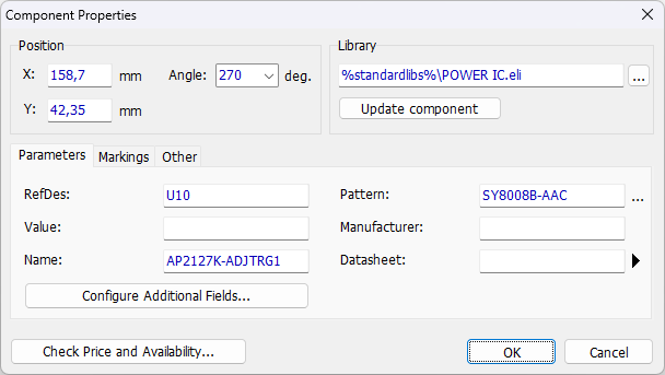
Here you can adjust component position by setting its X and Y coordinates and rotation angle.
Component can be updated from the selected library. Press button to browse for the required library file. Press Update Component button to apply changes.
This dialog box allows for changing the RefDes, Name, Value, Pattern name, manufacturer, datasheet, and additional fields of the component on the Parameters tab, variable parameters in the Variables tab (visible only for components with variable parameters, change pads and dimensions based on the pattern type).
Press Configure Additional Fields button to add more descriptive fields.
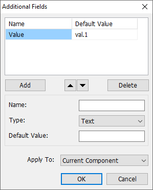
Type-in the Name of the new additional field, select its type (Text or Link) and set Default Value. Press Add button. Use arrows to change the position of the selected field in the list. To delete a custom field, select it and press Delete button.
New fields can be added to the Current Component, Selected Components, Similar Name Components, components with Similar Set of Fields or All Components of the layout.
In the Markings tab you can choose to show/hide certain marking/-s (RefDes, Value, Name, etc.) or apply Common (default) display settings (defined in the "View \ Component Markings" main menu item) to a given component. Markings display parameters for the selected component can be defined individually for the Silk Screen and Assembly layers.
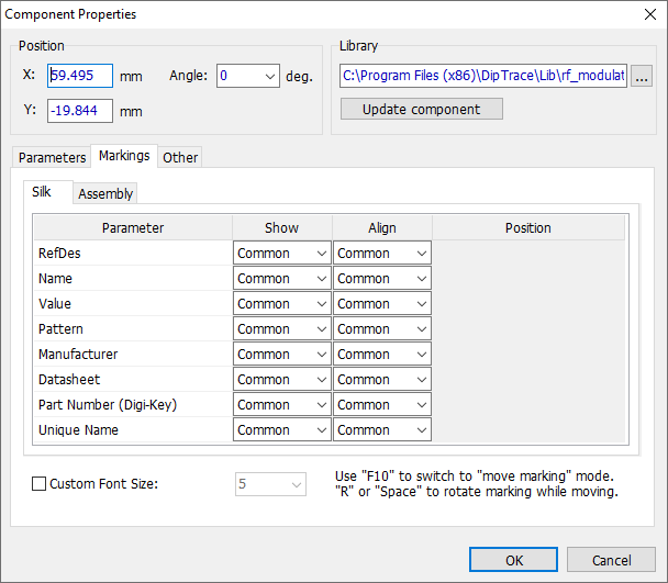
To define marking alignment settings, select the necessary option from the drop-down in Align column. The markings can be adjusted by the top, bottom, left, right, the center or corner of the component. You can also apply Common or Auto settings. In the first case, the software will use default parameters set for the entire project (View/ Component Markings). If Auto mode is selected, DipTrace will automatically select the best location for the markings. There is one more Aligning option - Position. Use it for precise Markings placement. Once selected, an active line appears in Position column. Press button to select the location of Markings anchor point, set its coordinates and rotation angle.
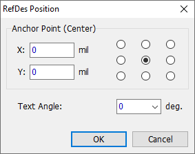
Font size of the displayed Markings can also be customized in this tab - tick Custom Font Size and select required size from the drop-down.
Placement tab allows the user to define a custom clearance for the selected component. This clearance will be used for component arrangement and auto-placement features.
Press Check Price and Availability to search for the selected component on Mouser website or in our Supplier Database.
3.5.1.6. RefDes renumbering
Renumber the reference designators from the top-left to the bottom-right for the convenience of exploring the layout. Select "Tools \ RefDes Renumbering" from the main menu or right-click on the component, and select RefDes Renumbering from the submenu.
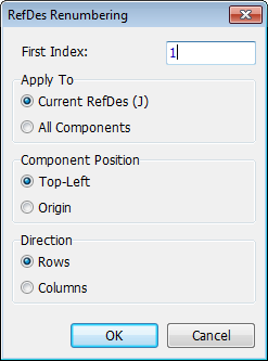
Apply renumbering to all reference designators of the layout or only to current RefDes (option is available only if renumbering launched from the component submenu).
Renumbering is possible by rows or by columns:
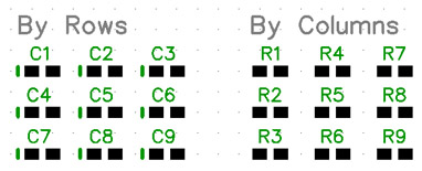
Component position in the renumbering table can be determined by the top-left corner or by the pattern origin point.
3.5.1.7. Standard Pad properties
Set pad properties for entire component or separately for each pad.
To change component pad properties, right-click on the component, and select Standard Pad Properties.
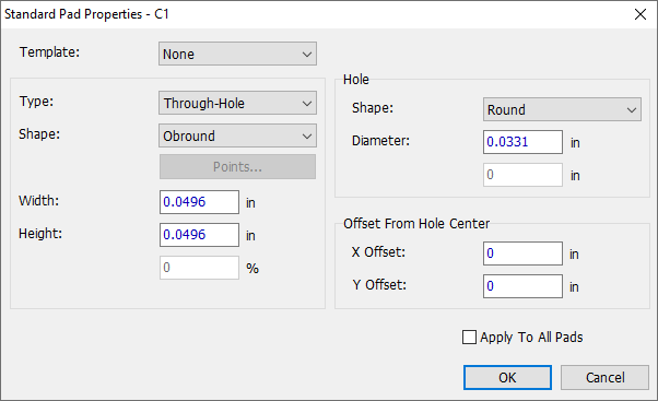
In the pop-up dialog box set the pad type (through-hole or surface), pad shape (ellipse, obround, rectangle, polygon or D-shape), pad width and height, hole shape (round or obround) and hole diameter or dimensions. For through-hole pads you can also define X/Y offset of the pad shape from the hole center.To apply changes to all the pads of the selected component, check Apply to All Pads item, otherwise, changes will be applied to default pads only (pads where Use Pattern's Standard Pad Properties box is checked in the Properties dialog of individual pads).
To open the Pad Properties dialog box for the selected pad, right-click on the pad, and choose Pad Properties. In the pop-up dialog box uncheck Use Pattern's Standard Pad Properties item, and additional fields will appear.
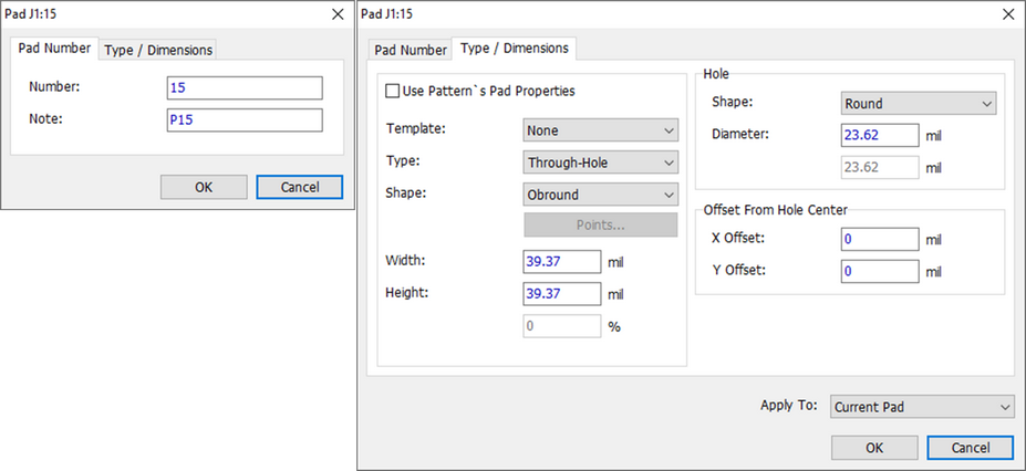
Set the number and note for the pad and keep other settings. Changing custom pad settings is possible only if Use Pattern's Standard Pad Properties item is unchecked. Changes can be applied to the current pad, all similar pads of the design, or similar pads of selected pattern.
If you select polygonal pad shape, you can set points of the polygon, just press the Points button.
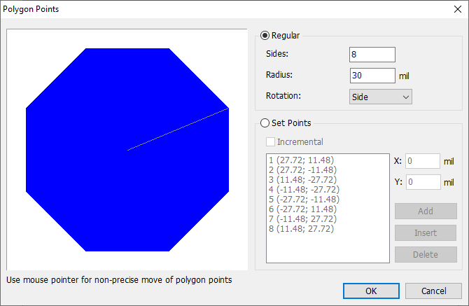
In the pop-up dialog box set the polygon type: regular or by points.
To define a regular polygon, specify the number of sides and rotation align.
There are the following functions to edit polygon points:
– add a new point, enter coordinates to X and Y fields, and press Add button;
– delete points, select the points, and press Delete button;
– change point coordinates, select point, and specify new coordinates;
– insert a new point, select correct position, and press Insert button.
Edit points visually – drag & drop in the preview field.
Notice that you can hide pad shape in any signal/plane layer. Right-click on the pad, and select Hide Pad Ring in Layer. Blind/buried pads are possible. Right-click on the pad to display its submenu, and select Pad Layers from the submenu.
3.5.1.8. Pad thermal settings
Pads can have custom thermal settings (different from the copper pour properties). Right-click on the pad, and choose Thermal Settings from the submenu.
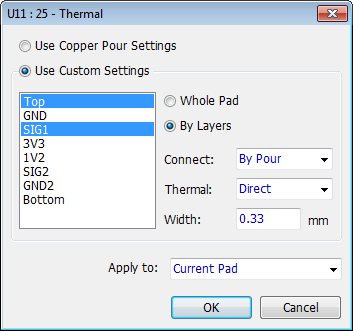
In the pop-up dialog box, by default, the Use Copper Pour Settings box is checked. This means that common copper pour settings apply to this pad.
Check Use Custom Settings, and define custom thermal settings for the Whole Pad or By Layers.
Other fields:
Connect means that you can remove or add a thermal connection for the pad regardless of the net in copper pour settings.
Thermal is a thermal connection type applied.
Width is a spoke width used for non-direct connection types.
Apply settings only to the current pad, to all similar pads, or to selected component.
Note that if a pad or component is rotated, pad to copper pour thermals are also rotated to the same angle.
3.5.1.9. Pad teardrops
Teardrop parameters for trace to pad/via/ trace junctions of the selected objects or all existing junctions of the circuit board are defined in the Add/ Change Teardrops dialog launched by selecting Teardrops item from the Route menu. However, those parameters can be set for individual pads as well.
Right-click on a pad and select Teardrops item from the submenu. Tick the necessary pad type checkbox - Through-Hole Pads and Vias or SMD Pads (or both) - and define the teardrop Length and width in the Connection area as a percentage of the pad (for through-hole) or trace (for SMD) size.
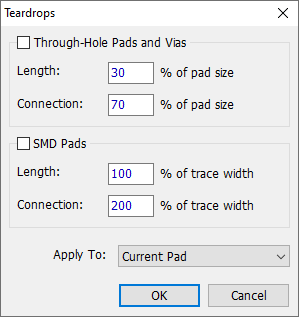
Note that connection width is limited by the pad width.
Apply the settings to the Current Pad only, or to the Selected Objects - in this case teardrop junctions with the defined parameters will be created for all pads of the selected component/-s.
Note that teardrop settings of individual pads have priority over those defined for the net.
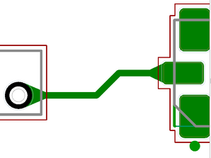
3.5.1.10. Pad mask and paste
Default solder mask and paste settings for all pads on the circuit board are defined in the Gerber export dialog box. However, pads can have custom properties in the solder mask and paste layers. Right-click on the pad, and select Mask / Paste Settings to change custom pad solder mask/paste properties.
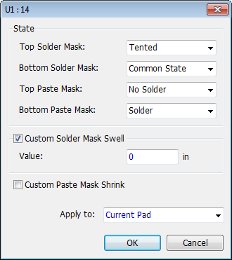
Select the state of the top/bottom solder mask/paste of the pad, using respective drop-down lists in the State section of the dialog box.
Common state – apply default solder mask and solder paste parameters to the pad;
Open – pad not covered with solder mask regardless of the default parameters;
Tented – pad covered with solder mask regardless of the default parameters;
By Paste Mask – solder mask will match Paste Mask;
Solder – apply solder paste to the pad regardless of the default parameters;
No Solder – do not apply solder paste to the pad regardless of the default parameters.
Segments – a useful option for big pads, which allows splitting paste into segments instead of filling the entire pad area. With this option selected you can define fill percent, min. segment side, min.segment gap and nominal edge gap for the paste mask segments.
If you need custom solder mask swell and paste mask shrink settings for the pad/s, check the respective check boxes, and enter custom values (negative numbers are supported).
Changes can be applied to the current pad, to all similar pads, or pads of the selected components.
3.5.2. Net
3.5.2.1. Review
Net is a logic connection between two or more component pads. Thin blue ratlines show unrouted nets; traces show the routed ones. Ratlines are always blue, while the trace color depends on the layer color (it is specified in the signal layers dialog box).Nets can also have the custom color (set in the right-click submenu).
You can create ratlines directly in the PCB Layout or open schematic file (*.dch) with the net structure built in the DipTrace Schematic. Create traces manually or let the autorouter do it.
The software does not allow for nets outside net classes. Net class parameters (trace width, clearance, min/max length, etc.) apply to net automatically. Proceed to the Net Classes dialog box to change net class parameters. Editing the Default net class is also possible in the Routing Setup dialog box.
Net consists of one or several traces. A trace is a part of the net between two pads. A segment is a part of the trace between two nodes.
Trace segments can have different width and can be placed on different signal layers. When two adjacent segments of one trace are placed on different layers, vias appear automatically to ensure reliable electric connection.
3.5.2.2. Net classes
Typical circuit boards usually have several net classes with different properties. All nets in DipTrace belong to net classes. Net class determines the following properties of the net: type (regular net or differential pair), basic trace width, basic and detailed clearance (object-to-object), length matching rules, possible via styles, auto-routing settings (priority, max. number of vias in one net, max. incorrect way, routing layers, and phase/length/neck settings for differential pairs). To add/edit net classes and move nets from one net class to another, select "Route \ Net Classes" from the main menu. The following dialog box appears:
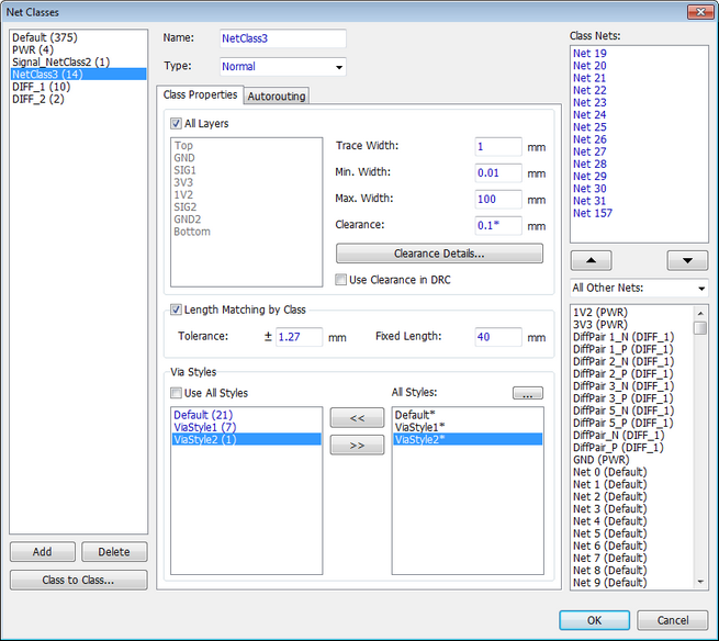
Here you can add/delete net classes and edit their properties. You can not delete a net class if at least one net still belongs to it. Nets should be moved to another net class prior to deleting. Use lists on the right side of the dialog box to move nets (the upper list displays the nets that belong to the class and the lower list shows all other nets or nets sorted by net classes).
Check Length Matching by Class if you want to match the lengths of all nets in the class and automatically create a DRC rule to verify traces.
All nets are automatically assigned to the Default net class. You can not delete this class, but you can edit its properties.
You can configure the trace width and clearances on the per-layer basis (uncheck All Layers box and configure settings for each layer individually).
The Class-to-Class button allows the designer to configure class-to-class clearances.
Notice that DRC verifies the circuit board against these values because class-to-class clearances have higher priority than regular net class clearances.
3.5.2.3. Create net
There are several ways to add ratlines (create new nets) in the PCB Layout:
1. To connect two pads with the mouse, select "Objects \ Place Ratline" from the main menu or press button on the Objects toolbar. Then left-click on the first pad, and move the mouse to the second pad. Left-click the second pad, and connection line appears (new net is created). Right-click if you want to cancel the connection while creating it and switch to the Default mode. Connect as many pads as needed.
2. To connect pad to existing net, right-click on the pad, and choose "Add to Net \ Select from List" from the submenu. Then select net, and click OK. Ratline appears heading from the current pad to the nearest pad of the specified net.
Connect several pads/vias at a time
Select pads or vias, then right-click on one of them, select Add To Net, then select Selected Pads (or Selected Vias) from the submenu. For example, you can use this feature to connect vias to plane layer. Edit Selection feature allows the user to manage selection of pads/vias before connecting.
3. Connection Manager, select "Route \ Connection Manager" from the main menu. Here you can add or delete pads to project nets as well as add new nets to the design.
Locking the net structure prevents adding/removing ratlines with all methods listed above. In this case, the ratline will disappear only if you route it. To lock net structure, go to "Route \ Lock Net Structure" from the main menu.
3.5.2.4. Routing traces
DipTrace features manual and automatic routing modes.
|
To create a trace manually, select Route/ Manual Routing/ Add Trace from the main menu, press
To begin trace routing, anchor a starting point by left-clicking on a pad, via, trace or an empty spot, draw a trace and connect it to the end point by left-clicking on a conducting circuit element (pad, via, trace). To finish a trace on an empty spot, just press Enter or right-click, and select Enter from the submenu. To cancel the trace, use Esc key or right-click, and select Cancel from the submenu. To return to default mode, right-click on a blank spot, press
Routing parameters can be managed on the Routing panel.
Interactive features ensure error-free routing.
Walk Around. This option enables trace routing, while automatically guiding them around pads, existing traces, and other board objects while maintaining the selected segment’s shape and characteristics. It can be used together with the Push Traces option for more efficient trace handling. Enable/ disable this option on the Routing panel or with "Y" hotkey.
Push traces. This function allows the user to move traces and vias around a PCB without manually rerouting surrounding traces, simply push a new track through already laid structures. Enable/ disable this option on the Routing panel or with "I" hotkey.
Show Errors. If this box is checked, all routing errors will be highlighted with red circles in real time, when a trace is being routed. By contrast, Real-time DRC, when enabled, shows errors immediately after the trace routing process is finished.
Follow rules. With this option activated, the software will not allow any violations of design rules when routing existing nets.
Route Mode. Select the required option or use M hotkey to choose between Orthogonal, 90/45 Lines, 90/Arcs, customized or All Segments routing mode.
All Segments mode allows the user to choose from all available types of trace segments. Other modes imply using segments of a certain type only. Use S hotkey to toggle between the segment types.
My Routing Mode enables creating a customized set of segments for quick access during the routing process. Press |
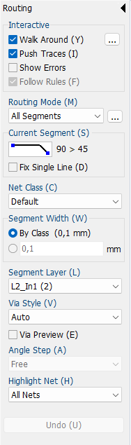
 button on the Route
  button or
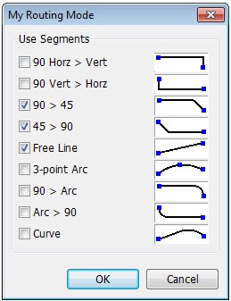
Current Segment. This item serves to change the current trace segment using S hotkey or by selecting the necessary option from the list that appears when left-clicking on the current segment image. The set of available segment types depends on the selected Routing Mode. DipTrace allows drawing orthogonal polylines (90 Horz > Vert, 90 Vert > Horz), polylines with determined vertex angle (90 deg. line > 45 deg. line; 45 deg. line > 90 deg. line) as well as rounded lines (90 deg. line > arc; arc > 90 deg. line) and 3-point arcs. If free line or curve option is selected, the angles of a polyline or the shape of a curve can be defined by the user.
Fix Single Line. This option is applicable to polylines and rounded lines. With this item selected (checkbox on Routing panel or D hotkey), a left click will fix only the first angle-forming segment, placed before the vertex point, leaving the second one in placement mode.
Net Class. Use a drop-down list or C hotkey to choose a net class for a new net created during routing process.
Please note that changing a net class on this panel does not change the class of an existing net. To change the net class of an existing net, open the Net Classes (link to 6.4) dialog-box and change it prior to routing.
Segment Width. The width of the current trace segment is displayed here. Select By class to use the value defined by the Net Class properties or customize this parameter for the current and following segments by typing in the required value. Use W hotkey for a quick access to the list of options for defining the width of the current segment: Net Class, Template, Custom.
Segment Layer. Use the drop-down list on the Routing panel, L hotkey or a layer number from 1 through 9 to change the current routing layer. Additionally, you can use T and B hotkeys to switch to Top and Bottom layer respectively. Trace vias appear automatically.
Via Style. Use a drop-down list or V hotkey to select a via style that will be applied to the vias that appear, if you change the layer when routing a trace. Auto means that DipTrace selects an optimal via style, depending on the situation.
Via preview. Mark the checkbox or use F hotkey to enable/disable this option. When activated, a via that will be placed when changing the trace layer is shown at the tip of the line while routing.
Angle Step. This item is activated when curve or free line is selected as Current Segment. Use drop-down menu or A hotkey to change the angle step to free, 15, 30 or 45 degrees.
Highlight Net. Here you can chose to highlight pads of all nets or only the pads of the current net while drawing a trace. Select the preferred mode or use H hotkey to toggle between the options. Current Net mode is highly recommendable, when Follow rules option is disabled, because it also ensures error-free PCB design by highlighting only those pads and traces that belong to the current net when you hover over them with the mouse pointer in the Manual Routing mode; other traces and pads are basically ignored, making connection to them impossible.
Undo button, same as U or Backspace hotkey, allows undoing the last trace segment.
All the routing parameters are duplicated in and can be adjusted from the right-click submenu when routing a trace.
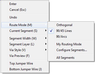
You can use Num Keypad for manual routing of 90/45 segments. First, activate Numpad with NumLock key. Switch on Manual Route mode and left-click in the starting point to begin routing a trace. Use Num keys for routing in the following directions:
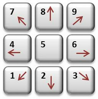
You can finish routing a trace with Numpad by pressing Enter key. It is possible to switch to routing with the mouse and back to Num keys at any moment.
Routing with Numpad is done only with 45/90 segments, irrespective of the current Routing Mode and Segment type.
Routing Setup
Proceed to "Route \ Routing Setup", and select the Settings tab to change more manual routing settings.
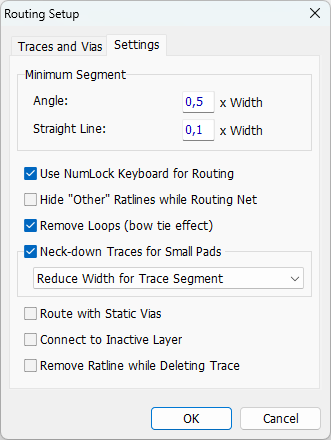
If you want to display all ratlines of the layout while routing the net, uncheck Hide "Other" Ratlines while Routing Net in this dialog box or uncheck "View \ Ratlines \ Routed Net Only" option from the main menu.
Remove Loops – remove bow tie effect when you complete a trace.
Connect to inactive layer – highlight traces in all layers when you hover over them in the Manual Routing mode. This feature is often used with Highlight only current net option because in this case, the software highlights pads and traces of the net being routed regardless of the PCB layer. You do not need to change the layer, via will appear automatically.
Neck-down Traces for Small Pads – when routing the trace which is wider than the pad, DipTrace automatically narrows the trace segment to fit the pad size.
Parameters from the Minimum Segment section are used while editing traces to remove small segments and make straight lines or angles. Default values usually work just fine.
3.5.2.5. Editing traces
Editing traces – moving, adding nodes, changing trace width and layer.
There are two modes of moving traces:
1) Edit existing trace respecting 90- and 45-degree angles. This mode is activated automatically when you try to edit some trace in the Default mode. To enable edit mode manually, go to "Route \ Manual Routing \ Edit Traces" from the main menu or press  button on the Route toolbar. This mode allows the user to move trace segments with 90- and 45-degree angles and to smooth 90-degree "sharp" angles with two angles and a segment, like on the picture below:
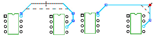
2) Free edit trace. To enable this mode, select "Route \ Manual Routing \ Free Edit Traces" from the main menu or press  button on the Route toolbar. This mode allows for moving trace segments and nodes in any direction anywhere on the design area.
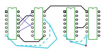
To add a node to a trace segment, hover over it with the mouse, and press N hotkey or right-click, and select Add Node from the submenu. New nodes remain on the trace for several steps until they are automatically removed if unused.
To perform any action with a trace segment, you need to select it first. DipTrace allows the user to select several trace segments at a time with the left mouse clicks (hold Ctrl key and add/remove segments to/from the selection, or use the box selection and Shift key).
All selected segments are displayed by the dotted lines; the Properties tab shows their properties (Ctrl+2 to show/hide the Design Manager).
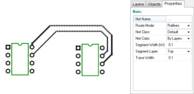
Four segments selected
Press W hotkey or enter a new value into the Segment Width field on the Properties tab. You can also change the trace width. Select the width from the trace templates or set a new value. To change segment layer, select layer from Segment Layer drop-down list on the Properties tab.
Properties tab includes major net properties: change net class, color, route mode, same as in the right-click submenu.
Tab hotkey can be used for smooth trace/ net selection for further editing: select a segment of the trace you want to edit and hit Tab key to toggle between the selection of a segment, trace and net. The function can be applied to various traces/ nets simultaneously.
To delete a segment, right-click it, and select Delete from the submenu.
To unroute segment, trace or net, right-click it, and select Unroute <item> from the submenu.
3.5.2.6. Properties
To open the Net Properties dialog box, right-click on the net trace or pad, and select Properties from the submenu.
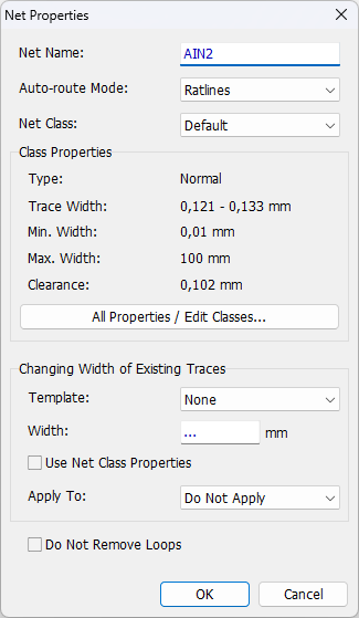
This dialog box allows the designer to change the name, Auto-route mode (see below), and class of the net.
The following Auto-route Modes are available:
Ratlines – existing traces are not changed, and new traces are created, based on a current net structure (this mode is set by default);
Correct Traces – existing traces can be corrected and new ones are placed, based on the net connections;
Full Reroute – unroute all existing traces. New traces are placed, based on the net connections;
Don't Route – do not route this net.
Below the net class selection box, you can preview and edit the net class properties.
Changing Width of Existing Traces section of the Net Properties dialog box allows the user to change the width of selected segments, default segments of the net (if the width is the same as the class properties), selected traces or nets.
Do Not Remove Loops – If the Automatically Remove Loops option is enabled in Routing Setup, it can be overridden for the selected net by enabling this option. This may be useful for power, source, REV, or other nets where loops are intentionally required.
3.5.2.7. Teardrops
Teardrop parameters for trace to pad/via/ trace junctions of the selected objects or all existing junctions of the circuit board are defined in the Add/ Change Teardrops dialog launched by selecting Teardrops item from the Route menu. However, those parameters can be set for individual nets as well.
Right-click on a net and select Teardrops item from the submenu. Check one or several items (Through-Hole Pads and Vias, SMD Pads, T-junctions), for which you want teardrop junctions to be created within the selected net/-s. Define the teardrop parameters as a function of the pad size/ trace width.
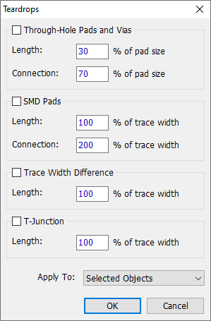
The settings can be applied to the Current Net only or to the Selected Objects.
Note that teardrop settings of individual vias/ pads have priority over those defined for the net.
3.5.2.8. Length matching
DipTrace PCB Layout allows the designer to compare lengths of selected nets automatically and correct the routing using an auto-updated length comparison list. Traces can be compared against each other with a custom tolerance or against a Fixed Length value.
We recommend creating a separate net class and checking the Length Matching by Class box in the Net Classes dialog box if matching tracks of a bus.
Otherwise, you can select "High Speed \ Length Matching" from the main menu or right-click on the track, and select Length Matching, then Open Length Matching from the submenu to set up the constraints, add nets, and create a DRC rule for verification.
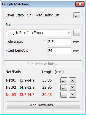
Press Add Net/Pads to select a net and set the starting and ending pads. You can compare lengths of several traces against each other with a Tolerance value (just leave the Fixed Length field empty), or compare them against a target value (enter the Fixed Length parameter). In the latter case, a Tolerance value is automatically divided by two in order to show the ± tolerance above and below the Fixed Length.
Press Create New Rule to save current length-match settings as a DRC rule.Otherwise, the DRC will not verify lengths of the traces.
Notice that you can left-click on several traces with a Ctrl key, and select "Length Matching \ Compare Selected Nets Only" from the submenu to launch the Length Matching tool for selected nets only.
Use the drop-down list in the Rule section to switch between different length-matching rules of the current circuit board. Press the button in the Rule section to rename or delete rules.
Press a corresponding button to replace net or swap its starting and ending pads. Press  to delete net from the list.
DipTrace considers layer stack and pad signal delay when calculating trace lengths. Press the corresponding button at the top of the dialog box to toggle these options.
Meanders
Meander is the most efficient way to make traces longer and length-match them. Press on the High Speed toolbar or select "High Speed \ Add Meander" from the main menu, then left-click on the trace, and drag and drop to create a meander. Meanders are created one at a time. The software helps to create meanders of the same size.
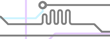
To edit meanders, press button, and drag and drop meander's vertices. To push one or several meanders along the trace, left-click on the trace segment opposite the preferred direction, and drag and drop several meanders.
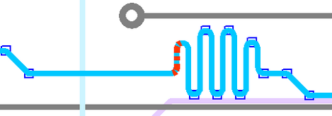
Notice that you can also use the Add Meander mode ( button) to edit meanders.
By default, the gap between the meanders is defined by the net class clearance. To set custom meander gap, right-click on the trace, and select Meander Gap from the submenu. In the pop-up dialog box, check Value box, enter new gap, and press OK.
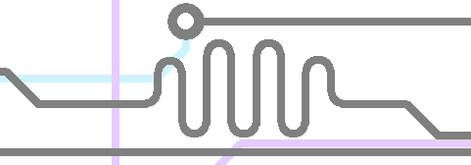
3.5.2.9. Signal delay
Bond wires are the wires inside electronic component's package, which connect pads to the die. These wires introduce a signal delay, which should be accounted for in high-speed designs. Manufacturers report this in-device pad signal delay in the datasheets in picosecond time or as a length.
Pad signal delay value is considered for phase tuning and length matching, it is added to the total length of tracks. We recommend setting up signal delays for a component in the DipTrace Component Editor, but you can also set it in the Schematic and directly in the PCB Layout (delay value is valid only for this schematic and PCB, it does not affect the component in the library).
To set a pad signal delay in the PCB Layout, right-click on the component and select Pad Signal Delay from the submenu or right-click on the pad, and select Signal Delay.
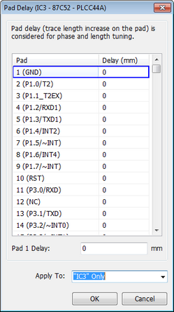
Select pad from the list (if not selected already), and enter a signal delay right below. Select if you want to apply this parameter only to the selected component or to all components with the same name on the circuit board. Press OK to apply changes.
Use Shift + U hotkeys to change the measurement units on the go.
You can also assign pad signal delays in DipTrace Schematic and Component Editor (recommended).
3.5.2.10. Trace vias
DipTrace has two logical types of vias: Trace Via and Static Via. Trace via is part of a trace, while a static via has more parameters and behaves like a pad.
Regular or Trace Via automatically appears between two trace segments located on different layers. Vias (regardless of their logic type) always belong to a via style, which determines its physical type (through-hole or blind/buried), dimensions and layers (for blind/buried vias).
To change trace via, right-click it, and select Via Properties from the submenu.
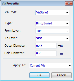
In the pop-up dialog box change the via style, type, dimensions and layer pair for blind/buried vias, then select the way to apply these changes: current via, selected segments, selected traces or nets.
Notice that DipTrace can offer you to create a new via style if there is no via style with such parameters.
Trace vias can be easily converted to static vias: right-click on the via, and select Convert Via to Static from the submenu.
3.5.3. Via
3.5.3.1. Review
DipTrace has two logical types of vias: Trace Vias and Static Vias.
Trace Vias are technically parts of traces. They automatically appear and disappear when you move trace segment between the PCB layers. When you move traces, trace vias also move.
Static Vias are very similar to pads. You can place static vias without creating traces to connect SMD pads to plane layers or connect two copper polygons on different layers.
All vias in DipTrace, regardless of their logic type, belong to certain via styles. Via style determines via type, dimensions, and layers (for Blind/Buried).
3.5.3.2. Via styles
The layout may have several via styles with different properties. All vias regardless of their logic type (trace via or static via) belong to particular via style (Default). Via style determines the following properties: via type (through-hole or blind/buried), layers (for blind/buried vias), outer diameter (copper ring) and hole diameter. To create/edit a via style, select "Route\ Via Styles" from the main menu. The following dialog box will pop up:
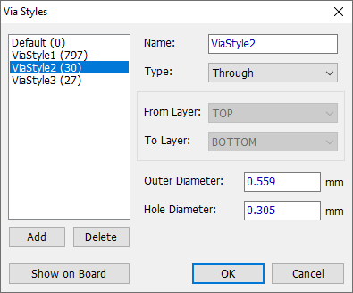
Here you can add/delete via styles and edit their properties. If you try to delete a via style, choose a new one for the vias that belong to it in the pop-up dialog box.
The first via style is always Default and through-hole, you can not remove it or change its type, but you can change via diameters. Notice that you can also edit Default via style in the Routing Setup dialog box.
Press Show on Board button and DipTrace will display Show Vias by Style dialog, where you can select a via style and localize its vias on the board.
3.5.3.3. Placing vias
Trace via automatically appears when you move trace segment between the circuit board layers.
To place a static via, go to "Objects \ Place Static Via" from the main menu or press  button on the Elements toolbar. You can change default static via properties on the Design Manager panel when Place Static Via tool is active.
In manual routing mode DipTrace allows previewing vias selected for the trace being routed before placing them. To enable this option, use F hotkey or check Via Preview box on the Routing panel. A via contour with defined parameters will appear at the tip of the placed segment.
3.5.3.4. Properties
Via style defines all physical via properties: type, layers, and dimensions. To change via style for existing via or edit settings separately, right-click on the via, and select Via Properties from the submenu.
In this dialog box you can change via style and dimensions, then select where to apply changes (Apply To drop-down list). If no similar via style exists, DipTrace suggests to create a new via style.
3.5.3.5. Convert trace via to static
To convert trace via to static, right-click it, and select Convert Via to Static from the submenu. Apply it to current via, selected segments, selected traces or all vias.
To convert a static via to trace via, right-click it, and select Convert to Trace Via. Apply to current via, selected vias or all vias. Unconnected vias or vias with one trace can not be converted. If all connected traces are on the same layer, the vias automatically disappear.
3.5.3.6. Thermal settings
Static vias can have custom thermal settings (different from the copper pour properties). Right-click on the static via, and select Thermal Settings from the submenu.
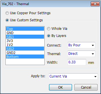
In the pop-up dialog box, the Use Copper Pour Settings box is checked by default. This means that common copper pour settings apply to this static via.
Check Use Custom Settings, and define custom thermal settings for the Whole Via or By Layers.
Other fields:
Connect means that you can remove or add a thermal connection for the via regardless of the net in the copper pour settings.
Thermal is a thermal connection type applied.
Width is a spoke width used for non-direct connection types.
Apply settings current via only, to all vias of the same style, or to selected vias.
3.5.3.7. Via Shielding
A via shield is created by placing one or more rows of vias along a trace and is used to isolate areas of the board that operate at different frequencies. To apply via shielding, right-click on a trace and select Via Shielding from the submenu or go to Objects/ Via Tools/ Net Via Shielding.
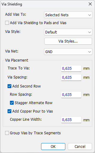
In the pop-up dialog you can choose to Add Vias to Selected Segments, Traces or Nets.
Mark Add Via Shielding to Pads and Vias to include shielding for pads and vias.
Select Via Style from the drop-down or click the Via Style button to view, modify, or create new via styles.
In the Via Net drop-down select the net to which the shield vias will be connected.
Define Trace to Via and via to Via Spacing.
Mark Add Second Row to create a two-row shield. Set the Row Spacing. Enable Stagger Alternate Row to to arrange the vias in a staggered pattern.
Mark Add Copper Pour to Vias to shield a trace with copper pour line in addition to vias. Set the Copper Line Width as needed.
Group Vias by Trace Segments option groups vias that shield different trace segments for better organization.
Once your settings are configured, click OK to apply the via shielding or Cancel to discard the changes.
To remove Via Shielding go to Objects/ Via Tools/ Remove Via Shielding and select whether to remove it from Selected Traces, Nets, or Segments.
3.5.3.8. Via Stitching
Via Stitching is used to connect copper areas on different layers to ensure short return paths for signals or to help maintain a constant ground. Via stitching is conducted after the primary layout and routing of the board are completed. Overlapping copper regions connected to the same net can be filled with stitching vias.
DipTrace allows for stitching copper pours on a defined area or the entire board.
To define the area to be stitched with vias go to Objects/ Via Tools/ Area Via Stitching and outline the area, right-click in the final point and select Enter.
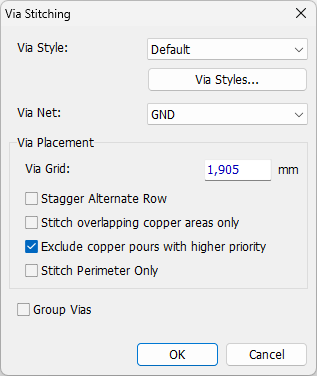
In the pop-up dialog select Via Style from the drop-down or press Via Style button to check the parameters of the existing via styles or create a new one.
In the Via Net drop-down select the net the stitching vias will be connected to.
Specify the Via Grid and mark other Via Placement options, where necessary:
Stagger Alternative Row to shift the vias in alternative rows;
Stitch overlapping copper areas across layers;
Exclude copper pours with higher priority;
Stitch Perimeter Only.
Mark Group Vias to group all stitching vias.
3.5.3.9. Teardrops
Teardrop parameters for trace to pad/via/ trace junctions of the selected objects or all existing junctions of the circuit board are defined in the Add/ Change Teardrops dialog launched by selecting Teardrops item from the Route menu. However, those parameters can be set for individual vias as well.
Right-click on a via and select Teardrops item from the submenu. Tick Through-Hole Pads and Vias checkbox and define the teardrop Length and width in the Connection area as a percentage of the pad size.
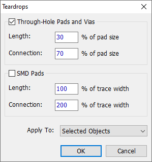
The settings can be applied to the Current Via only or to the Selected Objects.
Note that teardrop settings of individual vias have priority over those defined for the net.
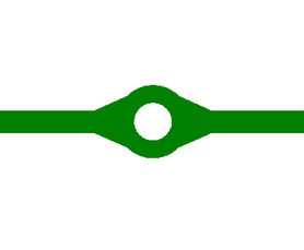
3.5.3.10. Mask and paste settings
Default solder mask and paste settings for all pads and vias on the circuit board are defined in the Gerber export dialog box. However, static vias (like pads) can have custom properties in the solder mask and paste layers. Right-click on the static via, and select Mask / Paste Settings to change custom solder mask/paste properties.
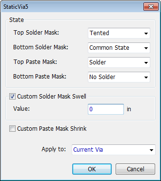
Select the state of the top/bottom solder mask/paste of the via, using respective drop-down lists in the State section of the dialog box.
Common state – apply default solder mask and solder paste parameters to the via;
Open – via not covered with solder mask regardless of the default parameters;
Tented – via covered with solder mask regardless of the default parameters;
By Paste Mask – solder mask will match Paste Mask;
Solder – apply solder paste to the via regardless of the default parameters;
No Solder – do not apply solder paste to the via regardless of the default parameters;
Segments – allows splitting paste into segments. With this option selected you can define fill percent, min. segment side, min.segment gap and nominal edge gap for the paste mask segments.
If you need custom solder mask swell and paste mask shrink settings for the via/s, check the respective check boxes, and enter custom values (negative numbers are supported).
Changes can be applied to the current via, to all vias of the same style, or to the selected vias.
3.5.4. Differential pair
3.5.4.1. Review
DipTrace provides tools to create and edit differential pairs on the schematic and directly in the PCB Layout module. Assign differential pair declaration to any nets that exist on the design area.
Net classes manage all differential pair properties and routing constraints. Create a special net class of Differential Pair type before defining a differential pair. Differential pairs are not allowed to have parameters outside differential pair net classes. Differential pair parameters are verified as DRC constraints.
Routing differential pair is fairly simple (simultaneous two-track mode or single-track routing mode).
External autorouting via DSN/SES interface.
3.5.4.2. Create differential pair
To create a differential pair, proceed to the Net Classes dialog box ("Route \ Net Classes" from the main menu), and create a new net class.
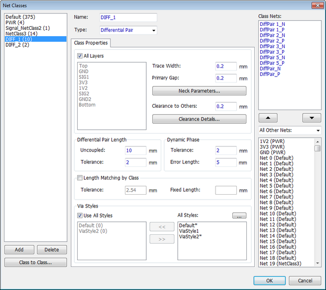
Press Add button, and select Differential Pair Type. Class properties allow the user to change trace width, primary gap between the traces, clearances to other objects, differential pair length, and dynamic phase settings.
Necking parameters allow the user to route a differential pair in narrow places. Press Neck Parameters to define neck track width, gap, and maximum length of the neck-down segment. DRC takes Net Class parameters (including Neck Settings) as design constraints.
Press OK to close the Net Classes dialog box.
Now go to "High Speed \ Define Differential Pair" from the main menu.
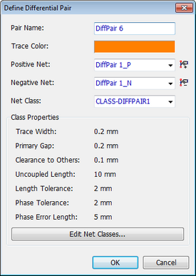
In the pop-up dialog box, change pair name, color, and define positive and negative nets of the pair with the corresponding drop-downs or by pinpointing nets directly on the design area with  or
or  buttons.
Notice that a previous net name is disregarded for a new one, typically it consists of a diff pair name + positive or negative net identifiers.
Press Edit Net Classes button to open the Net Classes dialog box.
Differential pair pads are marked with special symbol directly on the design area. Custom differential pair color also applies to pads of the pair.
3.5.4.3. Route differential pair
DipTrace allows the user to route two tracks simultaneously or one by one.
Double-track routing
Routing a differential pair is very similar to routing regular nets. Press button on the Route toolbar, or use Tilde sign (~) hotkey, then left-click on any of the differential pair pads, and start drawing the traces. Two tracks of the pair with specified gap appear on the design area simultaneously.
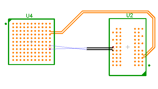
Left-click on the key point of the track to create a node, use Routing panel on the left for any on-the-go customizations. Please refer to Routing Traces topic for manual routing basics, which are also applicable to differential pairs.
Single-track routing
Sometimes you need to separately route each track of the pair in order to succeed. When in the differential pair manual routing mode, right-click, and select Route Single Trace from the submenu, then continue drawing a track to its pad.
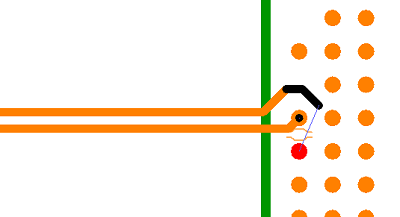
In order to change the track being routed, select Change Control Trace from the right-click submenu.
If you want to return to pair routing, select Route Pair from the right-click submenu. When one of the pair tracks is routed, DipTrace automatically switches to the unrouted net.
3.5.4.4. Neck differential pair
Go to Net Classes dialog box ("Route \ Net Classes" from the main menu), select the differential pair net class, and press Neck Parameters button.
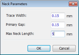
Enter the trace width and gap between the traces. Max Neck Length parameter allows the user to define the maximum length of a necked trace segment. If a necked segment is longer than this value, the DRC drops an error.
When routing differential pair on the design area, right-click, and select Neck-down Segment from the submenu, or use W hotkey.
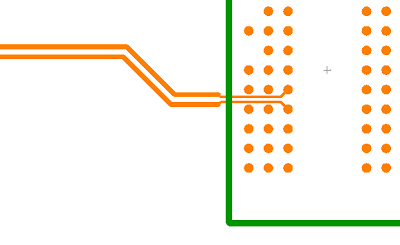
To return to normal width, select Return to Regular Width from the right-click submenu.
3.5.4.5. Edit differential pair
Editing differential pair traces – moving tracks, adding nodes, changing the width and layer of the tracks.
Editing of routed differential pairs is quite similar to editing single tracks (if you are new to the software, read that topic first), the only difference is that with differential pairs you can edit two tracks simultaneously or each track separately from the other.
Editing as a pair
Go to "Route \ Manual Routing \ Edit Traces" from the main menu or press button on the Route toolbar. This is a regular track edit mode that allows the user to move two tracks of a differential pair simultaneously with respect to 90- and 45-degree angles. The differential pair, in this case, behaves just like a single trace. Select tool to simultaneously edit two tracks of the pair without any constraints.
To add a node to the traces, move the mouse pointer over the trace segment, and press N hotkey or right-click, and select Add Node from the submenu. New nodes remain on the traces for several steps until they will be automatically removed if unused.
In order to change the differential pair name, color, unroute any part of the pair, change layer of the segment, trace, or entire differential pair, just right-click on the trace, and select the corresponding item from the drop-down list.
Basic differential pair properties are available on the Properties tab of the Design Manager when a differential pair is selected.
Single-trace editing mode
For single track editing, go to "High Speed \ Differential Pair Tools", then select Edit Single Trace for editing a single trace with respect to 90- and 45-degree angles, or select Free editing of Single Trace.
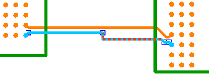
You can also use the and buttons to launch the respective single-trace editing modes.
3.5.4.6. Phase tuning
Net Class settings control a maximum uncoupled length of a differential pair, length tolerance for the two tracks of a pair, dynamic phase tolerance and the maximum length of a segment with dynamic phase tolerance violation. DRC verifies the circuit board according to these parameters. If the DRC reports a phase shift (dynamic phase tolerance violation), select the Phase Tune tool to find the problem and ensure that the timing of the differential pair signals is correct.
The height of vias (derived from the Layer stack) and pad signal delay (the length of inner-component bonding wires) are considered by the Phase Tuning tool.
Press  button on the High Speed toolbar, or select "High Speed \ Differential Pair Tools \ Phase Tune" from the main menu. The following dialog box pops up:
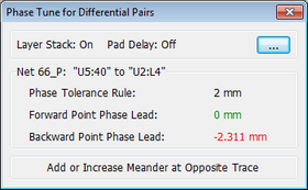
With Phase Tune tool active you can hover over the differential pair trace and check if there is a phase delay or hurry on a particular trace segment counting from both ends of the trace in forward and backward directions. The software also points you to the segment where meanders needed in order to fix a phase shift.
DipTrace considers a signal delay on the pads and via height determined by the layer stack when calculating trace length and signal phase.
Left-click on the segment, and drag and drop to create a meander. Meanders are created one at a time. The software helps to create meanders of the same size. Meanders reduce the phase timing difference between the two tracks of a differential pair. You can control a current phase shift value in the Phase Tune for Differential Pairs dialog box.
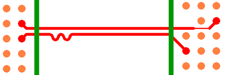
Find out more about adding and editing meanders in the Length Matching topic.
3.5.4.7. Signal delay
Bond wires are the wires inside electronic component's package, which connect pads to the die. These wires introduce a signal delay, which should be accounted for in high-speed designs. Manufacturers report this in-device pad signal delay in the datasheets in picosecond time or as a length.
Pad signal delay value is considered for phase tuning and length matching, it is added to the total length of tracks. We recommend setting up signal delays for a component in the DipTrace Component Editor, but you can also set it in the Schematic and directly in the PCB Layout (delay value is valid only for this schematic and PCB, it does not affect the component in the library).
To set a pad signal delay in the PCB Layout, right-click on the component and select Pad Signal Delay from the submenu or right-click on the pad, and select Signal Delay.
Select pad from the list (if not selected already), and enter a signal delay right below. Select if you want to apply this parameter only to the selected component or to all components with the same name on the circuit board. Press OK to apply changes.
Use Shift + U hotkeys to change the measurement units on the go.
You can also assign pad signal delays in DipTrace Schematic and Component Editor (recommended).
3.5.4.8. Remove differential pair
To remove a differential pair declaration from the nets:
1. Use the Differential Pair Manager ("High Speed \ Differential Pair Manager" from the main menu). In the pop-up dialog box select a differential pair, and press Delete button.
2. Right-click on the track or any pad of the differential pair, and select Remove Diff Pair from the submenu.
Removing the differential pair declaration does not remove the nets or unroute tracks. DipTrace will return original net names.
Notice that if you select a differential pair trace, and press the Del hotkey, or right-click, and select Delete from the submenu, you completely delete a differential pair nets from the design.
3.5.4.9. Define paired pads
On rare occasions, DipTrace might not be able to finish routing the differential pair. The software displays the warning message that offers to use Define Paired Pads feature. The most typical error-prone situation is when each net of the differential pair terminates on two closely-located pads.
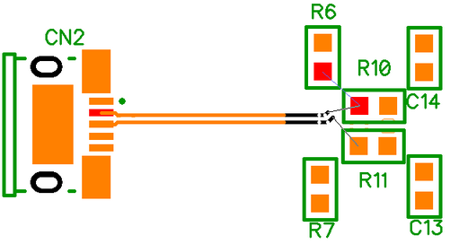
In the situation on the picture above, DipTrace offers to terminate traces on the wrong pads. To fix the issue, you need to let the software know the correct pair of terminal pads. Go to "High Speed \ Define Paired Pads" from the main menu.
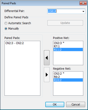
Using the Differential Pair drop-down list, select the differential pair that you have problems with. If Automatic Search is checked, press Update and new pad pairs should appear in the Paired Pads list right below.
If no success with Automatic Search, then check Manually item, and select the pair of the pads from the lists showing the unpaired pads (Positive Net and Negative Net). Then press the left arrow button to pair the pads.
3.5.4.10. Diff pair properties
Right-click on a differential pair or pads that belong to a differential pair net, and select Diff Pair Properties from the submenu.
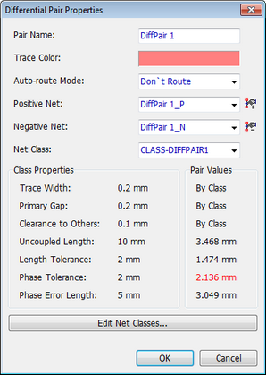
In the pop-up dialog box, you can change the differential pair name, the color of the traces, put the differential pair declaration on other nets or assign a new net class. Required parameters of the net class and current parameters of the routed differential pair are right below. Violations are highlighted in red.
Press Edit Net Classes to open the standard Net Classes dialog box for adding/deleting/editing net classes.
There are several ways to edit differential pair properties:
1. Go to "Route \ Net Classes" from the main menu, and select respective differential pair net class to edit its parameters;
2. Right-click on any differential pair on the design area, and select Differential Pair Properties from the submenu.
3. Use the Differential Pair Manager ("High Speed \ Differential Pair Manager" from the main menu).
3.5.4.11. Differential Pair Manager
Differential Pair Manager is the most convenient way to create/edit/delete differential pairs. Go to "High Speed \ Differential Pair Manager" from the main menu. The following dialog box pops up:
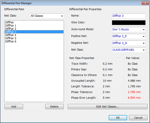
Sort differential pairs by net classes, then select a differential pair from the list to review and change all parameters. Press Edit Net Classes to open the standard Net Classes dialog box for adding/deleting/editing net classes. In order to add or delete a differential pair, use Add or Delete buttons. Press OK to apply changes.
3.5.5. Shape
3.5.5.1. Review
Shapes allow the designer to create any custom drawing on different circuit board layers, use one or several shapes to define a board outline, cut custom holes in the board (board cutouts) and limit routing/placement in some areas (Route Keepout and Place Keepout).
The following shape types are available: Line, Arc, Rectangle, Filled Rectangle, Obround, Filled Obround, Polyline and Polygon.
Place shapes on silk, assembly, component outline, courtyard, mask, paste, board outline, copper (Signal and Plane), Route Keepout, Placement Keepout layers.
3.5.5.2. Create
To create a shape, press  on the Drawing toolbar, select a corresponding shape object, and draw it on the design area.
To place a Line, press button on the Drawing Toolbar and select  . Left-click to anchor the starting point and the end point. When drawing the line, it’s dimensions will be displayed by DipTrace.
To place an Arc, press button on the Drawing Toolbar and select  . There are three modes for Arc placement in DipTrace. Left-click to anchor the starting point, then right-click to select the mode:
Start - Center - Angle - with this mode selected an arc with a certain angle is built based on a circle with defined radius. Anchor the starting point, the center point of a circle will appear; the radius of the circle is equal to the distance between the starting point and the center point. Move the center point away from the starting point to get a circle with desired parameters. Next left-click and adjust the angle of the arc. Left-click to anchor the end point of the arc.
Start - End - Radius - in this mode an arc of desired radius is built between the Start and End points. Place the Start and End Points and move the mouse pointer to adjust the radius of the arc. Left-click when done.
Start - End - Middle Point - in this mode an arc is built based on three points. Place Start and End point, the third point will appear on the line between them. Move the point to get an arc with desired parameters.
Choose Clockwise or Counter-Clockwise from the right-click submenu to set the concavity direction of the curve.
Select Cancel from the right-click submenu to cancel the arc placement.
When drawing an arc, it’s key parameters (radius, deg.) will be displayed by DipTrace.
To place a Rectangle/ Filled Rectangle, press and select  or
or  respectively on the Drawing Toolbar. Left-click to anchor the starting point, draw the shape and left-click in the end point. When drawing the shape, it’s dimensions will be displayed by DipTrace.
To place a Obround/ Filled Obround shape, press and select  or
or  button respectively on the Drawing Toolbar. Left-click to anchor the starting point, draw the shape and left-click in the end point. When drawing the shape, it’s dimensions will be displayed by DipTrace.
To place a Polyline/ Polygon, press and select  or
or  button respectively on the Drawing Toolbar. Left-click to anchor the starting point, draw the shape, left-click to anchor points, right-click in the end point and select Enter form the submenu. When drawing the shape, it’s dimensions will be displayed by DipTrace.
To change default line width and font for newly placed shape objects, select Objects/ Drawing Properties/ Line Width from the main menu. To set default line width by layers, go to View/ Line Width.
When you create a shape on the design area, it appears in the corresponding layer, selected from the drop-down list on the Drawing toolbar. However, you can change a layer once a shape is on the design area (in the Shape Properties dialog box).
3.5.5.3. Edit
To change shape size, select a shape, and move its key points with the left mouse button. When editing a shape, it’s dimensions will be displayed by DipTrace in real time.
For precise editing of the shape, use the Shape Properties dialog box.
3.5.5.4. Properties
3.5.5.4.1. Line
Right-click on a line, and select Properties from the submenu to open Shape Properties dialog box:
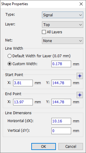
Here you can change the shape Type. If Signal or Route Keepout type is selected from the list, a Layer drop-down appears to specify the layer as well as All Signal Layers checkbox – tick it, if you want the shape to be placed on all signal layers. Use Net drop-down to connect shape to a certain net (assigning shape to net allows for avoiding the DRC errors).
You can choose to use default line width for the selected Layer; or customize it for the given shape.
Start and End Points can be adjusted by changing X and Y coordinates or by using  button to set them by Mouse Pointer.
Finally, you can edit Line Dimensions, just type-in new values for Horizontal (dX) and Vertical (dY) tangent.
3.5.5.4.2. Arc
Right-click on an Arc, and select Properties from the submenu to open Shape Properties dialog box:
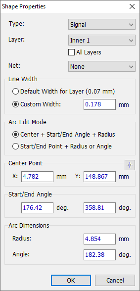
Here you can change the shape Type. If Signal or Route Keepout type is selected from the list, a Layer drop-down appears to specify the layer as well as All Signal Layers checkbox – tick it, if you want the shape to be placed on all signal layers. Use Net drop-down to connect shape to a certain net (assigning shape to net allows for avoiding the DRC errors).
You can choose to use default line width for the selected Layer; or customize it for the given shape.
Select an Arc Edit mode: Center+Start/End Angle+Radius or Start/ End Point+Radius or angle. Type-in all the required values. Note that points can be defined by X and Y coordinates or set by Mouse Pointer upon pressing .
Finally, you can change arc Radius and Angle.
3.5.5.4.3. Rectangle/ Filled Rectangle
Right-click on a Rectangle/ Filled Rectangle, and select Properties from the submenu to open Shape Properties dialog box:
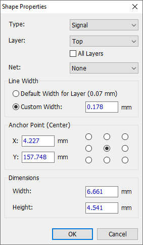
Here you can change the shape Type. If Signal or Route Keepout type is selected from the list, a Layer drop-down appears to specify the layer as well as All Signal Layers checkbox – tick it, if you want the shape to be placed on all signal layers. Use Net drop-down to connect shape to a certain net (assigning shape to net allows for avoiding the DRC errors).
You can choose to use default line width for the selected Layer; or customize it for the given shape.
Next, you can change the position of an anchor point and type-in its coordinates.
Finally, you can edit shape dimensions.
3.5.5.4.4. Obround/ Filled Obround
Right-click on an Obround/ Filled Obround shape, and select Properties from the submenu to open Shape Properties dialog box:
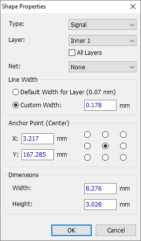
Here you can change the shape Type. If Signal or Route Keepout type is selected from the list, a Layer drop-down appears to specify the layer as well as All Signal Layers checkbox – tick it, if you want the shape to be placed on all signal layers. Use Net drop-down to connect shape to a certain net (assigning shape to net allows for avoiding the DRC errors).
You can choose to use default line width for the selected Layer; or customize it for the given shape.
Next, you can change the position of an anchor point and type-in its coordinates.
Finally, you can edit shape dimensions.
3.5.5.4.5. Polyline/ Polygon
Right-click on a Polyline/ Polygon shape, and select Properties from the submenu to open Shape Properties dialog box:
|
|
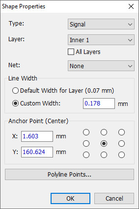
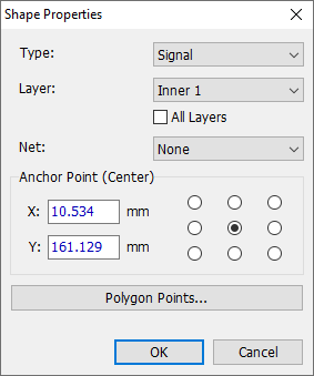
Here you can change the shape Type. If Signal or Route Keepout type is selected from the list, a Layer drop-down appears to specify the layer as well as All Signal Layers checkbox – tick it, if you want the shape to be placed on all signal layers. Use Net drop-down to connect shape to a certain net (assigning shape to net allows for avoiding the DRC errors).
You can choose to use default line width for the selected Layer; or customize it for the given shape.
Next, you can change the position of an anchor point and type-in its coordinates.
Finally, you can edit shape dimensions by clicking on Polyline Points/ Polygon Points button.
3.5.6. Text
Enter topic text here.
3.5.6.1. Review
DipTrace supports placing a multi line text.
Text object can be placed on assembly, silk, outline, courtyard, mask, paste, board outline, copper (Signal and Plane), Route Keepout, Placement Keepout layers. It can be connected to a net, if placed on a sygnal/ plane layer.
3.5.6.2. Create
To create a text go to Objects/ Place Text or press  button on the Drawing toolbar.
Left-click on the design area and type the text.
Use Enter key to move to the next line.
Right-click on a free spot of the design area to return to default mode. You can drag and drop the text to change its location; guidelines will appear while moving the text to help you align it with other text objects.
To define text font type, size and other parameters before placement, select Objects/ Drawing Properties from the main menu. However, it is possible to change these properties for objects already placed on the design area.
Note that tilde (~) before and after text is reserved by the software for placing a line over the pin name, which implies inversion; if you want a tilde symbol to appear as it is, you should place it twice:
~text~/~~text

3.5.6.3. Edit
To edit, double click on the text object or right-click on it and select Edit Text. The following dialog will appear:
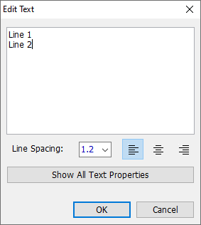
Here you can change the text, line spacing and alignment. Press Show All Text Properties button to access Text Properties dialog that allows for adjusting more text object parameters.
Text Rotation
Several Text rotation options are available, they can be accessed from the text right-click submenu:
Rotate – rotation at 90-degree step counter-clockwise. You can use R or Space hotkeys for the same purpose.
Rotate by Angle – select a preset angle of rotation or customize it.
Free Rotate – this option allows rotating text by any angle in real time.
You can also set text rotation angle in Text Properties dialogue.
Hover over the test object and drag it to another location.
To delete a text, right-click it, and select Delete from the submenu.
Text parameters can be changed in the Picture Properties dialogue.
3.5.6.4. Properties
To open Text Properties dialog, right-click on the text object and select Properties from the submenu.
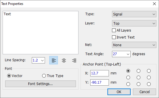
In the pop-up dialogue you can set line spacing, text alignment and font, define its type and the layer it belongs to. If Signal or Route Keepout type is selected from the list, a Layer drop-down becomes active, where you can specify the signal/plane layer, as well as All Signal Layers checkbox – tick it if you want the text to be placed on all signal layers. You can use invert text option to etch text in copper pour, or make it as void in silk screen. Use Net drop-down to connect text to a certain net (this option is available only if Signal Type has been selected). Choose an angle from the Text Angle drop-down or just type-in the required value to rotate the text.
The location of the Anchor Point of the text box is set by ticking the respective circle. Anchor Point is displayed as a cross. You can also set the coordinates of the Anchor point.
Press Font Settings button to open Font dialog (it can also be accessed by selecting Font in the text right-click submenu):
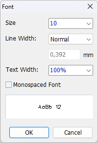
Here you can set the font size, select the Line Width from Thin, Normal, Bold or Customize it, and also define the Text Width.
Mark Monospaced Font to distribute character spacing evenly across the text. Applicable to vector fonts only.
3.5.7. Picture
3.5.7.1. Review
In DipTrace images can be placed on any layer, available for shape placement.
A vectorized picture can be connected to a net, if placed on a sygnal/ plane layer, and merged with copper pour.
Raster image can be placed only as a reference template associated with Assembly layer; it is not included into manufacturing documentation.
3.5.7.2. Create
To place a picture go to Objects/ Place Picture or press  button on Drawing toolbar.
Define the border box for the image on the design area – a file selection dialog box pops up automatically. Select the required image file and click Open.
In the pop-up Picture Vectorizing window you can choose Background Color (select white to have the image shown on your layout or black, if you want to invert it and make it as void in silk screen or copper pour) and adjust the Tolerance. Click OK.
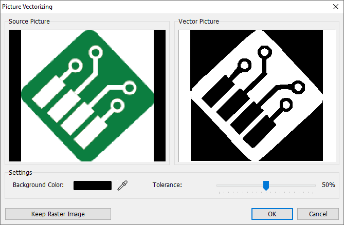
If you are opening a raster image and do not want to vectorize it, press Keep Raster Image button. Note that raster images will be placed as a template that will not be included into manufacturing documentation.
The program supports BMP and JPEG formats of raster images.
The image is placed in the layer selected from the drop-down on the Drawing panel.
Right-click in the on a free spot of the design area to return to default mode.
3.5.7.3. Edit
To change the image size, left-click on one of its key points and drag, length and width will change proportionally.
Several Picture rotation options are available, they can be accessed from the picture right-click submenu:
Rotate – rotation at 90-degree step counter-clockwise. You can use R or Space hotkeys for the same purpose.
Rotate by Angle – select a preset angle of rotation or customize it.
Free Rotate – this option allows rotating image by any angle in real time.
You can also set picture rotation angle in Picture Properties dialogue.
Hover over the picture object and drag it to another location.
To delete a picture, right-click it, and select Delete from the submenu.
Image parameters can be changed in the Picture Properties dialogue.
3.5.7.4. Properties
To open Picture Properties dialog, right-click on the picture and select Properties from the submenu.
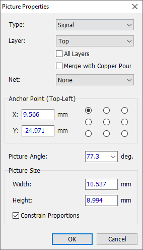
In the pop-up dialogue you can define its type and the layer it belongs to. If Signal or Route Keepout type is selected from the list, a Layer drop-down becomes active, where you can specify the signal/plane layer, as well as All Signal Layers checkbox – tick it if you want the picture to be placed on all signal layers. Check Merge with Copper Pour option to etch the image in the copper pour. Use Net drop-down to connect picture object to a certain net (this option is available only if Signal Type has been selected).
You can also select an Anchor Point location and set the angle of rotation from the drop-down or type-in a custom value.
Define the Width and Height of the picture. Use Constrain Proportion checkbox to enable/ disable maintaining the image proportions. With Constrain Proportion option disabled the image key points on the right allow changing the width and the bottom-left point - adjust the height of the picture.
DipTrace supports BMP and JPEG formats of vector images.
All pictures are saved as vector images in the PCB project file.
3.5.8. Table
3.5.8.1. Review
A table has a certain number of columns and rows. Table field can contain any text aligned to the left, center or right side of the field.
To change the column width or row height, use the Table Properties dialog box or select the corresponding item from the table right-click submenu.
To change text and alignment, click on the corresponding table cell, then type in the text and change alignment in the pop-up dialog box.
Place tables in assembly or silk layers. Table layer is defined when the table is placed. To change layer of an existing table, right-click on the table, select Properties, and select new layer in the Table Properties dialog box.
3.5.8.2. Create
Select "Objects \ Place Table" from the main menu or press button on the Elements toolbar, then left-click on the design area to place a table.
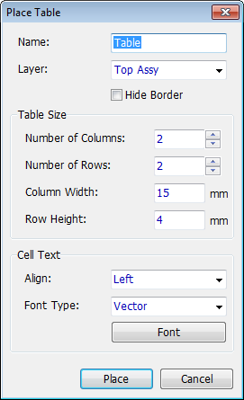
In the pop-up dialog box, specify the table name, layer (Top Assembly, Top Silk, Bottom Silk, or Bottom Assembly, etc.), set the number of columns and rows, column width and row height, alignment, font, and press the Place button.
To define the text inside the table cell, left-click on the corresponding table cell, and enter the text, change the font and alignment for the cell in the pop-up dialog box.
Change general table properties in the Table Properties dialog box.
3.5.8.3. Edit
To define text, font, and alignment of the table cell, as well as column width and row height, click on the table cell, and change properties in the pop-up dialog box.
You can also change the column width and row height if you right-click on the corresponding table cell, and select Column Width or Row Height, and enter new values in the pop-up dialog boxes. To change the size of all columns and rows of the table, use the Table Properties dialog box.
To add columns and rows to the table hover over the table border, right-click it, and select the corresponding items from the submenu.
To insert columns or rows to the table hover over the table field, right-click it, and select the relevant item from the submenu. Empty columns or rows appear before the current cell.
To delete columns or rows from the table, right-click on the corresponding cell, and select Delete Column or Delete Row from the submenu.
3.5.8.4. Properties
To change table properties, right-click it, and select Properties. The following dialog box pops up:
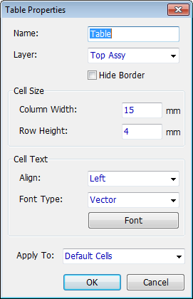
Here you can change table name, layer (Top Assembly, Top Silk, Bottom Silk or Bottom Assembly, etc.), column width, row height, alignment and font by default.
Apply changes to:
– all table cells;
– cells with default settings;
– new cells only (not applied to existing cells).
3.5.8.5. Saving to the file
A table can be saved to Excel CSV file or into the formatted text file.
To save the table into the file, right-click it, and select Save to File from the submenu.
Open the CSV files in any spreadsheet editors like MS Excel or OpenOffice, etc.
3.5.9. Copper pour
To place a copper pour, select "Objects \ Place Copper Pour" from the main menu or press  on the Elements toolbar, then click on the design area to define the key points of the copper pour polygon, and right-click, and select Enter from the submenu, or press Enter hotkey.
In the pop-up dialog box, you can specify the following parameters:
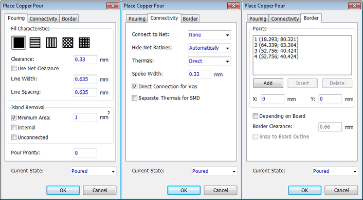
Tabs:
Pouring
Fill Type – type of the copper pour fill (Solid, Horizontal Lines, Vertical Lines, Cross 45, or Cross 90)
Clearance – minimum gap between signal/plane layer objects and the copper pour.
Use Net Clearance – if checked, the software takes the clearance value from the Net Class parameters of the current net.
Notice that this option does not affect the clearances of neighboring objects (other traces and copper pours).
Line Width – size of the lines forming the copper pour. It is one of the basic copper pour parameters.
Line Spacing – line-to-line spacing in the copper fill (for non-solid fill types).
Island Removal – define the minimum area of the copper pour island (the software will remove all smaller islands), remove all internal islands, remove all unconnected islands.
Pour Priority – this option helps to organize several copper pours on a PCB layer. Lower value in the field means higher priority level.
For example, "Pour Priority: 0" defines the most important polygon, copper pours with "Pour Priority: 1" change depending on the borders of the polygon with higher priority, and so on.
Current State – current state of the copper pour. There are two states: poured and unpoured, select poured state or update unpoured copper pours before printing or ordering the circuit board because unpoured copper polygons are not considered as copper areas.
Connectivity
Connect to Net – connect selected net to the copper pour.
Hide Net Ratlines – different options for displaying the ratlines of the copper pour net:
Automatic – the software hides the ratlines for connected segments and displays the ratlines for unconnected segments;
Do not Hide – ratlines are always visible;
All Ratlines – all ratlines are always invisible, regardless of their status (connected or not).
Thermals – select a thermal connection between the pads and the poured area.
Notice that pads and vias can have custom thermal settings.
Spoke Width – width of connection lines for non-direct thermals.
Direct Connection for Vias – directly connect all vias to the copper pour (without thermals).
Notice that this option does not override custom thermal settings of the vias.
Separate Thermals for SMD – separate thermal settings for SMD pads.
Border
Points – define copper pour polygon points by specifying their coordinates.
Depending on Board – if checked, the copper pour polygon covers an entire board. In this case clearance to the board outline can be specified right below.
Snap to Board Outline – if checked, the copper pour changes in real-time when you edit the board outline.
To change parameters of the copper pour, right-click on the copper pour border, and select Properties from the submenu. To set the Poured state, right-click on the copper pour border, and select Update or "State \ Poured" from the submenu.
Go to Objects menu and select Update All Copper Pours to update all copper pours of the board in one click, select Clear All Copper Pours to unpour all copper pours on all layers.
To define separate thermal settings for the pad/static via, right-click it, and select Thermal Settings from the submenu.
See Pad thermal settings topic for more details.
3.5.10. Board
Printed circuit board in DipTrace is defined by the board polygon and board cutouts.
There are several ways to place a board outline:
| 1. | Select "Objects \ Place Board Outline" or press button on the Objects toolbar, then anchor the key points of the board polygon on the design area. |
| 2. | Select "Objects \ Board Points" and specify the key points of the Board Outline or define required parameters to automatically create a Rectangular, Circular or RoundRect Board. |
| 3. | Use any set of shapes in Board Cutout layer to define the Board Outline right-click on a shape and select Convert to Board Outline. Note that Start and End points of shapes have to coincide to form a continuous line. |
Edit the board polygon with the mouse or edit specific points in the Board Points dialog box.
Arcs
You can add arcs to the board outline. When placing the board, right-click, and check Arc item to build an arc. There are several modes of arc drawing. To choose the required option, right click and select Arc Mode (Start - End - Middle Point; Start - Center - Angle; Start - End - Radius) from the submenu. Arc placement mode is automatically turned OFF when the arc is ready. To convert any point of the outline into an arc, right-click on the top point of an arc, and select Arc from the submenu.
Edit board outline
To move any point of the board outline, drag and drop it on the design area. To insert point, right-click on the board outline segment, and select Insert Point from the submenu. To delete a point, right-click it, and select Delete Point.
To edit the coordinates of the point, select "Objects \ Board Points" from the main menu. In the pop-up dialog box, you can add, insert, edit or delete points of the board outline polygon.
Converting the board outline into a regular shape will add some editing tools. Right-click on the board outline, and select Convert to Shape from the submenu. When ready, right-click on the shape, and select Convert to Board Outline.
DipTrace allows the user to design complex shapes in 2D CAD programs and import the board outline from the DXF drawing.
Board polygon is an area where autorouter creates traces. If there is no board polygon in the layout, an autorouter creates a rectangular outline automatically.
3.5.11. Board cutout
Board polygon and board cutouts define the printed circuit board borders.
Board cutouts are regular shape objects with special settings. To create a board cutout, select the Board Cutout layer from the drop-down list on the Drawing toolbar, then select a shape tool, and draw a shape on the design area.
Notice that you can convert any shape to board cutout in the Shape Properties dialog box.
Do not mix up Board Outline with Board Cutout, these shapes are visually similar, but serve completely different tasks.
3.5.12. Group
A group is an abstract object that unites several design objects and defines similar editing properties for them: fixed position relatively to each other, rotation with respect to the center of the group, entire group is selected when you select any object of the group. You can see the borders and center point of the group on the design area.
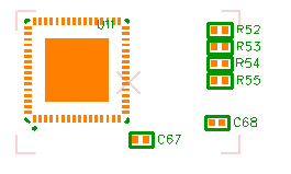
To create a group, select objects, and go to "Edit \ Group" from the main menu. To ungroup objects, select any object of the group, and go to "Edit \ Ungroup" from the main menu. It is also possible to group and ungroup objects from the object right-click submenu.
3.5.13. Pad (single)
A separate pad in DipTrace (which placed directly in the PCB Layout) behaves like a pattern with a single pad. Select "Objects \ Place Pad" from the main menu or press  button on the Elements toolbar, then left-click on the design area to place a pad.
Change default pad shape and size on the Place Pad panel (Properties tab) on the Design Manager (visible only when Place Pad tool is active).
Notice that you can hide a pad in any signal/plane layer. Right-click on the pad, and select Hide Pad Ring in Layer. Blind/buried pads are possible. Right-click on the pad to display its submenu, and select Pad Layers from the submenu.
To specify custom mask and paste settings, right-click on the pad, and select Mask / Paste Settings.
If you need to setup default pad properties for entire pattern, right-click on the pattern, and select Pad Properties from the pattern submenu.
If you need to customize certain pad of the pattern, right-click it, and select Pad Properties from the pad submenu.
3.5.14. Mounting hole
A mounting hole is a pattern with a single mounting hole. The mounting hole has only two parameters: the diameter of the hole and diameter of the keepout area around it (Outer Diameter).
To place a mounting hole, select "Objects \ Place Mounting Hole" from the main menu or press  button on the Elements toolbar. Change default mounting hole parameters in the Properties tab on the Design Manager (visible only when Place Mounting Hole tool is active).
To change the parameters of the mounting hole on the design area, right-click it, and select Properties from the submenu.
3.5.15. Fiducial
A fiducial is a pattern that consists of a single fiducial. Fiducial has only two parameters: the diameter of the exposed copper and diameter of the keepout area around it.
To place a fiducial, select "Objects/ Place Fiducial " from the main menu or press  button on the Elements toolbar. Change default fiducial parameters in the Properties tab on the Design Manager (visible only when Place Fiducial tool is active).
To change the parameters of the fiducial on the design area, right-click it, and select Properties from the submenu. In the pop-up dialog you can adjust fiducial position by setting X and Y coordinates and edit diameter of copper and keepout area.
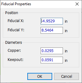
You can choose to Show or Hide fiducials of the components containing them in the current project by selecting the respective option for Component Fiducials item in View menu.
3.5.16. Planar Inductor
A planar inductor is a pattern that consists of copper windings. Designing planar inductors involves careful consideration of the trace width, spacing, and layer stacking to achieve the desired inductance and performance.
To create and place a Planar Inductor, select "Objects/ Place Planar Inductor" from the main menu. Alternatively, open the Planar Inductors tab in the PCB Calculator dialog.
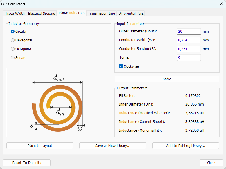
Choose Inductor Geometry, set Input Parameters: enter the Outer Diameter, Conductor Width and Spacing and the number of Turns. Press the Solve button for DipTrace to calculate the resulting Fill Factor, Inner Diameter and Inductance values.
Press Place to Layout to place the Planar Inductor directly to your design.
To save the Planar Inductor pattern for future use press Save as New Library or Add to Existing Library.
Press Reset to Defaults to revert to default values.
3.5.17. Dimensions
You can place four types of dimensions (horizontal, vertical, free, radius) and the pointer (it displays the point coordinates or custom text).
Dimension or pointer is attached to the object's key point. It automatically recalculates when you edit the object.
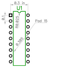
To place a dimension, select "Objects \ Place Dimension \ <Dimension Type>" from the main menu or press on the Elements toolbar, and select a type of dimension, then click on the first point (key points are highlighted) on the design area, and click on the second point (if necessary), then choose the dimension's position.
Right-click on a dimension, and select Properties from the submenu to disconnect or connect dimension from/to the key points, change/display units, and access other settings.
3.5.18. Search layout objects
To search layout, select "Edit \ Find in Layout" from the main menu or press Ctrl+F hotkeys.
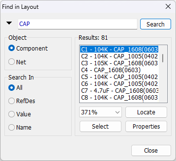
In the pop-up dialog box, select the object type (Component or Net) and the search criterion (All, RefDes, Value or Name). Then enter the full or partial search term and press Enter or click Search.
In the Results list, double-click an object or click Locate to highlight and center it in the design area.
To select objects, choose one or more entries in the Results list and click Select.
For direct editing, click Properties to open the object’s Properties dialog.
The Search dialog does not need to be closed while working with the layout. It can be minimized by clicking the arrow in the upper-left corner.
3.6. Editing objects
3.6.1. Selecting objects
Select objects before editing or removing them. DipTrace has several ways to select objects or to edit existing selection:
1. Clicking. Use the left mouse button to select an object and the right mouse button to open the object's submenu.
Notice that you can select different overlaying objects by clicking several times on the same spot.
2. Box selection. In the Default mode hold down the left mouse button on an empty place, and move the mouse to draw a selection box. All objects inside this box will become selected when you release the mouse button.
To invert object selection, press Ctrl key, and select objects. To add objects to selection, use the Shift key.
If you try to select one object from a group, the entire group becomes selected.
To select all objects, go to "Edit \ Select All" from the main menu or Ctrl+A hotkeys.
3. Edit Selection. This dialog box allows the user to select objects by type/layer. There are several selection modes: new selection, add to selection, remove from selection, keep selected. Go to "Edit \ Edit Selection" from the main menu.
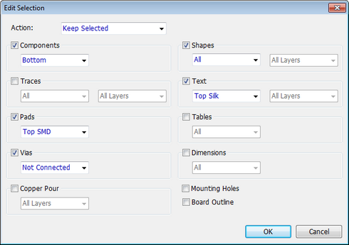
In the pop-up dialog box select objects and one of the modes:
1. New Selection – deselect all objects selected on the design area and create a new selection based on your choice;
2. Add to Selection – add specified objects to existing selection;
3. Remove from Selection – remove specified object/s from existing selection;
4. Keep Selected – deselect all selected objects, which do not correspond to specified parameters. This mode allows the user to select objects by type and area. Use box selection and Ctrl button to define an area, then use Keep Selected mode which will deselect all unspecified objects.
3.6.2. Cross Selection
DipTrace features Cross Selection and Cross Highlight between the Schematic and PCB, meaning that when objects (components, nets and pins) are selected or highlighted in the Schematic Capture, they are simultaneously selected/ highlighted in the PCB and vice versa.
To enable this feature, go to Edit/ Cross Selection in the main menu and mark Enable Cross Selection in the pop-up dialog.
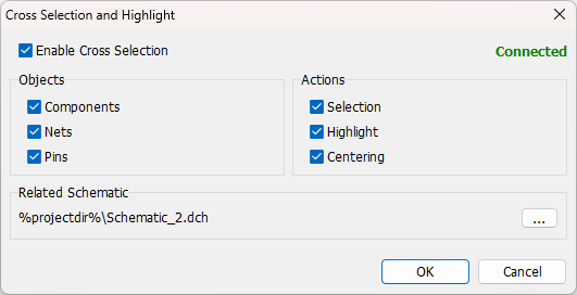
You can choose which objects will be selected or highlighted, and which actions will be synchronized between both modules when using this function.
Make sure related schematic is assigned to the PCB to use this feature. Press  to assign related schematic.
3.6.3. General functions
There are the following general editing functions: Delete, Cut, Copy and Paste.
Select objects first before applying these functions, then select the corresponding action from Edit main menu item or use the hotkeys: Cut (Ctrl+X), Copy (Ctrl+C), Paste (Ctrl+V) and Delete (Del). You can copy objects between two DipTrace instances.
To create a matrix, based on selected objects, select "Edit \ Copy Matrix" from the main menu, define the number of columns and rows, column and row spacings, and press OK.
3.6.4. Undo/Redo function
To cancel the last editing step and return to the previous design, select "Edit \ Undo" from the main menu or press  button on the Standard toolbar.
It is possible to recover canceled steps. Choose "Edit \ Redo" from the main menu or press  on the Standard toolbar. If you edit layout after using Undo tool, the Redo tool becomes inactive.
You can select whether to consider Zoom a separate editing step or not, using Undo/ Redo Zoom item of Edit menu.
3.6.5. Undo/Redo Zoom
You can select whether to consider Zoom a separate editing step or not, by choosing from the following options:
Change if action not visible. If the editing step being canceled does not belong to the currently visible area of the design field, the first Undo command will return the view to the previous scale to make the location visible again; the second Undo command will cancel the action. If the location is visible on the design area, the first Undo command will cancel the action.
Change Always. The change of the scale is always considered as a separate editing step. Undo command returns the view to the previous scale.
Do Not Change. Undo command cancels the last editing without changing the scale.
3.6.6. Move/Rotate objects
To change the position of design object/s, select them, and drag to a new position. You can also use the Arrow keys. Hold Shift for orthogonal moving.
Connected trace segments change while moving the component.
To rotate objects counter-clockwise, select them, and press R hotkey (by default) or select "Edit \ Rotate" from the main menu.
PCB Layout allows the user to rotate selected object/s to any angle. Right-click on the component, shape or copper pour, and select Define Angle or Free Rotate from the submenu.
Define angle item allows the designer to select 30, 45 degrees or specify a custom angle. Free Rotate is used to rotate objects visually with the mouse. Left-click when done.
To rotate the selected objects with a single center point, select "Edit \ Rotate Group" from the main menu.
To flip the selected objects, go to "Edit \ Flip Group" in the main menu. DipTrace will mirror vertically or horizontally both the location and angle of the selected objects.
3.6.7. Aligning objects
Select objects on the design area, then go to "Edit \ Align Objects" from the main menu, or right-click on one of the objects and select Align Objects from the submenu.
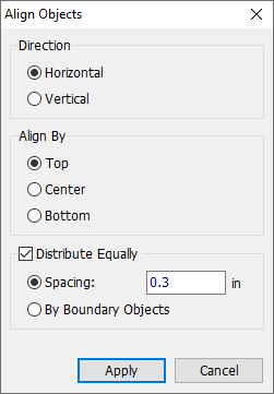
Select the alignment direction, then select how to align objects in the row or column (left, center or right) and set distribution settings by objects' boundaries or equally with a custom spacing.
You can group multiple objects into one so they will stay together if they are aligned or distributed.
At least two objects (or groups of objects) have to be selected for the Align tool to become available because the alignment is relative.
3.6.8. Radial Placement
DipTrace allows for radial placement of components, individual pads, mounting holes, vias and fiducials. Select one or several objects on the design area, then go to "Edit\ Radial Placement" from the main menu or right-click on one of them and select Radial Placement from the submenu.
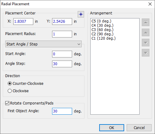
You can enter the coordinates of the point that will be used as placement center or press  button and set it with the mouse pointer in the design area.
Enter Placement Radius - the distance between the placement center and the origin point of the object.
Use the drop-down to select how you want the objects to be distributed: based on Start Angle and Step or Start and End Angles.
Define placement Direction - clockwise or counterclockwise.
Mark Rotate Components/ Pads and set the First Object Angle, if you want the objects to be rotated to a certain angle when placed radially.
In the Arrangement section use arrow buttons to change the order of the objects in the array.
3.6.9. Lock/Unlock objects
PCB Layout has two ways to lock objects:
1. Lock Selected. To lock selected objects (prevent moving, editing, etc.) select objects, right-click on one of them, and choose Lock Selected from the submenu, "Edit \ Lock Selected" from the main menu or Ctrl+L hotkeys. To unlock selected objects, choose "Edit \ Unlock Selected" from the main menu or Unlock Selected item from the object submenu. Locked objects highlight with lower contrast.
2. Locking components by side. This feature allows the designer to lock components on the Top or Bottom side of the board. Select "Edit \ Lock Components \ <Board Side>" from the main menu to lock or unlock components on the corresponding PCB side.
3.7. Placement
3.7.1. Arrangement
Once schematic is converted to PCB, a layout usually seems chaotic. The Arrange Components feature positions all components into the box inside or outside the board outline depending on the settings.
Placing components outside the board outline is useful before placing components by the list.
Change default clearances between the components in the Placement Setup dialog box, custom component clearance – in the Component Properties dialog box.
To launch the arrangement, select "Placement \ Arrange Components" from the main menu or press  button on the Placement toolbar.
Notice that Auto-Placement and Arranging Components are different features.
3.7.2. Placement by List
Select "Placement \ Placement by List" from the main menu:
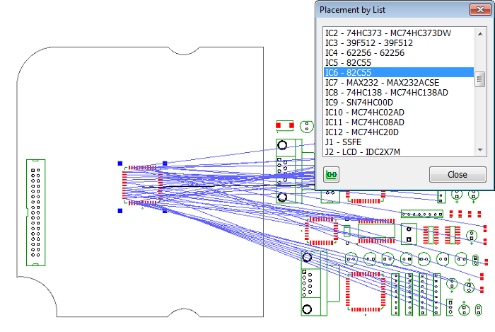
Select component from the list in the pop-up dialog box, and left-click to place it inside the board outline. Placed components disappear from the list.
Notice that only nets connected to selected component are shown.
3.7.3. Place Selected by List
DipTrace allows selecting components in the Schematic and placing them by list in the PCB Layout. To use this tool, make sure that related schematic is assigned and Cross Selection is enabled (go to Edit/ Cross Selection in the main menu and mark Enable Cross Selection in the pop-up dialog).
Components selected on the schematic are simultaneously selected on the PCB. Go to Placement/ Place Selected by List in the main menu, the components selected on the schematic will be shown as a list in a separate window. Now you can drag the components directly from the list to place the on your layout.
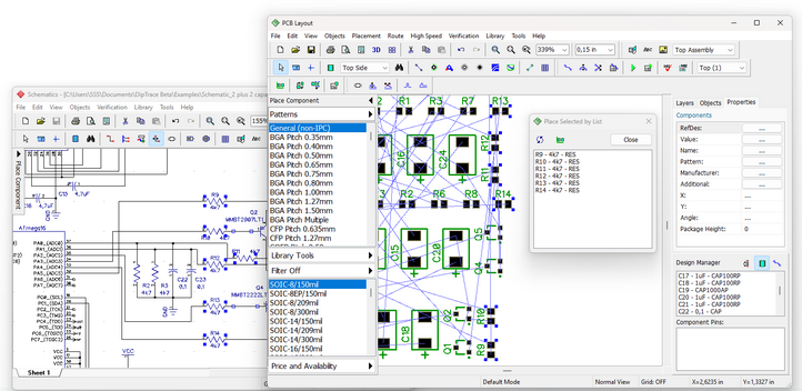
Once placed, select the next batch of components on the Schematic and press  in the Place Components by List window to update the list.
3.7.4. Auto-placement
Auto-placement feature optimizes component layout by connections' lengths.
We recommend using a combination of automatic and manual placement (Placement by List) for complex designs. Place all primary components (chips, connectors, etc.) manually, and lock them ("right-click \ Lock Selected"), then auto-place resistors, capacitors, small chips, etc. This saves your time and optimizes the total trace length and number of vias required.
See Placement by List to discover more.
To define auto-placement parameters, use the Placement Setup dialog box ("Placement \ Placement Setup" from the main menu) and Component Properties for components with a custom clearances.
Select "Placement \ Run Auto-placement" or press  button on the Placement toolbar.
It is possible to auto-place selected components only (for example, some logical block, etc.) – go to "Placement \ Auto-place Selected" from the main menu or press  button on the Placement toolbar. Regular placement parameters apply.
3.7.5. Placement setup
Placement Setup dialog box allows the designer to define settings for arrangement and auto-placement features. Select "Placement \ Placement Setup" from the main menu or press  button on the Placement toolbar:
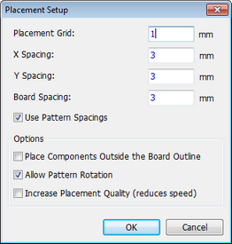
Placement Grid is used for auto-placement and arrangement. This value does not mean accuracy because placement algorithm uses combined grid and shape methods to make accurate spacings.
The X, Y, and Board spacing mean horizontal/vertical spacing between different components and the minimal distance from components to the board outline.
Use Pattern Spacings means using custom pattern clearances. See the Placement tab in the Component Properties dialog box.
Place Components Outside the Board Outline can be used to place components right next to the board outline before placing them by the list.
Increase Placement Quality is the optimization for each placement step. This increases the quality, but dramatically reduces the speed (use with caution).
3.8. Routing
3.8.1. Routing steps
We describe a typical working sequence in DipTrace PCB Layout:
1. When you open a schematic file in the PCB Layout, the program suggests to use schematic rules or load rules from a previous layout project (layers, DRC parameters, net classes, and via styles). If you have selected to load rules, you can skip layers/via styles/net classes/DRC configuring steps.
2. Draw the board outline or import it from mechanical CAD and arrange components (outside the board outline, see Placement Setup)
3. Place components on the board (see Placement by list). Auto-placement for non-critical components.
4. Configure layers ("Route \ Layer Setup" from the main menu).
5. Configure via styles ("Route \ Via Styles" from the main menu).
6. Configure net classes ("Route \ Net Classes" from the main menu).
7. Route the board: automatically or in the manual mode.
If you design a simple board with two layers, single trace width and single via style is probably enough. In this case skip steps 4 through 6. Use the Routing Setup dialog box to quickly configure the basic settings.
3.8.2. Adding ratlines
There are several ways to add ratlines (create new nets) in DipTrace PCB Layout:
1. To connect two pads with the mouse, select "Objects \ Place Ratline" from the main menu or press button on Objects toolbar. Then left-click on the first pad, and move the mouse to the second pad, left-click it. DipTrace creates a new net (connection line appears). Right-click if you want to cancel connection while creating it and switch to Default mode. Connect as many pads as you need.
2. To connect a pad to existing net, right click on the pad, select Add to Net, then choose Select from List, select net, and click OK. Ratline connects the current pad with the nearest pad of selected net. You can also connect all selected pads or vias at a time. Edit Selection feature allows the user to manage the selection of pads/vias before connecting them.
3. Connection Manager, select "Route \ Connection Manager" from the main menu. Here you can add or delete pads to all nets as well as add new nets to the design.
Locking the net structure prevents adding/removing ratlines with all methods listed above. In this case, the ratline disappears only if you route it. To lock the net structure, go to "Route \ Lock Net Structure" from the main menu.
3.8.3. Connection Manager
Go to "Route \ Connection Manager" from the main menu.
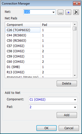
In this dialog box, you can select a net and add or delete pads to/from this net.
Rename net by pressing the button, or delete it with the  button. To add a new net, press
  .
.
To delete pad, select it in the table, and press Delete button.
To add pad, select component and pad of this pattern, and press Add button.
3.8.4. Routing setup
To change basic routing parameters, select "Route \ Routing Setup" from the main menu or press  on the Route toolbar.
|
|
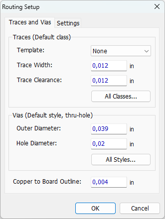
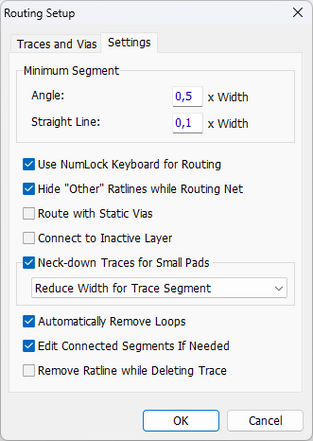
In this dialog box you can change the following parameters, sorted by two tabs:
Traces and Vias
Trace width and clearance for default net class (enough for the majority of simple layouts). If you need more net classes/rules for your layout, click All Classes button to configure new net classes.
Outer diameter and hole diameter for default via style (always default through-hole vias). If you need more via styles or blind/buried vias, click the Via Styles button.
Copper to Board Outline. This clearance applies to both the Board Outline and Board Cutout, as well as to the autorouter.
Settings
Minimum segments are used while editing traces to remove very small segments and make straight lines or angles. Try different values and edit some tracks on the design area to select the best value for you. However, very few people need this kind of customization, since default values work for almost any situation.
Use NumLock Keyboard for Routing – enable manual routing of 90/45 segments using Num Keypad.
Hide ''Other'' Ratlines while routing net. If you want to display all ratlines of the layout while routing a certain net, uncheck this parameter or select "View \ Ratlines \ Routed Net Only" from the main menu.
Automatically Remove Loops – automatically remove looped ("bow tie") trace segments when completing a trace. This option is not applied when there are T-junction, since multiple valid connection paths may exist.
Neck-down Traces for Small Pads: This option allows you to adjust trace width when routing to small pads. You can choose between two settings:
Reduce Width for Trace Segment (default): DipTrace automatically reduces the width of the first trace segment to match the pad size when the trace is wider than the pad.
Reduce Width for Pad Only: This option reduces the trace width only at the point where the trace connects to the pad, keeping the rest of the trace at its original width.
Route with Static Vias – activate this option if you want static vias to be placed instead of trace vias during routing.
Connect to inactive layer – highlight traces in all layers when you hover over them in the Manual Routing mode. This feature is often used with Highlight only current net option because in this case, the software highlights pads and traces of the net being routed regardless of the PCB layer. You do not need to change the layer – a via appears automatically.
Remove Ratline while Deleting Trace – remove a ratline together with a trace being deleted.
3.8.5. Interactive Routing Setup
Select Route / Interactive Routing from the main menu to open the Interactive Routing Setup dialog box. Alternatively, press .png) button in the Interactive section of the manual Routing Toolbar or Edit Objects panel. The dialog contains three tabs for configuring interactive routing behavior during Routing, Trace&Via Editing and Object Editing.
button in the Interactive section of the manual Routing Toolbar or Edit Objects panel. The dialog contains three tabs for configuring interactive routing behavior during Routing, Trace&Via Editing and Object Editing.
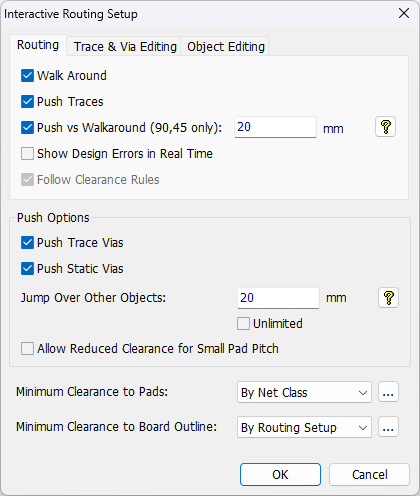
Routing Tab
Use this tab to configure Walk Around, Push Traces, and Push vs Walk Around options that will be applied when creating new traces. Push vs Walk Around allows defining the balance between push-based routing through the shortest path and walk around routing with increased trace length to reduce trace pushing.
Enable Show Design Errors in Real Time to highlight routing and clearance violations while routing.
When both Walk Around and Push Traces options are disabled, enabling Follow Clearance Rules prevents clearance violations while routing nets.
Configure Push Options for vias: enable Push Trace Vias and/or Push Static Vias if you want DipTrace to automatically relocate vias while routing. If these options are not selected, vias will be treated as obstacles.
Jump over other objects: traces and vias can automatically jump over pads, traces and other objects. Adjust the distance at which the software searches for suitable placements. Higher values and enabling the Unlimited option increase rerouting flexibility, but may affect performance.
Allow Reduced Clearance for Small Pad Pitch option is helpful when working with fine-pitched packages. This option adjusts the clearance based on the current trace width and pad pitch, even if it violates net-class rules. However, clearance cannot be smaller than the value set in Design Rules.
Choose whether Minimum Clearance to Pads and Board Outline is defined By Net Class, Routing Setup or By Design Rules. Press for direct access to the Net Class, Routing Setup and Design Rules dialogs.
Trace & Via Editing Tab
This tab allows configuring Walk Around and Push options for Editing of Traces and Vias. Most options are similar to those available on the Routing tab. However, this tab also includes additional options that improve trace editing flexibility.
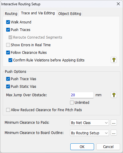
Reroute Connected Segments – when Walk Around mode is disabled, and traces are edited in Push Traces mode, this option allows connected segments of the edited trace to be automatically rerouted when they block further editing. This allows more flexible trace modification while preserving connectivity and routing constraints.
Confirm Rule Violations before Applying Edits – available when Follow Clearance Rules is enabled. When selected, a confirmation dialog is displayed before applying edits that would violate routing rules. When cleared, edits are applied immediately and any violations are indicated on the board. Real-time editing is not affected.
Object Editing Tab
This tab allows configuring interactive routing behavior when editing objects. Most options are similar to those available on the Routing and Trace & Via Editing tabs.
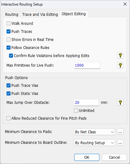
A condensed version of the Trace & Via Editing and Object Editing options is displayed in the panel on the left when editing traces, vias, or other objects.
3.8.6. Trace templates
To set up trace templates (width and clearance) select "Route \ Trace Templates" from the main menu.
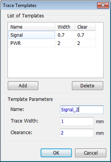
In the pop-up dialog box add, delete, and change trace templates.
Trace templates appear in the net submenu when you select to change the segment/trace/net width. Trace templates are also available in the Net Properties and Routing Setup dialog boxes.
3.8.7. Routing traces
DipTrace features manual and automatic routing modes.
|
To create a trace manually, select Route/ Manual Routing/ Add Trace from the main menu, press
To begin trace routing, anchor a starting point by left-clicking on a pad, via, trace or an empty spot, draw a trace and connect it to the end point by left-clicking on a conducting circuit element (pad, via, trace). To finish a trace on an empty spot, just press Enter or right-click, and select Enter from the submenu. To cancel the trace, use Esc key or right-click, and select Cancel from the submenu. To return to default mode, right-click on a blank spot, press
Routing parameters can be managed on the Routing panel.
Interactive features ensure fast and error-free routing.
Walk Around. This option automatically guides traces around pads, existing traces, and other board objects while maintaining the selected segment’s shape and characteristics. It can be used together with the Push Traces option for more efficient trace handling. Enable/ disable this option on the Routing panel or with "Y" hotkey.
Push traces. This function allows the user to move traces and vias around a PCB without manually rerouting surrounding traces, simply push a new track through already laid structures. Enable/ disable this option on the Routing panel or with "I" hotkey.
Show Errors. If this box is checked, all routing errors will be highlighted with red circles in real time, when a trace is being routed. By contrast, Real-time DRC, when enabled, shows errors immediately after the trace routing process is finished.
Follow rules (F hotkey). With this option activated, the software will not allow any violations of design rules when routing existing nets.
Press
|
Routing Mode. Select the required option or use M hotkey to choose between Orthogonal, 90/45 Lines, 90/Arcs, customized or All Segments routing mode.
All Segments mode allows the user to choose from all available types of trace segments. Other modes imply using segments of a certain type only. Use S hotkey to toggle between the segment types.
My Routing Mode enables creating a customized set of segments for quick access during the routing process. Press button to open the list of available options and select the required ones. Press OK.
Current Segment. This item serves to change the current trace segment using S hotkey or by selecting the necessary option from the list that appears when left-clicking on the current segment image. The set of available segment types depends on the selected Routing Mode. DipTrace allows drawing orthogonal polylines (90 Horz > Vert, 90 Vert > Horz), polylines with determined vertex angle (90 deg. line > 45 deg. line; 45 deg. line > 90 deg. line) as well as rounded lines (90 deg. line > arc; arc > 90 deg. line) and 3-point arcs. If free line or curve option is selected, the angles of a polyline or the shape of a curve can be defined by the user.
Fix Single Line. This option is applicable to polylines and rounded lines. With this item selected (checkbox on Routing panel or D hotkey), a left click will fix only the first angle-forming segment, placed before the vertex point, leaving the second one in placement mode.
Net Class. Use a drop-down list or C hotkey to choose a net class for a new net created during routing process.
Please note that changing a net class on this panel does not change the class of an existing net. To change the net class of an existing net, open the Net Classes (link to 6.4) dialog-box and change it prior to routing.
Segment Width. The width of the current trace segment is displayed here. Select By class to use the value defined by the Net Class properties or customize this parameter for the current and following segments by typing in the required value. Use W hotkey for a quick access to the list of options for defining the width of the current segment: Net Class, Template, Custom.
Segment Layer. Use the drop-down list on the Routing panel, L hotkey or a layer number from 1 through 9 to change the current routing layer. Additionally, you can use T and B hotkeys to switch to Top and Bottom layer respectively. Trace vias appear automatically.
Via Style. Use a drop-down list or V hotkey to select a via style that will be applied to the vias that appear, if you change the layer when routing a trace. Auto means that DipTrace selects an optimal via style, depending on the situation.
Via preview. Mark the checkbox or use E hotkey to enable/disable this option. When activated, a via that will be placed when changing the trace layer is shown at the tip of the line while routing.
Angle Step. This item is activated when curve or free line is selected as Current Segment. Use drop-down menu or A hotkey to change the angle step to free, 15, 30 or 45 degrees.
Highlight Net. Here you can chose to highlight pads of all nets or only the pads of the current net while drawing a trace. Select the preferred mode or use H hotkey to toggle between the options. Current Net mode is highly recommendable, when Follow rules option is disabled, because it also ensures error-free PCB design by highlighting only those pads and traces that belong to the current net when you hover over them with the mouse pointer in the Manual Routing mode; other traces and pads are basically ignored, making connection to them impossible.
Undo button, same as U or Backspace hotkey, allows undoing the last trace segment.
You can use P hotkey to pause routing. Once the routing is paused, you can edit your layout and then resume trace routing by hitting P hotkey again.
All the routing parameters are duplicated in and can be adjusted from the right-click submenu when routing a trace.
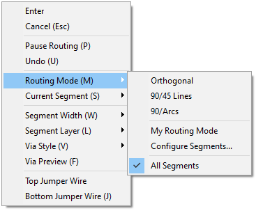
Note that if you connect a trace to a pad or a trace belonging to another net the software will display a menu for you to choose what you would like to do: merge the nets; move the pad from its original net to the currently routed net; continue or cancel routing.
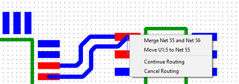
You can use Num Keypad for manual routing of 90/45 segments. First, activate Numpad with NumLock key. Make sure that Use NumLock Keyboard for Routing option is enabled in the Settings tab of Routing Setup dialog (Route/ Routing Setup). Switch on Manual Route mode and left-click in the starting point to begin routing a trace. Use Num keys for routing in the following directions:
You can finish routing a trace with Numpad by pressing Enter key. It is possible to switch to routing with the mouse and back to Num keys at any moment.
Routing with Numpad is done only with 45/90 segments, irrespective of the current Routing Mode and Segment type.
3.8.8. Editing traces
Editing traces – moving, adding nodes, changing trace width and layer.
There are two modes of moving traces:
1) Edit existing trace respecting 90- and 45-degree angles. This mode is activated automatically when you try to edit some trace in the Default mode. To enable edit mode manually, go to "Route \ Manual Routing \ Edit Traces" from the main menu or press button on the Route toolbar. This mode allows the user to move trace segments with 90- and 45-degree angles and to smooth 90-degree "sharp" angles with two angles and a segment, like on the picture below:
2) Free edit trace. To enable this mode, select "Route \ Manual Routing \ Free Edit Traces" from the main menu or press button on the Route toolbar. This mode allows for moving trace segments and nodes in any direction anywhere on the design area.
To add a node to a trace segment, hover over it with the mouse, and press N hotkey or right-click, and select Add Node from the submenu. New nodes remain on the trace for several steps until they are automatically removed if unused.
To perform any action with a trace segment, you need to select it first. DipTrace allows the user to select several trace segments at a time with the left mouse clicks (hold Ctrl key and add/remove segments to/from the selection, or use the box selection and Shift key).
All selected segments are displayed by the dotted lines; the Properties tab shows their properties (Ctrl+2 to show/hide the Design Manager).
Four segments selected
Press W hotkey or enter a new value into the Segment Width field on the Properties tab. You can also change the trace width. Select the width from the trace templates or set a new value. To change segment layer, select layer from Segment Layer drop-down list on the Properties tab.
Properties tab includes major net properties: change net class, color, route mode, same as in the right-click submenu.
To delete a segment, right-click it, and select Delete from the submenu.
To unroute segment, trace or net, right-click it, and select Unroute <item> from the submenu.
Edit Traces Panel
The Edit Traces panel appears automatically once Edit Traces mode is activated. It provides quick access to interactive routing options and allows the designer to quickly adjust routing behavior without opening additional dialog boxes.
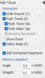
Walk Around – route around existing objects.
Push Traces – automatically move existing traces when routing a new trace through occupied areas.
Push Trace Vias – allow moving trace vias during push routing.
Push Static Vias – allow moving static vias during push routing.
Reroute Connected Segments – when Walk Around mode is disabled, activating this option allows connected segments of the edited trace to be automatically rerouted when they prevent further editing. This provides more flexible trace modification while preserving connectivity and routing constraints.
Show Errors – display routing and design rule violations directly on the design area.
Follow Rules – apply current design rules and routing constraints during interactive routing.
Edit Connected Segments – Allows segments connected to the edited trace segment to be adjusted automatically during editing, preserving trace continuity and reducing the need for manual modifications.
Minimum Segment – Defines the minimum length of segments that may be created during trace editing, relative to the trace width. Separate limits can be specified for angled and straight segments to prevent the creation of very short routing artifacts.
Interactive Routing Setup – press to open the Interactive Routing Setup dialog box for detailed configuration of the routing parameters.
3.8.9. Routing differential pairs
DipTrace allows the user to route two tracks simultaneously or one by one.
Double-track routing
Routing a differential pair is very similar to routing regular nets. Press button on the Route toolbar, or use Tilde sign (~) hotkey, then left-click on any of the differential pair pads, and start drawing the traces. Two tracks of the pair with specified gap appear on the design area simultaneously.
Left-click on the key point of the track to create a node, use Routing panel on the left for any on-the-go customizations. Please refer to Routing Traces topic for manual routing basics, which are also applicable to differential pairs.
Single-track routing
Sometimes you need to separately route each track of a pair to succeed. When in the differential pair manual routing mode, right-click, and select Route Single Trace from the submenu, then continue drawing a track to its pad.
In order to change the track being routed, select Change Control Trace from the right-click submenu.
If you want to return to pair routing, select Route Pair from the right-click submenu. When one of the pair tracks is routed, DipTrace automatically switches to the unrouted net.
Currently, automatic differential pair routing is not possible in the DipTrace, but differential pairs can be routed using external software SPECCTRA/ELECTRA via DipTrace DSN/SES interface.
3.8.10. Editing differential pairs
Editing differential pair traces – moving tracks, adding nodes, changing the width and layer of the tracks.
Editing of routed differential pairs is quite similar to editing single tracks (if you are new to the software, read that topic first) the only difference is that with differential pairs you can edit two tracks simultaneously or each track separately from the other.
Editing as a pair
Go to "Route \ Manual Routing \ Edit Traces" from the main menu, or press button on the Route toolbar. This is a regular track edit mode that allows the user to move two tracks of a differential pair simultaneously respecting 90- and 45-degree angles. The differential pair, in this case, behaves just like a single trace. Select tool to simultaneously edit two tracks of the pair without any constraints.
To add a node to the traces, move the mouse pointer over the trace segment, and press N hotkey or right-click, and select Add Node from the submenu. New nodes remain on the traces for several steps until they will be automatically removed if unused.
In order to change the differential pair name, color, unroute any part of the pair, change layer of the segment, trace, or entire differential pair, just right-click on the trace, and select the corresponding item from the drop-down list.
Basic differential pair properties are available on the Properties tab of the Design Manager when a differential pair is selected.
Single-trace editing mode
For a single track editing, go to "High Speed \ Differential Pair Tools", then select Edit Single Trace for editing a single trace respecting 90-and 45-degree angles or select Free editing of Single Trace.
You can also use the and buttons to launch the respective single-trace editing modes.
Neck differential pair
Go to Net Classes dialog box ("Route \ Net Classes" from the main menu), select the differential pair net class, and press Neck Parameters button. Enter the trace width and gap between the traces. Max Neck Length parameter allows the user to define the maximum length of the necked trace segment. If it is longer than this value, the DRC drops an error.
When routing differential pair on the design area, right-click, and select Neck-down Segment from the submenu, or use W hotkey.
To return to normal width, select Return to Regular Width from the right-click submenu.
Phase Tuning
Net Class settings control a maximum uncoupled length of a differential pair, length tolerance for the two tracks of a pair, dynamic phase tolerance and the maximum length of a segment with dynamic phase tolerance violation. DRC verifies the circuit board according to these parameters. If the DRC reports a phase shift (dynamic phase tolerance violation), select the Phase Tune tool to find the problem and ensure that the timing on the differential pair signals is correct.
Press button on the High Speed toolbar, or select "High Speed \ Differential Pair Tools \ Phase Tune" from the main menu. With the Phase Tune for Differential Pairs tool, you can hover over the differential pair trace, and check if there is a phase delay or hurry on a particular trace segment counting from both ends of the trace in forward and backward directions.
Left-click on the segment, and drag and drop to create a meander. Meanders are created one at a time. This reduces the phase timing difference between the two tracks of a differential pair. You can control a current phase shift value in the Phase Tune for Differential Pairs dialog box.
DipTrace considers a signal delay on the pads and via height determined by the layer stack when calculating trace length and signal phase.
3.8.11. Editing objects
Edit Objects Panel
The Edit Objects panel appears automatically when selecting traces, vias, pads, or other routing-related objects during interactive routing. It provides quick access to interactive routing options and allows the designer to quickly adjust routing behavior without opening additional dialog boxes.
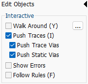
Walk Around – route around existing objects.
Push Traces – automatically move existing traces when routing a new trace through occupied areas.
Push Trace Vias – allow moving trace vias during push routing.
Push Static Vias – allow moving static vias during push routing.
Show Errors – display routing and design rule violations directly on the design area.
Follow Rules – apply current design rules and routing constraints during interactive routing.
Press button to open the Interactive Routing Setup dialog box for detailed configuration of the interactive routing parameters.
3.8.12. Measuring trace length
There are three ways to measure traces:
1. Using the trace hint. When you hover over some trace, a hint pops up. For it to include the information about the trace length, enable Add Object Details item in the View/ Display Hint submenu. The trace length is shown in the following format: "Length (start point - end point) = XX.XXX".
2. Selecting the traces. Select the traces that you want to measure, right-click on one of them, and choose Show Trace Length from the submenu. The length value appears for each trace (near the pads). The value changes in real-time when you edit traces, this allows for precise length control on the go.
3. Length-Matching Tool. A special tool for comparing trace lengths and matching them by using meanders (extensively used when routing high-speed buses). Find out more in the next topic.
Notice that pad signal delay and via height, defined by the layer stack, are added to the total length of traces being measured.
3.8.13. Length matching
DipTrace PCB Layout allows the designer to compare lengths of selected nets automatically and correct the routing using an auto-updated length comparison list. Traces can be compared against each other with a custom tolerance or against a Fixed Length value.
We recommend creating a separate net class and checking the Length Matching by Class box in the Net Classes dialog box if matching tracks of a bus.
Otherwise, you can select "High Speed \ Length Matching" from the main menu or right-click on the track, and select Length Matching, then Open Length Matching from the submenu to set up the constraints, add nets, and create a DRC rule for verification.
Press Add Net/Pads to select a net and set the starting and ending pads. You can compare lengths of several traces against each other with a Tolerance value (just leave the Fixed Length field empty), or compare them against a target value (enter the Fixed Length parameter). In the latter case, a Tolerance value is automatically divided by two in order to show the ± tolerance above and below the Fixed Length.
Press Create New Rule to save current length-match settings as a DRC rule.Otherwise, the DRC will not verify lengths of the traces.
Notice that you can left-click on several traces with a Ctrl key, and select "Length Matching \ Compare Selected Nets Only" from the submenu to launch the Length Matching tool for selected nets only.
Use the drop-down list in the Rule section to switch between different length-matching rules of the current circuit board. Press the button in the Rule section to rename or delete rules.
Press a corresponding button to replace net or swap its starting and ending pads. Press to delete net from the list.
DipTrace considers layer stack and pad signal delay when calculating trace lengths. Press the corresponding button at the top of the dialog box to toggle these options.
Meanders
Meander is the most efficient way to make traces longer and length-match them. Press on the High Speed toolbar or select "High Speed \ Add Meander" from the main menu, then left-click on the trace, and drag and drop to create a meander. Meanders are created one at a time. The software helps to create meanders of the same size.
To edit meanders, press button, and drag and drop meander's vertices. To push one or several meanders along the trace, left-click on the trace segment opposite the preferred direction, and drag and drop several meanders.
Notice that you can also use the Add Meander mode ( button) to edit meanders.
By default, the gap between the meanders is defined by the net class clearance. To set custom meander gap, right-click on the trace, and select Meander Gap from the submenu. In the pop-up dialog box, check Value box, enter new gap, and press OK.
3.8.14. Fanout
The Fanout feature allows the designer to automatically create vias for SMD patterns (SOIC/QUAD, and BGA footprints), nets, and pads. Fanout is a very convenient tool when you need to connect SMD pads with internal PCB layers automatically.
Fanout pattern
To fanout a pattern, right-click it, and select Fanout from the submenu.
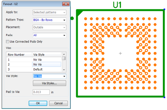
In the pop-up dialog box you can change the following parameters:
Pattern Type – select the pattern type: SOIC/QUAD, BGA - All Pads, and BGA - By Rows.
For example, the BGA - All Pads type allows the user to create vias of the same style for all pads of the pattern, BGA - By Rows enables separate via styles for each row of the BGA pattern, it also allows for rows without vias.
Placement – place vias outside, inside pattern or zig-zag. This option is active only for SOIC/QUAD patterns.
Pads – place vias for all pads or only for left/right/top/bottom line of the pads. This option is active only for SOIC/QUAD patterns.
Use Connected Pads Only – check this option if you need to create fanouts only for the pads connected to some nets.
Apply to – apply fanout for selected pattern, net or pad. You can not change this option because we clicked on the component pattern.
Fanout net or pad
To fanout a net, right-click on any pad of the net, select Fanout from the submenu, make sure that Net is selected in the Apply to field, and click OK. Fanouts appears for all pads of the net.
To fanout only selected pad, right-click on the pad, select Fanout from the submenu, select Pad in the Apply to field, and click OK.
3.8.15. Autorouting
DipTrace PCB Layout has two integrated autorouters:
1. High-speed shape-based autorouter suitable multi-layer SMD circuits.
2. Entry-level grid-based autorouter for simple hobby circuit boards with jumper wires.
Go to "Route \ Current Autorouter" from the main menu to select a current autorouter. Shape Router is selected by default.
Select "Route \ Run Autorouter" from the main menu, or press  button on Route toolbar, or Ctrl+F9 hotkeys to launch selected autorouter.
To change settings of current autorouter, select "Route \ Autorouter Setup" from the main menu or press  on the Route toolbar.
The errors may occur during automatic routing (depends on current routing settings), this is why the DRC (Design Rules Check) automatically verifies the circuit board right after autorouting. Go to "Route \ Current Autorouter \ Run DRC after Autorouting" from the main menu to turn this option ON/OFF.
To increase the routing speed, go to "Route \ Current Autorouter \ Redraw Traces while Autorouting" from the main menu, and uncheck this option.
Each net has an Auto-route Mode parameter in the Net Properties:
Ratlines – existing traces do not change while autorouter creates new traces based on current net structure (this mode is set by default);
Correct Traces – autorouter may correct existing traces and routes the circuit board based on current net connections;
Full – autorouter unroutes all existing traces and routes the circuit board based on current net connections;
Don't Route – do not route the net.
You can also route nets only of selected components, right-click on the component, and select Route Traces from the submenu.
Autorouting progress bar appears in the top-right corner of the design area.
3.8.15.1. Grid Router
3.8.15.1.1. Review
Grid Router is a grid-based autorouter with "rip-up-and-retry" technology. It's is suitable for simple projects. The speed of autorouting depends on the number of layers.
There are three basic autorouter steps: trace placement with "rip-up and retry" technology, trace optimization, and trace correction.
Autorouter has four modes: Quick (set by default), Normal, Good, and Best. To change the autorouter mode, select "Route \ Autorouter Setup" from the main menu or press button on the Route toolbar. Make sure that the Grid Router is selected as an active autorouter ("Route \ Current Autorouter \ Grid Router" from the main menu).
Advanced users can set up the Grid Router parameters manually.
3.8.15.1.2. Parameters
To change Grid Router parameters, select "Route \ Autorouter Setup" or press button on the Route toolbar. Make sure that Grid Router is selected ("Route \ Current Autorouter \ Grid Router" from the main menu).
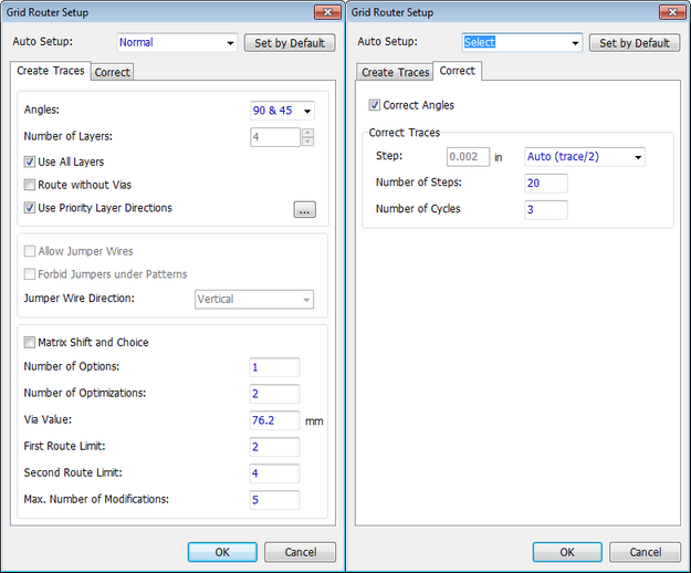
We recommend to set up the autorouter by selecting one of the modes (Auto Setup: Quick, Normal, Good, and Best).
Advanced setup for in-depth customization.
Tabs:
Create Traces
1. Angles – traces with 90-and 45-degree angles (default) or only 90-degree angles.
2. Number of Layers – set the number of signal layers available for the autorouter. Uncheck Use All Layers item, then set the number of PCB layers to 1, and the Grid Router draws all traces on the Bottom layer of the circuit board.
3. Use All Layers – check to allow the autorouter to draw traces on all PCB layers, uncheck to set the Number of Layers.
4. Route without Vias – the autorouter tries to route the circuit board without vias. We recommend using the Normal Auto Setup mode and raise the Number of Layers if autorouting fails.
5. Use Priority Layer Directions – use priority directions for traces on different signal layers. This feature allows the user to avoid parallel signals. Press to set up the priority trace directions for each layer.
6. Allow Jumper Wires – allow the autorouter to use jumper wires. We recommend using Normal Auto Setup mode for routing with jumper wires.
Notice that all jumper wire options are active only when routing the circuit board on a single layer (Use All Layers item is unchecked, and the Number of Layers set to 1).
7. Forbid jumpers under Patterns – check this item to forbid the Grid Router to draw traces under component footprints.
8. Jumper Wire Direction – select vertical or horizontal jumper wires.
9. Matrix Shift and Choice – enables the Grid Router to shift the routing grid to find the best variant.
10. Number of Options – the number of attempts for one grid shift variant.
11. Number of Optimizations – the number of trace optimizations.
12. Via Value – value of the via which is used to calculate the trace length, only for experienced users.
13. First Route Limit, Second Route Limit – the part of "rip-up-and-retry" technology to find traces. These limits set the maximum ratio of the trace length and "start-to-end-point" spacing. Only for experienced users.
14. Maximum Number of Modifications – the part of "rip-up-and-retry" technology to define the maximum number of trace reroutings.
Correct
15. Correct Angles – delete sharp angles.
16. Correct Traces – set the correction step, number of steps per attempt and number of correction cycles.
3.8.15.2. Shape Router
3.8.15.2.1. Review
DipTrace has an integrated world-class high-speed shape-based autorouter capable of processing complex multi-layer SMT layouts as well as simple hobby-level circuit boards. The Shape Router algorithm is based on adaptive shape-based technology. The autorouter can create fanouts for nets and components, neck-down the traces and more.
You can define the routing strategy with Autorouter Setup or with a special DO-file (Electra/Specctra DO-file syntax).
Autorouter parameters are optimized for different kinds of boards, but you can change them if you need.
Notice that the Shape Router does not support jumper wires.
3.8.15.2.2. Parameters
To change the Shape Router parameters, select "Route \ Autorouter Setup" or press button on the Route toolbar.
Notice that Shape Router should be selected ("Route \ Current Autorouter" from the main menu) because two the Shape Router and Grid Router have different setup dialog boxes.
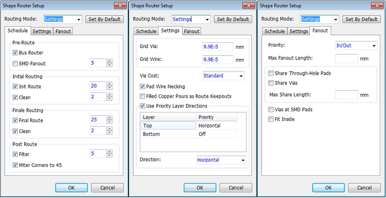
Select the Routing Mode: Settings or DO-file.
When in the Settings routing mode, you can define the following autorouter parameters using the tabs:
Schedule
Bus Router – create parallel traces between the pads connected via busses.
SMD Fanout – create fanouts for SMD pads before starting the autorouting, the value sets the number of passes.
Init Route – initial routing when the autorouter allows for design rule violations, the value sets the number of passes.
Clean – clean the design violations, created with Init Route feature, the value sets the number of passes.
Final Route – final routing, the value sets the number of passes.
Clean – clean any design rule violations that the Final Route feature may induce, the value sets the number of passes.
Filter – remove all design rule violations and excess vias, optimize the traces. New violations are not allowed in this step. The Filter's value sets the number of passes.
Miter Corners to 45 – miter corners to 45 degrees, otherwise traces will have 90-degree corners.
Settings
Grid Via – via placing grid.
Grid Wire – the trace placing grid.
Via Cost – set the cost of each via for the autorouter when drawing traces. The drop-down list has the following options: Standard – default via cost, Forbidden – route without vias, High – fewer vias, Low – more vias, Free – free to place any number of vias.
Pad Wire Necking – allow the autorouter to neck down the traces when connecting wide traces to narrow pads.
Filled Copper Pours as Route Keepouts – filled copper pours are counted as route keepouts.
Use Priority Layer Directions – define priority directions for the traces on different PCB layers. Forbid autorouter to draw traces on certain layers (single-sided circuit boards).
Direction – the direction of traces on selected layer.
Fanout
Priority – priority directions of the fanouts.
Max Fanout Length – maximum trace length from pad to fanout via.
Share Through-Hole Pads – use nearby through-hole pads of the same net instead of creating new fanout vias.
Share Vias – use nearby vias of the same net instead of creating new fanout vias.
Max Share Length – maximum trace length when sharing nearby through-hole pads or vias.
Vias at SMD Pads – place vias inside SMD pads.
Fit Inside – center vias inside SMD pads.
3.8.16. Electra/Specctra integration
DipTrace allows the user to route DipTrace circuit boards with external Electra and Specctra autorouters.
You need to export layout into *.dsn format, then route the circuit board in Electra or Specctra autorouter, and import completed layout back into DipTrace.
To export a *.dsn file, select "Route \ Electra/Specctra Interface \ Export Autorouter DSN" or "File \ Export \ Autorouter DSN" from the main menu.
To import the routed project from *.ses file, select "Route \ Electra/Specctra Integration \ Import Autorouter SES" or "File \ Import \ Autorouter SES" from the main menu.
Do not make any changes to the design on the stage before importing the *.ses file from external autorouter.
3.8.17. Hierarchy blocks
DipTrace PCB Layout is capable of arranging components by hierarchy blocks directly on the board and copy placement and routing between hierarchical blocks. Go to "Route \ Hierarchy" from the main menu. If the source schematic does not have hierarchy blocks, this dialog box will be blank.
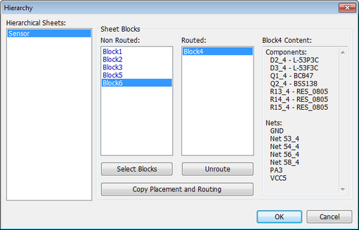
Sort components by hierarchical blocks
Select schematic sheet from the Hierarchical Sheets list, then select hierarchy block from the Non Routed Sheet Blocks list (you can select several blocks at a time with Ctrl key), then press the Select Blocks button to arrange components by selected blocks on the design area.
Copy placement and routing between blocks
Route traces inside the hierarchical block and change the layout of components, then open the Hierarchy dialog box, select routed and non-routed blocks, and press Copy Placement and Routing button to copy placement and routing between the hierarchical blocks.
Traces connecting the components inside the hierarchical block to components outside the block are not copied.
3.9. PCB Calculators
The PCB Calculator is a versatile and comprehensive tool designed to enhance the PCB design process. It enables precise calculations and design optimizations across several critical aspects of PCB design. With this tool, users can:
Calculate Trace Width: Determine the appropriate width for PCB traces to handle specific currents without exceeding permissible temperature rises. This ensures the reliability and performance of the electrical connections on the board.
Determine Electrical Spacing: Calculate the necessary spacing between traces for circuits operating at specific voltages to prevent short circuits and ensure compliance with safety standards.
Analyze Transmission Line Parameters: Evaluate the properties of transmission lines, which is essential for high-frequency signal transmission. This includes calculating impedance, propagation delay, and signal integrity parameters to ensure that signals are transmitted with minimal distortion and loss.
Evaluate Differential Pairs: Optimize the design of differential pairs used in high-speed digital and communication circuits. This involves calculating the spacing and trace width needed to maintain consistent impedance and minimize noise, ensuring accurate and reliable data transmission.
Design and Place Planar Inductors: Create, place, and save planar inductors directly within the PCB design. Planar inductors are used in various applications such as power supplies and RF circuits, and this feature allows for their seamless integration into the PCB layout.
By leveraging the capabilities of the PCB Calculator, designers can ensure that their PCB designs meet electrical performance requirements, safety standards, and reliability criteria, ultimately leading to more robust and efficient electronic products.
3.9.1. Trace Width Calculator
To use this tool, select a trace and go to Tools/ PCB Calculator. In the Trace Width tab the Selected Trace’s details (its name, width, length and layer) will be displayed at the top.
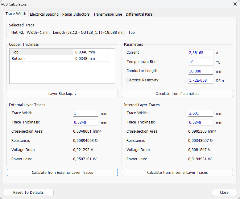
The Copper Thickness section shows the thickness of copper conductors in different layers. To modify this value, click the Layer Stackup button.
The Parameters section allows you to set values for calculating the trace width required to carry a given Current while keeping the increase in the conductor temperature below a specified limit (Temperature Rise). Conductor Length and Electrical Resistivity fields are filled automatically for the selected trace. Press Calculate from Parameters to obtain Trace Width for conductors in both the External and Internal Layers, displayed below. The Cross-section Area, Resistance, Voltage Drop, and Power Loss are also calculated.
Click Calculate from External Layer Traces to compute the parameters using the provided External Layer Trace Width and/or Thickness values.
Similarly, click Calculate from Internal Layer Traces to calculate the parameters based on the Internal Layer Trace Width and/or Thickness input values.
Press Reset to Defaults to set default values.
3.9.2. Electrical Spacing Calculator
To use this tool, select a trace and go to Tools/ PCB Calculator.
In the Electrical Spacing tab, select the conductor type and use the table to find the electrical spacing value for specific voltages as established by IPC-22221B PCB Clearance standards.
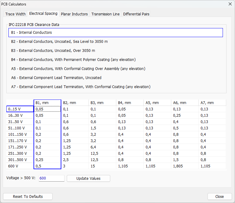
If your circuit is designed to operate at voltages higher than 500 V, enter the value in the Voltage > 500V field and press the Update Values button. The clearance calculated for the entered voltage will be displayed in the last line.
3.9.3. Planar Inductors
A planar inductor is a pattern that consists of copper windings. Designing planar inductors involves careful consideration of the trace width, spacing, and layer stacking to achieve the desired inductance and performance.
To create and place a Planar Inductor, go to Tools/ PCB Calculator and open the Planar Inductors tab. Alternatively, select Objects/ Place Planar Inductor from the main menu.
Choose Inductor Geometry, set Input Parameters: enter the Outer Diameter, Conductor Width and Spacing and the number of Turns. Press the Solve button for DipTrace to calculate the resulting Fill Factor, Inner Diameter and Inductance values.
Press Place to Layout to place the Planar Inductor directly to your design.
To save the Planar Inductor pattern for future use, press Save as New Library or Add to Existing Library.
Press Reset to Defaults to revert to default values.
3.9.4. Transmission Line/ Differential Pairs
In the PCB Calculator, the Transmission Line and Differential Pairs tabs provide tools for analyzing the electrical parameters of a transmission line based on its physical characteristics. Both dialogs are similar in functionality, with the key difference being that the Differential Pairs tab calculates a few additional parameters specific to differential pairs. For simplicity, we'll use the Transmission Line calculator as our example to explain how these features work.
To use this tool, select a trace and go to Tools/ PCB Calculator, open Transmission Line tab. The details of the selected transmission line (name, width, length and layer) will be displayed at the top of the dialog.
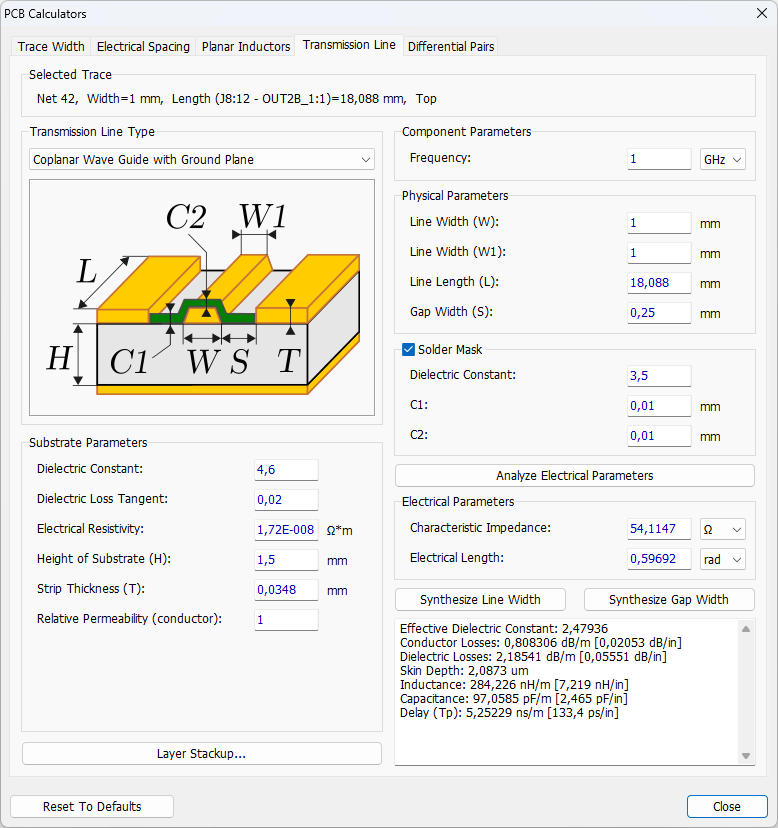
Transmission Line Type is determined automatically, based on the Layer Stackup, however, you can manually select a different type from the drop-down menu, if needed.
Substrate Parameters - Dielectric Constant, Dielectric Loss Tangent, Electrical Resistivity, Height of Substrate, Strip Thickness and Relative Permeability - can be modified manually to simulate various scenarios for analyzing purposes. Click Layer Stackup to change the Substrate type or properties.
Adjust Component Parameters along with Physical Parameters of the transmission line and Solder Mask characteristics as necessary. Once set, click Analyze Electrical Parameters. The resulting values of Characteristic Impedance, Electrical Length, Effective Dielectric Constant, Conductor Losses, Dielectric Losses, Inductance, Capacitance, and Delay will be calculated and displayed below.
For generating Line Width and Gap Width based on Characteristic Impedance and Electrical Length, input the desired electrical parameters and click Synthesize Line Width or Synthesize Gap Width.
To revert all changes, press Reset to Defaults to restore the original settings.
3.10. Verification
3.10.1. Check design rules
DRC works in regular (offline) and real-time modes. Real-time DRC checks all user actions on-the-go, according to the set of design rules, while the DRC in regular mode is launched by the user.
Select "Verification \ Check Design Rules" from the main menu or press  button on the Route toolbar to launch the DRC. Errors are marked with red circles (clearance errors) or magenta circles (size errors) directly on the design area. The list of errors allows the designer to navigate through the layout. It also contains the description of each error with the current value, target constraints, and information about where to change them.
To hide the errors, go to "Verification \ Hide Errors" from the main menu.
Notice that some design constraints (including the differential pair length/phase rules and length-matching rules) are set in the Net Classes and Length Matching dialog boxes.
Select "Verification \ Design Rules" from the main menu or press  button on the Route toolbar to open the Design Rules dialog box.
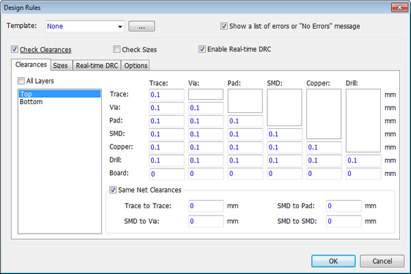
Here you can select a rule template. Press button to add/edit templates.
Show a list of errors or "No Errors" message checkbox allows for displaying the errors list or just the marks on the design area. Notice that DRC automatically checks the design right after autorouting.
Check Sizes checkbox is disabled by default. Therefore, you should enable it to verify the object sizes.
Enable or disable the Real-time DRC with the corresponding check box.
Tabs:
Clearance
It is possible to set up common clearance rules for all layers or for each PCB layer individually (uncheck All Layers checkbox, select layer, and specify required parameters). To set up detailed clearance, use the object-to-object grid table.
Check Same Net Clearances checkbox, and enter respective values, if you need to verify clearances between the objects of the same net.
Sizes
Set the minimum trace width, minimum and maximum drill sizes for plated and non-plated holes, and minimum/maximum ring sizes. Notice that each layer can have different parameters (uncheck All Layers checkbox, select layer, and specify the parameters).
Real-time DRC
If Real-time DRC is active, the user can specify the actions that are checked in the real-time mode: Routing and Creating/Editing Objects. Notice that checked item in the Real-time DRC tab means that you see the error circles before completing the corresponding action, and unchecked item is to report errors right after completing the action (assuming the Enable Real-time DRC checkbox is checked).
Options
1. Check Class-To-Class Rules – check class-to-class rules between the net classes.
2. Check Length Matching – consider length-matching rules (if any exist).
3. Check Copper Pours – verify copper pour clearances (may reduce the speed).
4. Check Route Keepouts – check if any route keepout shapes cross the copper areas or traces.
5. Check Courtyard – check for any overlays in the courtyard area.
6. Check Jumper Wires – check if any jumper wires overlay the copper objects.
7. Check Same Pattern Pads – check clearances between the pads of the same pattern.
8. Check Same Net Pads – check clearances between the pads of the same net.
9. Check Silk over Pads – check if silk shapes or text objects touch or overlay any pads; clearance value can be set here.
3.10.2. Check net connectivity
Net connectivity verification checks if all nets on the circuit board are properly connected (with traces, shapes or copper pours). We strongly recommend using this feature for boards with Power or Ground copper pours on signal or plane layers. The verification reports all isolated pads or copper pour areas.
Select "Verification \ Check Net Connectivity" from the main menu, then check the objects which you want to consider as connectors, and click OK.
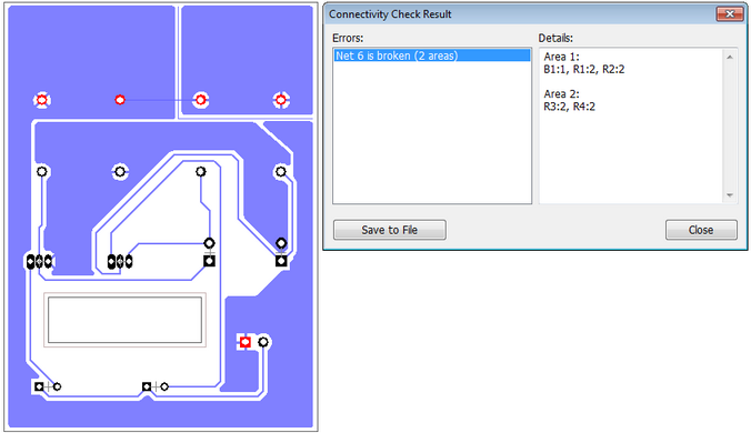
On the picture above you can see a simple example of a typical error, which breaks the copper pour net into several unconnected areas (Net 6 has 2 areas). If you have troubles finding the problem on the design area, check which pads of which components are disconnected, and use the Design Manager to find them on the design area.
We recommend using the net connectivity verification for all your projects.
3.10.3. Compare to schematic
To ensure that the net structure is correct, you can compare a completed circuit board to original schematic.
Select "Verification \ Compare to Schematic" from the main menu, and open your schematic file (*.dch extension). If there are any errors, DipTrace reports them in the list. Otherwise, the "No Errors" message appears.
Notice that new patterns and nets added directly in the PCB Layout (VCC, GND, etc.) cause no errors.
3.11. Working with layers
3.11.1. Review
All signal and non-signal PCB layers are available in the Layers tab on the right side of the screen (Design Manager panel).
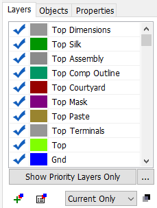
By default all layers are sorted from the top side of the board to the bottom. However, you can arrange them in the order you prefer and choose priority layers to be displayed in the list, with all other layers hidden. Press button to open Layer Priority and Order dialog.
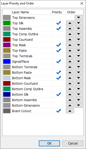
Tick the layers you want to be displayed in priority list; use  and
and  buttons to change their order in the list.
Press Show Priority Layers Only button to display only pre-established priority layers.
Press Show All Layers button to display all layers.
To select a layer, double-click it in the list. Copper layers have quick-access hotkeys in the brackets.
To show/hide layer on the design area, click on the corresponding blue check mark in the list. To change layer color, left-click on the color rectangle. Notice that the color of the traces, copper pours and SMD pads depend on the layer color.
To add a new signal/plane/non-signal layer, press  button, in the pop-up dialog box, define the layer properties, and press OK. To insert layer, right-click in the table row where you would like to insert a new layer, and select Insert Layer from the submenu.
Press  to open the Layer Setup dialog box which allows the user to add, delete, and edit signal, plane, and custom non-signal layers as well as manage physical properties of conducting and insulating layers of the layer stack.
Use the  drop-down to change the layer display mode. Press
  to adjust levels for the Contrast layer display mode.
3.11.2. Layer properties
Select "Route \ Layers Setup" from the main menu or press button on the Layers tab to change layer properties and manage the layer stack. The following dialog box pops up:
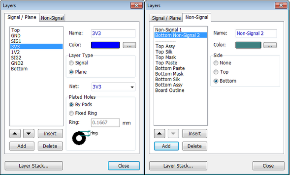
PCB layers can be divided into two physical types: Signal-conducting (copper layers) and Non-Signal layers (silk, paste, mask, etc.).
Signal layers are then divided into two logic types: Signal layers (for drawing traces) and Plane layers (for copper pours).
Tabs:
Signal/Plane
Move signal layers up and down, add, insert, and delete them, change layer name, color, and type (Signal or Plane). You can connect Plane layers to nets (usually PWR and GND) and specify plated hole parameters right below. To learn how to place copper pours and define thermals for plane layers, see the Copper Pour topic.
Non-Signal
Move custom non-signal layers up and down, add, insert and delete them, select the layer side (None means that layer is not connected to any side of the board), change layer color and its name.
Notice that default non-signal layers are separated from the custom non-signal layers. The user can not edit or delete default non-signal layers.
Layer stack
Press the Layer Stack button to get a full control over the stack of conducting and insulating PCB layers, their thickness, material, dielectric constant and total thickness of the circuit board. Document the stack of layers with a Layer Stackup Table.
3.11.3. Display modes
To change a layer display mode, select "View \ Layer Display" from the main menu or use the drop-down list on the Layers tab on the Design Manager.
DipTrace has the following modes to display the circuit board layers:
1. Current Only – only active layer is visible. Double-click on the layer in the Layers tab to select an active layer.
2. All Layers – all signal layers are visible. We recommend setting different colors for the layers.
3. Contrast – only active layer is at full contrast, other PCB layers are visible with reduced contrast. Go to "View \ Layer Display \ Contrast Level" or press button on the Layers tab to adjust the contrast level.
4. Contrast Edit – a special mode, which is the same as Contrast layer display mode, but you can edit objects on all layers without switching to them.This mode is available only from the main menu.
Notice that "Top Silk" and "Top Assembly" layers are active when the top or inner signal layer is selected, "Bottom Silk" and "Bottom Assembly" layers are active when the bottom signal layer is selected.
3.11.4. Layer stackup
DipTrace allows for comprehensive control over the stack of conducting and insulating PCB layers in the Layer Stack dialog box. Select "Route \ Layer Setup" from the main menu or press button on the Layers tab, then press Layer Stack in the Layer Setup dialog box.
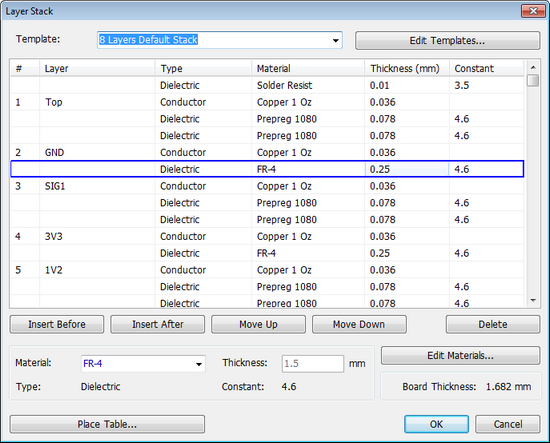
Here you can add/delete layers and move them up and down the stack. DipTrace automatically applies the most appropriate stack template depending on the number of signal/plane layers of the circuit board. You can select another template in the Template drop-down list or edit templates with the respective button.
Press Insert Before or Insert After to add a new layer and select its material, thickness (if allowed) and dielectric constant. To edit a layer, select it in the list, and change properties in the fields right below. To delete a layer, select it, and press Delete.
To document the layer stack, press Place Table.
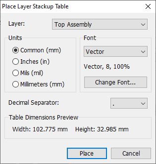
In the pop-up dialog box, select a non-signal layer for placing the layer stack table (Assembly, Silk or custom non-signal layers), change units and font, select decimal separator and check dimensions. Press Place, then left-click on the design area to place a layer stack table. The table is updated automatically, so can keep editing your layout after placing the table – all subsequent changes will be included into the report. Note that you can edit the table manually, however, auto-update mode will be disabled: left-click on any cell, a warning message will appear, click Yes – a Cell Properties dialog will appear, allowing you to change cell parameters and its content.
Layer thickness, which influences the via height, is taken into account by phase tune and trace length measuring tools.
Edit materials
DipTrace has a standard set of layer materials good for most users (copper conductors of various weight, FR-4, polyimide, prepregs, etc.) All materials are divided into three basic types: Conductor, Plane, and Dielectric. To edit standard materials or add new ones, press Edit Materials, and enter properties in the corresponding fields. Check Variable Thickness box to allow for changing the layer thickness directly in the Layer Stack dialog box.
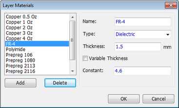
Use the corresponding buttons to add or delete materials to the list of available.
3.12. Printing, Sheet Setup
3.12.1. Printing
We recommend to use the Preview dialog box to print a layout, but you can also use the "File \ Print" main menu item or press the  button on the Standard toolbar to print the design directly from the main window.
Printing is similar to what you see on the design area. You can display the page borders and titles on the design area.
To change title properties, use the Titles and Sheet Setup dialog box. Use available title templates or create a new title block using the Title Block Editor.
3.12.2. Preview
To open the print Preview dialog box, select "File \ Preview" from the main menu or press  button on the Standard toolbar.
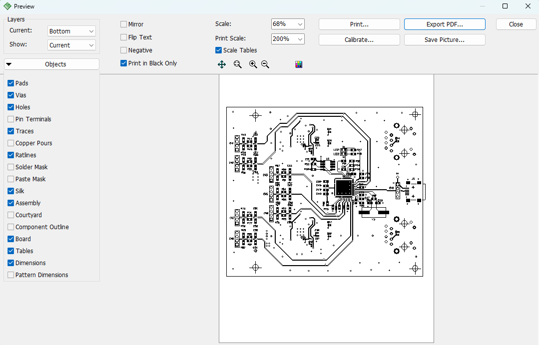
Move sheet in the preview area with the mouse.
You can see only active signal layer by default. To change the layer display mode or show another layer, use the Current and Show drop-downs in the Layers section of the Preview dialog box.
To show/hide the objects for printing, press the Objects button and check/uncheck necessary items in the pop-up drop-down menu.
The sheet is automatically scaled to fit the preview panel. To change the preview scale from 10% to 600%, use the Scale drop-down box. Use the Print Scale drop-down list to change the scale of the board relatively to the sheet. Use the Move Board tool ( button) to move the circuit board on the sheet.
If Scale Tables box is checked, DipTrace scales all tables when you scale the board.
To print mirrored design, check the Mirror checkbox. Flip Text check box mirrors all text objects. It is active only if "View \ Flip Text Automatically" main menu item is unchecked.
Press  button to set up the printing colors.
If you want to save the preview as a Bitmap or Jpeg image file, press the Save Picture button.
To save the layout as a PDF, click Export to PDF.
Press Calibrate to define horizontal and vertical correction factors to eliminate printing distortions induced by some printers.
3.12.3. Titles and sheet setup
To set up the sheet size, border margins, zones, titles, etc., select "File \ Titles and Sheet Setup" from the main menu or press button on the Standard toolbar.
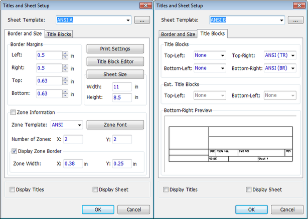
There are two tabs in the pop-up dialog box:
Border and Size
Define the sheet size, border margins, print settings, and zones. Zones are marked with numbers on top and bottom and with characters on the left and right sides of the border. ANSI and ISO zone marking standards are available. If Display Zone Border item is checked, the outer zone border appears on the design area. In this case, you can set the width of X and Y zone areas. Check Display Titles and Display Sheet checkboxes.
Title Blocks
Place up to four title blocks inside the sheet border (at all corners of the sheet) and two title blocks outside the border (in top-left and bottom-left corners). The last title block selected is shown in the title block preview field.
You can save the titles and sheet size as a sheet template, which can be used later to set all parameters at a time by selecting the corresponding template.
Use the Title Block Editor to create or edit title blocks, press Title Block Editor button in the Border and Size tab.
Sheet size and orientation depend on the printer settings. To manually change the parameters, press the Sheet Size button.
3.12.4. Title Block Editor
To open the Title Block Editor, select "File \ Title and Sheet Setup" from the main menu or press button on the Standard toolbar, then press the Title Block Editor button in the pop-up dialog box.
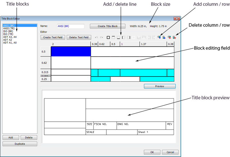
To create a new title block, press Add or press Duplicate to get a copy of selected title block, then select the block from the list of all title blocks, and press Create Title Block button. In the pop-up dialog box enter the width and height of the title block, set the number of columns/rows, and press OK. DipTrace creates a new block with columns and rows of equal size, depending on the total width/height of the block. Width and height of each column/row can be changed in the block editing area, just drag and drop the size field borders (cells on the top and left) or click them and enter exact size values.
To create a text field, select one or several cells in the Block editing area, and press Create Text Field button. In the pop-up dialog box enter the text, select font, font parameters, alignment, and press OK or leave it blank to add text later on the sheet.
Field borders highlight in red, they are invisible on the sheet. To draw or erase field border lines on the invisible cell borders, select required cell/s, and press Add/Delete Line buttons.
Notice that cells without a field are shown with gray color, regular fields (blank text fields) – with white color, fields with predefined text – with aqua color, selected cells – with dark blue color.
3.13. 3D preview & export
3.13.1. 3D PCB preview
Download and install the standard library of 3D models, which we offer for free on our website.
DipTrace PCB Layout has integrated 3D real-time preview module with MCAD export. 3D preview allows the user to see a printed circuit board in three dimensions with all electronic components installed, rotate board model in any direction and zoom in/out in real time.
Select "Tools \ 3D Preview \ 3D Visualization" from the main menu or press  button on the Standard toolbar. Typically, a 3D model is connected to the component pattern in the Pattern Editor, if a current project has components without 3D models attached, the following dialog box pops up.
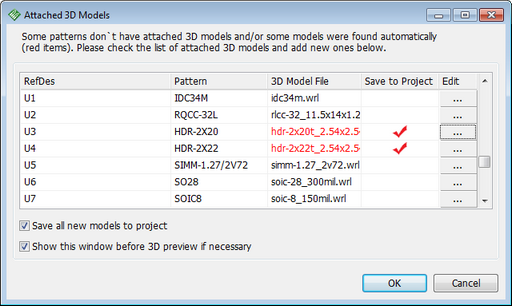
DipTrace searches for 3D models automatically when you launch the 3D preview in the PCB Layout. Red items in the list of components mean that 3D models were either found automatically or attached manually, black items – components with pre-attached 3D models, if the 3D Model File field is blank – component does not have a 3D model, and DipTrace could not find a suitable one. Press  button in the corresponding row of the list to connect or remap a 3D model to the component.
To save all found 3D models, check Save all new models to project checkbox or double-click in the Save to Project field in the table. Otherwise, all newly found models stay connected only for existing 3D preview session.
Go to the Pattern and Model Search Options dialog box to configure the search parameters.
If you do not want to see this dialog box when launching the 3D preview, uncheck Show this window before 3D preview if necessary checkbox.
Press OK to launch the 3D Preview.
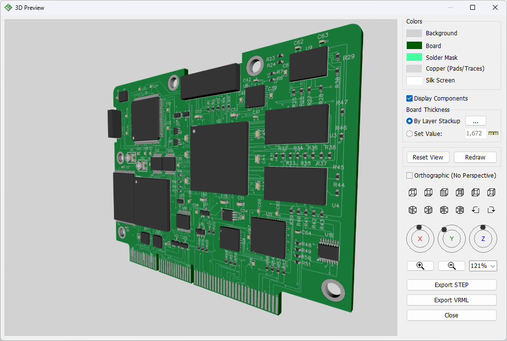
Use the left mouse button to rotate the circuit board model around X or Y axes, press the mouse wheel (middle button) to rotate around the Z axis, hold the right mouse button to pan, and scroll the mouse wheel to Zoom In/Out.
You can also use side and isometric view buttons for quick change of 3D display perspective.
Change the colors of the board, silkscreen, solder mask, and copper areas. Untick Display Components if you want to preview your PCB only.
Board thickness can be defined:
By Layer Stackup (press button to open Layer Stackup dialog and view or edit the values)
By a custom value
Press Redraw button to apply changes.
Press Reset View to return all coordinates to 0.
Orthographic (no perspective) - enable for the board preview to be rendered using an orthographic projection. This allows to avoid visual distortion by perspective and maintain consistent scale of objects across the view.
The solder mask layer is transparent, and sometimes it is hard to get a proper color of the board. We recommend defining similar colors for solder mask layers and the board.
3.13.2. 3D export
DipTrace 3D Preview module allows the user to export 3D model of the board to STEP (*.step) and VRML 2.0 (*.wrl) formats. These are supported by most mechanical CAD software.
When in the 3D Preview & Export module ("Tools \ 3D Preview \ 3D Visualization" from the main menu), press Export STEP button, in the pop-up dialog box specify the export objects and select the model export mode.
Notice that exporting holes dramatically slows the export process. We recommend exporting a project as a solid body in the STEP format.
STEP model does not include the copper traces.
Press Export VRML button, select which objects to export (Board, Package Models, Pad Holes, Copper Layers, Silk Layers), set the units and file location.
VRML model includes the copper traces (unlike STEP). VRML is good for demonstration purposes.
3.13.3. Attach a 3D model
Please make sure that you have installed the standard library of 3D models, which we offer for free on our website.
To attach a 3D model, right-click on the component on the design area, and select 3D Model from the submenu. The following dialog box pops up:
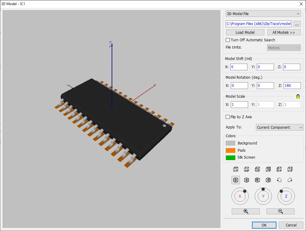
Use the left mouse button to rotate a 3D model around X- or Y-axes, press the mouse wheel (middle button) to rotate around the Z axis, hold the right mouse button to pan, and scroll the mouse wheel to zoom in/out. You can also change the color of the background, pads or silk layer.
You can also use side and isometric view buttons for quick change of 3D display perspective.
If a component does not have a 3D model attached, you will see only the component's footprint.
There three ways to add a 3D model to a component package. You can select the option that suits you from a drop-down in the upper part of the dialog.
| 1. | Load 3D Model file. Press All Models >> button to open the list of all available 3D models in the active library. Select model from the list, and preview it immediately (3D models in the list are organized by pattern libraries). |
Notice that models in the VRML and STEP formats are in different categories in the list (both have "models3d" name).
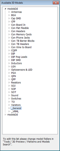
If the All Models list is empty, you need to install the standard library of 3D Models from our website or check the search folders in the Pattern and Model Search Options dialog box.
To attach a 3D model from the separate file, press the button to specify the path to the file on your computer. DipTrace supports 3DS, VRML, STEP, and IGES files.
| 2. | IPC-7351 Model Generator. This option is available only if Pattern Generator was used to make a footprint. |
| 3. | Create a 3D model by Component Outline. To use this option, a component has to have an outline. To place it, open the component in Pattern Editor, go to Objects/ Precise Shape Placement and place a shape within the component's silk screen boundaries in the Top Outline Layer. Specify the model height and DipTrace will generate a 3D shape to mimic a device. This option can also be used if there is no 3D model for a footprint designed in the Pattern Generator. It suits best for SMD parts. |
Mapping a 3D model
DipTrace automatically places a 3D model to fit the pattern's drawing, but sometimes you may need to adjust a 3D model location or its scale. Just enter appropriate values into the corresponding fields - Model shift, rotation angle, and scale by each axis. Changes are applied instantly.
3.13.4. 3D model search
DipTrace loads 3D models from the specified folders and attaches them to the components without 3D models by comparing the component pattern with available 3D models. To configure the search process and define the folders where the software should search for 3D models, go to "Tools \ 3D Preview \ Pattern and Model Search" from the main menu. The following dialog box pops up:
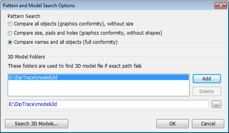
The Pattern Search section allows the user to choose how to compare patterns with 3D models. These settings apply to all components without attached models when you launch the 3D preview.
3D Model Folders – let the software know where to search for 3D models. You can add/delete folders to the list. By default, all 3D models are in the "models3d" folder inside the "DipTrace" directory.
Press the Search 3D Models button to launch the search and verify new settings.
Notice that standard 3D libraries are not included in the DipTrace installation package. You need to download them from the DipTrace website.
3.14. Plugins
DipTrace supports plugins, allowing the software's functionality to be extended and customized according to users' needs. This means that users can enhance their design process by adding specific features or automations that are not available in the default software.
Plugins can be created using any programming environment, offering flexibility to developers with different coding preferences and expertise. Whether you are proficient in C++, Python, or another programming language, you can develop plugins to integrate seamlessly with DipTrace.
To help users get started, DipTrace provides sample plugins along with their source codes. These examples serve as a valuable resource for learning how to develop and implement plugins. Two sample plugins include:
Converting Shapes to Dash/Dot Lines: This plugin allows users to convert selected shapes in their design into dashed or dot-dashed lines. It offers customization options for units, line types, and sizes of dashes and dots.
Removing Solder Mask for Selected Traces: This plugin enables users to remove the solder mask over selected traces and shapes located in signal layers. It provides options for selecting nets or their segments and adjusting mask swell.
3.14.1. Convert selected shapes to Dash/ Dot
To convert a shape to a dash line, place and/ or select it in your design. To run the plugin go to Tools/ Plugins in the main menu and select Convert selected shapes to Dash/ Dot.
If you don't have .NET 8.0 installed, you will be prompted to install it.
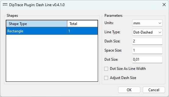
In the pop-up dialogue set the Parameters as required:
Units: mm, mil, inch
Line Type: Dashed or Dot-Dashed
Dash and Dot Size and the Space between the elements.
Mark Dot Size as Line Width to automatically adjust the dot size to match the Line width.
Mark Adjust Dash Size to allow the software to determine the dash size.
Click OK to apply the changes.
Click Cancel to discard changes.
3.14.2. Open Solder Mask for Selected Traces
To run the plugin that removes solder mask over traces and shapes in signal layers select one or multiple objects, then go to Tools/ Plugins/ Open Solder Mask for Selected Traces.
In the pop-up dialog set the Parameters as required.
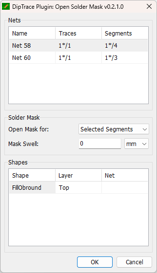
Next, choose from the drop-down menu whether to Open Mask for Selected Segments, Traces or entire Nets.
Set Mask Swell, if necessary.
In the Shapes section the selected shapes will be displayed.
Click OK to apply.
Click Cancel to discard changes.
4. Component Editor
4.1. User interface
4.1.1. Main window
Component Editor main screen includes the symbol design area, the main menu, toolbars, the Library Manager panel, the Component Properties panel, and the status bar.
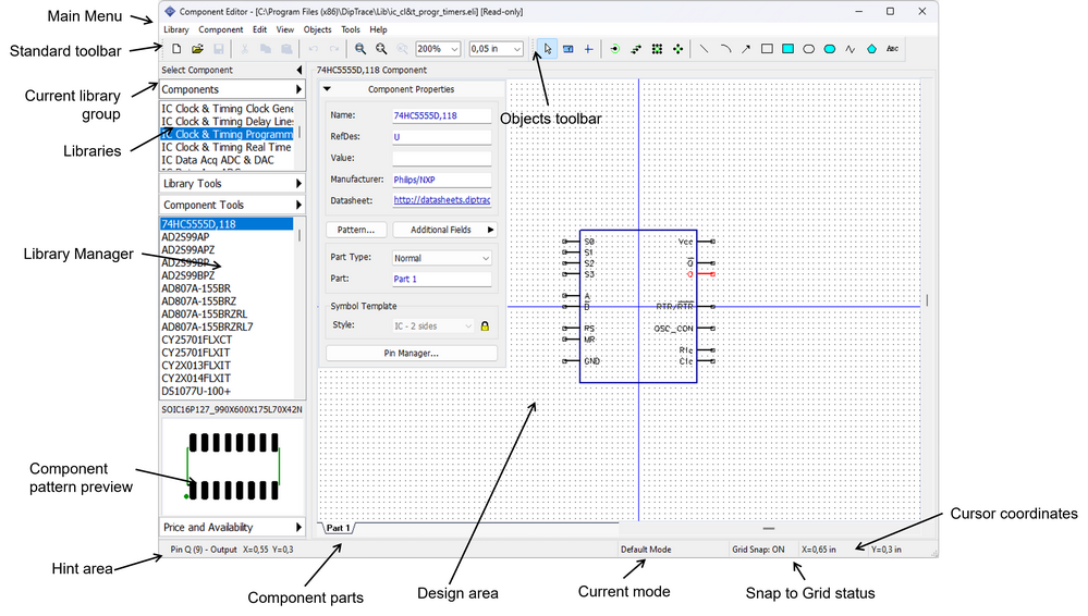
In the symbol design area you can create and edit the symbol (pins, shapes, text, etc.).
All common functions can be found in the main menu. There are the following items: Library, Component, Edit, View, Objects, Tools, Help.
Other interface elements:
Standard toolbar – file-management tools, cut/copy/paste objects, change scale and grid size.
Objects toolbar – switch to default mode, define origin, create and edit pins, shapes and text objects.
Library Manager – component management tools, component libraries sorted by library groups, user libraries. Select library from the list and component from the list below. Set up libraries, add/edit/delete library groups, manage search filters, verify libraries etc.
Component Properties panel – basic component-building tools. It is possible to create a component according to a template. This panel is located on the design area. It is possible to show/hide the component properties panel or minimize it.
4.1.2. Toolbars
Component Editor has two main toolbars, a Library Manager panel and a Component Properties panel.
Standard toolbar

Contains the following tools:
New – create new component library. If a previous library was not saved, DipTrace will offer to do that. Component Editor works only with one library at a time. Saving changes is required before switching to another library.
Open – open existing component library (*.eli) file. If library is not in the DipTrace system it will be automatically added to Other Libraries library group.
Save – save current component library. If a library has never been saved, a special dialog box will offer to save it. If a library already has corresponding *.eli file, it will be saved automatically into that file. This tool is active only for unsaved changes.
Cut – move selected object/s to the clipboard.
Copy – copy selected object/s to the clipboard.
Paste – paste object/s from the clipboard.
Undo – one editing step backwards.
Redo – one editing step forward. It is active only after using the Undo tool. If you've edited component after using the Undo tool, Redo tool becomes inactive.
Zoom Window – set current scale and pan component to defined window.
Zoom Extents – set current scale and pan layout to show all objects.
Undo Zoom – return to the previous scale and panning.
Scale – define design area scale (from 25% to 800% or type in a new value). Changing the scale is also possible with the mouse wheel, Plus sign (+) and Minus sign (-) default hotkeys or in the main menu.
Grid Size – select current grid size from the drop-down list or type in a new value.
Objects toolbar

Contains tools to switch to default mode, measure length, define origin, place pins (single, pin line, pin rectangle, pin circle), create shapes (line, arc, arrow, rectangle, filled rectangle, obround, filled obround, polyline, polygon) and text. Pin placement parameters control the number, size and shape of the pin.
Component Properties panel
|
This panel allows the user to change properties of the current component. It has all the necessary tools for creating a typical component and buttons for most basic and necessary features: Attach Pattern and Pin Manager.
There are 4 symbol styles: Free, 2 sides (two pin lines), IC - 2 sides (two pin lines and shape) and IC - 4 sides (4 pin lines and a shape).
It is possible to create component using another component as a template. This panel allows the user to enter/edit component name, RefDes, value, manufacturer, datasheet and additional fields. Name, RefDes, Manufacturer and Datasheet fields are assigned for the entire component, Value and Part Name may vary for different component parts (multi-part components). The similar parts are united by name.
There are 3 part types: Normal, Power and Gnd and Net Port. Component can contain only one part of Power and Gnd type. This part can be hidden in the Schematic by checking the "View \ Hide Power and Gnd" main menu item. Net Port part can be used to connect wires on different design areas/pages (GND, VCC, etc.)
Lock basic parameters to prevent accidental changes. |
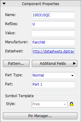
4.1.3. Status Bar
Status bar is located in the bottommost part of the Component Editor window.

It shows the following information:
Hint - standard hint containing information about the selected object on the design area.
Mode - shows the current mode (Default, Place Pins, Place Shape, etc.).
Grid Snap - the current Snap to Grid status.
X, Y - coordinates of the current position of the cursor or selected element.
4.1.4. Library Manager panel
|
Library Manager panel provides access to all necessary library and component management tools. This panel consists of two lists and several buttons.
Library list
Select library from the list and all components from selected library will be available in the component list right below.
Library Setup dialog box allows the user to add/delete libraries to/from the library groups and add/delete new library groups. Library management is cross-module – all groups and libraries customized in other DipTrace software modules (Schematic, PCB Layout and Pattern Editor) will be instantly available for editing here. Component Editor works only with components.
Components list
All components of selected library.
Hide component selection panel by pressing the small arrow near "Select Component" text. Left-click on the component to open it on the design area or right click it to open the submenu with all component tools. To change the size of the Library Manager panel, hover over its right border, left-click and drag it. |
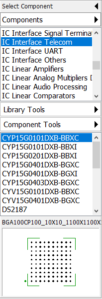
 – find components, insert new components into current library or another library, move components up and down the list, copy and move components between the libraries, duplicate, and delete them.
4.1.5. Main menu
4.1.5.1. Library
New – create new component library. If current library has unsaved changes, the DipTrace will offer to save it.
Open – open existing component library (*.eli or .elixml) file.
Open Recent – last five component libraries.
Save – save current component library. If library has never been saved, a special dialog box will offer to do that. If library already has a corresponding *.eli file, it will be saved automatically into that file. This tool is active only when there are unsaved changes.
Save as – open the save dialog box to save component library into selected file.
Import – import component libraries and pin names from various formats.
Export – export library to DipTrace ASCII format.
Library Setup – add/delete/copy/move libraries to/from the library groups, add/delete new library groups. Library management is cross-module, hence all groups and libraries customized in other DipTrace modules (Schematic, PCB Layout and Pattern Editor) will be available for editing here.
Name and hint of <current library> – define name and hint for active library.
Sort Components in <current library> – sort components of current library by name.
Check <current library> – general library information (total number of components and pins) verification for possible errors and error report in the same dialog box.
Open Templates – open component template library.
Save Templates – save current library as component template library file.
Exit – close the Component Editor. If current library is not saved, DipTrace will offer to do that.
4.1.5.2. Component
Find Component – search component by name, RefDes, value, pattern, datasheet, manufacturer, additional fields etc.
Search Parts at SnapEDA – search SnapEDA libraries directly from within DipTrace.
Add New to <current library> – add new component to current library.
Insert New to <current library> – insert new (blank) component to the library (into current position).
Insert from Another Library – insert component from another library into current position.
Duplicate Selected – duplicate selected components.
Move Up – move current component up in the list.
Move Down – move current component down in the list.
Move to the end – move current component to the end of the list.
Copy to Another Library – copy selected component to another library.
Move to Another Library – move selected component to selected library.
Clear <current component> – delete all content of selected component.
Delete from Library – delete current component from the library.
Add New Part – add new part to current component (multi-part components).
Create Similar Parts – create a group of similar parts based on current part (for multi-part components).
Insert New Part – insert new part into current position (for multi-part components).
Delete Current Part – delete current part (for multi-part components).
Change Symbol Style – convert symbol style to "IC - 2 sides" or "IC - 4sides" automatically.
IC Pin Repositioning – sort pin positions by names or by numbers, it is possible to set the order and direction of pin placement.
Make Buses from Pins – extract buses from pin names, pins are placed to the left from the symbol.
Pin Manager – open the Pin Manager for current component.
Attached Pattern – open the dialog box to attach pattern to component. Pattern is selected from a pattern library (*.lib). It is possible to change pin numbers (attached pattern pads) in the Pin Manager dialog box.
SPICE Model – define/change spice parameters for current component (device type, model, pin-to-signal map etc.).
Pad Signal Delay – define any additional distance that a signal propagates within a component. This value is considered for phase and length tuning.
Pin Numbers – set pin display options for current component. There are 3 states: Show – show pin numbers, Hide – hide pin numbers, Default – use general software settings. These are not general pin display settings found in the "View \ Pin Numbers" main menu item.
Default Additional Fields – define default additional fields for all newly created components or change additional fields for all components of active library at a time.
4.1.5.3. Edit
Undo – one editing step backwards.
Redo – one editing step forward. It is activated only if Undo has been used. If you edit component after using Undo, the Redo tool becomes inactive.
Cut – move selected objects to the clipboard.
Copy – copy selected objects to the clipboard.
Paste – paste objects from the clipboard.
Delete – delete selected objects.
Select All – select all objects of current symbol.
Edit Selection – select objects by type etc.
Rotate – rotate selected objects 90 degrees counter-clockwise.
Rotate Group – rotate selected objects as a group.
Flip Group – flip selected objects as a group horizontally or vertically.
Align Objects – align selected objects horizontally or vertically and distribute them equally.
Group – group selected objects.
Ungroup – ungroup objects.
Lock Selected – lock moving and editing of all selected objects.
Unlock Selected – unlock moving and editing of all selected objects, if they were previously locked.
Rotate – rotate selected objects 90 degrees counter-clockwise.
Rotate Group – rotate selected objects as a group.
Flip Group – flip selected objects as a group horizontally or vertically.
Align Objects – align selected objects horizontally or vertically and distribute them equally.
Center Symbol – center current symbol with respect to zero point.
Rotate Symbol – rotate current symbol 90 degrees clockwise with respect to zero point.
Flip Symbol – flip the current symbol horizontally or vertically with respect to the zero point.
4.1.5.4. View
Toolbars – show/hide the component properties panel, Standard toolbar and the Objects toolbar.
Display Hint – display hint for objects on the design area. Hint is also duplicated in the bottom-left corner of the screen.
Pin Numbers – change default pin number display options.
Move Text Tool – move pin names and pin numbers.
Pin Colors by EType – set colors for pins of different electric type. May be very helpful for pin placement.
Scale – change the scale in the submenu. Press Plus sign (+) or Minus sign (-) to zoom in/out.
Units – change the measurement units (mm, mil or inches).
Precision – adjust precision rate for the project values and the grid.
Display Origin – show/hide the part origin.
Define Origin – define component origin by the mouse pointer or by coordinates (incremental to existing origin).
Axis Color – change axis color for the origin.
Grid – show/hide the grid.
Grid Size – change grid size (standard sizes or custom).
Customize Grid – edit/create new grid sizes.
4.1.5.5. Objects
Place Pins – place pins, various pin formations.
Place Shape – place various shapes.
Place Text – place text.
Pin Placement Setup – change default pin placement settings (pin type and pin-to-pin spacing).
Measure – the ruler tool for measuring any sizes/distances directly on the design area.
Precise Shape Placement – place shape by defining by defining its parameters and coordinates.
Precise Pin Placement – place pins by defining pin parameters and coordinates or key points of a pin shape.
4.1.5.6. Tools
Bulk Update of Patterns – allows for bulk substitution of patterns in all the component libraries of the selected directory with new ones contained in pattern libraries of a specified folder; the substitution is done by pattern name.
HotKey Settings – define keyboard shortcuts for dialog boxes and tools.
Environment Variables – define and manage environment variables.
Pattern Editor – launch the Pattern Editor.
Schematics – launch the Schematic.
PCB Layout – launch the PCB Layout.
4.1.5.7. Help
Component Editor Help – open Component Editor help file.
DipTrace Tutorial – open DipTrace tutorial in PDF format.
Request Support – DipTrace technical support portal.
Library Design Service – online request form for library design service (performed by experienced engineer).
DipTrace Home Page – DipTrace official website.
About – information about current version and edition of DipTrace.
4.1.6. Object submenus
4.1.6.1. Pin
To open the pin submenu, right click on any pin.
Pin Name – change pin name. To show/hide inversion, use the Tilde (~) key.
Pin Array Names – name all selected pins automatically by template, for example, bus with A0 to A31 pins.
Lock Selected – lock moving and editing of all selected objects.
Unlock Selected – unlock moving and editing of all selected objects, if they were previously locked.
Rotate – rotate selected objects 90 degrees counter-clockwise.
Rotate Group – rotate the group of pins.
Flip Group – flip the group of pins.
Align Objects – align selected objects horizontally or vertically and distribute them equally.
Snap to Grid – snap the selected pins to grid, when the grid is on, but Snap to Grid option is disabled for the overall project.
Rotate – rotate selected objects 90 degrees counter-clockwise.
Rotate Group – rotate the group of pins.
Flip Group – flip the group of pins.
Align Objects – align selected objects horizontally or vertically and distribute them equally.
Cut – move selected object/s to the clipboard.
Copy – copy selected object/s to the clipboard.
Delete – delete selected object/s.
Group – group selected objects.
Ungroup – ungroup objects.
Pin Manager – the Pin Manager dialog box.
Pin Properties – change pin properties.
4.1.6.2. Shape
Right click on any shape to open this submenu:
Lock Selected – lock moving and editing of all selected objects.
Unlock Selected – unlock moving and editing of all selected objects, if they were previously locked.
Insert Point – insert point to the polyline or polygon.
Delete Point – delete point from polyline or polygon.
Rotate – rotate selected object/s 90 degrees counter-clockwise.
Align Objects – align selected objects horizontally or vertically and distribute them equally.
Snap to Grid – snap selected shapes to the grid, when the grid is on, but Snap to Grid option is disabled for the overall project.
Cut – move selected object/s to the clipboard.
Copy – copy selected object/s to the clipboard.
Delete – delete selected object/s.
Group – group selected objects.
Ungroup – ungroup objects.
Points – change key points for selected shape.
Properties – change parameters of the selected shape.
4.1.6.3. Text
Right click on any text to open this submenu:
Current Text – launch Edit Text dialog box. Here you can change the text, its alignment, line spacing or open Text Properties for more detailed text settings.
Show – automatically show the Text, Name, RefDes, Value, Part Name (current part) of the component, Manufacturer or Datasheet; there’s no need to manually type these values.
Font Type – change font type for text object (Vector, TrueType). Unicode characters are supported only in the True Type mode.
Font – change the font of the text. Text object is scaled automatically.
Lock Selected – lock moving and editing of all selected objects.
Unlock Selected – unlock moving and editing of all selected objects, if they were previously locked.
Rotate – rotate selected object/s 90 degrees clockwise.
Align Objects – align selected objects horizontally or vertically and distribute them equally.
Snap to Grid – snap selected text object to grid, when the grid is on, but Snap to Grid option is disabled for the overall project.
Cut – move selected object/s to the clipboard.
Copy – copy selected object/s to the clipboard.
Delete – delete selected object/s.
Group – group selected objects.
Ungroup – ungroup objects.
Properties – adjust the properties of a text object, such as line spacing, alignment, angle of rotation, location and coordinates of anchor point, font type and font settings (size, line width, text width).
4.1.7. Modes of operation
There are several modes of operation:
Default is the mode set by default. It becomes active as soon as you start the program. To return to this mode while in any other mode, you need to right click on empty area or choose  tool on the Objects toolbar. This mode allows the user to:
– select and move objects.
– change sizes of shapes and texts.
Measure mode. Select measuring tool from the main menu ("Objects/ Measure") or press  on the Objects toolbar. Left-click in the starting point and move the mouse pointer to the end point keeping left button pressed. The length will be displayed in the bottom-left corner, in the hint area.
Define Origin mode. Select Define Origin tool from the main menu (View/ Define Origin/ By Mouse Pointer) or press  on the Objects toolbar. Left-click in the design area to establish a new Origin point.
Place Pins – select pin placement tool from the main menu ("Objects \ Place Pins") or press  button on the Objects toolbar to enable this mode. It is possible to place a single pin, pin line, rectangle or a circle of pins. Pin-to-pin spacing and pin type are defined in the Pin placement setup dialog box ("Objects \ Pin Placement Setup"). If you are not satisfied with visual placement, there is a precise pin placement tool ("Objects \ Precise Pin Placement").
Place Shapes – select shape placement tool from the main menu ("Objects/ Place Shape") or press the corresponding button on the Objects toolbar to enable this mode. Specify the key points one-by-one in order to place the shape. If you are not satisfied with visual shape placement, there is a precise placement tool ("Objects/ Precise Shape Placement").
Place Text mode. Select text placement tool from the main menu ("Objects/ Place Text") or press  button. Left-click on the design area and type a text. DipTrace supports multi-line text placement. Select Current Text item from the right-click submenu to change the text, line spacing and alignment. Use Text Properties dialogue, launched by selecting Properties item from the right-click submenu, to adjust other text properties: font, layer, text angle, anchor point location, etc.
Move Pin Names and Numbers – this mode allows the designer to move pin names and numbers with respect to the pins. Select "View/ Move Text Tool" from the main menu or press F10 key to activate this mode.
4.1.8. Hotkeys
DipTrace features customizable hotkeys in all software modules. To open the HotKey Settings dialog box, proceed to "Tools \ HotKey Settings" from the main menu in any of the DipTrace modules: Schematic, PCB Layout, Component and Pattern Editors. The designer can view or assign custom keyboard shortcuts for various tools, actions and dialog boxes by left-clicking in the corresponding field and pressing a keyboard combination.
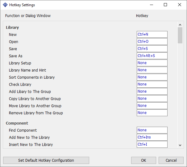
If the combination is already in use, a warning message comes out. Notice that certain shortcuts are reserved by the program and are not customizable. Press OK to apply changes. To restore default configuration press the Set Default Hotkey Configuration button.
Hotkeys reserved by the system:
Ctrl Shift Shift + mouse Enter Esc Left arrow Right arrow Up arrow Down arrow Shift + S Alt+any key |
– hold down to invert selection; – hold down to add objects to selection; – orthogonal moving of selected objects; – complete action; – cancel action; – move object left, pan left while routing/building; – move object right, pan right while routing/building; – move object up, pan up while routing/building; – move object down, pan down while routing/building; – enable disable auto-panning; – reserved by the system. |
4.1.9. Environment Variables
According to DipTrace License Policy, the software can be used by one license holder on several devices. To ensure smooth portability of your projects, DipTrace features an Environment Variables tool that allows setting variables for the paths to directories containing libraries, 3D models, images, etc. on different machines.
Go to Tools/ Environment Variables to open the Environment Variables dialog.
In the Common Variables section you can see the paths used by the software during installation and the corresponding variables for those paths.
In the User Variables part you can establish new variables for the paths to the directories, where your libraries or 3D models are stored. Type the variable in the Variable cell and set the path in the Folder line or press  button and select Browse for Folder to select the directory. Use the same variable on another PC to associate it with the path to the required folder on that machine. In this way when switching between machines the software will look for the files using the path corresponding to the established variable on the given PC.
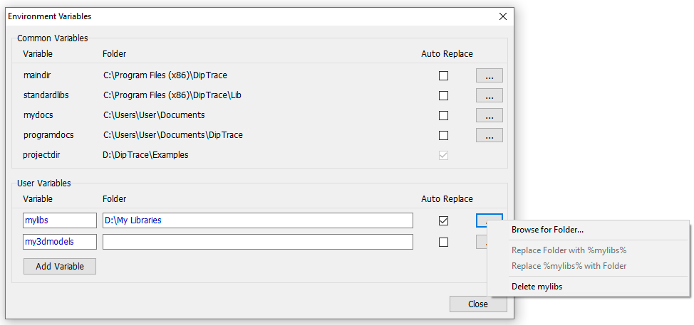
You can check the Auto Replace option for the software to substitute the path with the variable in any items with such path as soon as they appear in the project or press button and select “Replace folder with %variable name%” to apply this command to all currently existing items in the project. To reverse the command select “Replace %variable name% with Folder” from the menu.
Remember to use the same variables to set the paths to the corresponding folders on another machine. If your component or 3D model libraries have been changed, make sure to update them in the source folder on your device.
To delete a variable press and select Delete <Variable Name>.
Environment Variables feature also allows creating a portable version of the program by establishing a variable for the launch directory, which can be stored, for instance, on a portable drive.
4.2. Working with libraries
4.2.1. General properties
In DipTrace a typical electronic component consists of schematic symbol, PCB footprint (pattern) and possibly a 3D model. All these entities represent a single component on various design stages. Component editor is the tool to create and edit components, it means drawing the schematic symbol and attaching a pattern (PCB footprint designed in the DipTrace Pattern Editor).
Components are united to component libraries (files with *.eli extension) and include all attached PCB patterns. However, patterns are also stored in the pattern libraries (files with *.lib extension) for convenience.
Each component may contain one or several schematic symbols (parts) and attached pattern (for PCB Layout). If there is no pattern in the component, you cannot convert schematic which contains this component to the PCB (except net ports).
Library has two string parameters: name and hint. Select "Library/ Name and Hint of <current library>" from the main menu to change or enter them. In the Schematic the library name is shown on the Place Component panel (10 characters max. recommended).
4.2.2. Library groups
Library groups are very easy means of organizing libraries. There are three default library groups: Components, User Components and Other Libraries (auto-generated library group for storing pattern templates and separate library files).
Press  to change active library group or open the Library Setup dialog box to create and edit library groups and connect separate libraries from files.
Press  to change move/copy/delete component libraries between the library groups.
4.2.3. Library setup
To manage the library groups, select "Library \ Library Setup" from the main menu or press and select Library Setup from the submenu.
It's possible to create as many library groups as needed and add/delete libraries to the groups in the Library Setup dialog box regardless of their type and active DipTrace module. The Library Setup dialog box is the same in the Schematic, PCB Layout and other DipTrace software modules.
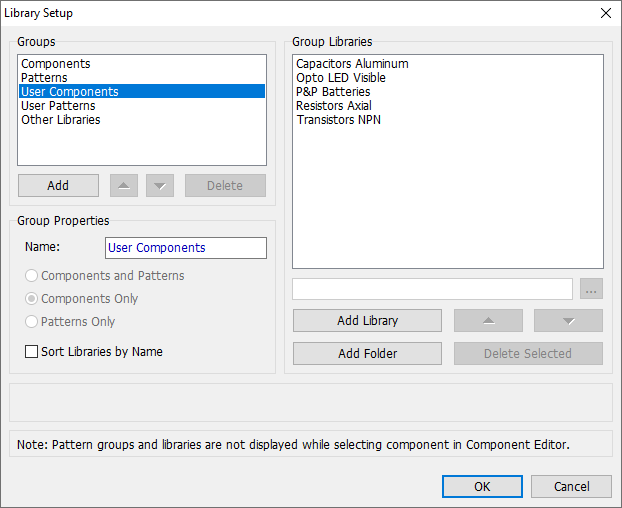
Press Add to add new library group, type in the name into the field below and select the group type, depending on what libraries you are going to store in this group. Components Only allows for adding only component libraries (*.eli files) to the group, Patterns Only – only patterns (*.lib files), Components and Patterns – both.
To add new library to the library group, press Add Library or Add Folder buttons and select the library directly from the file on your computer.
The user can not edit the standard library groups: Components and Patterns library groups.
4.2.4. Create
When you launch the Component Editor (no command prompt), the last edited library is opened by default.
To create a new library, select "Library/ New" from the main menu or press the corresponding button on the Standard toolbar or Library Manager panel. Library group for the library should be defined. DipTrace offers User Components library group by default, but you can select another library group.
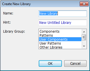
Go to Library Setup to create and manage library groups.
If current library is not saved and you try to create another library, the program will offer to save current library first. Notice that DipTrace does not allow you to modify standard libraries and library groups.
4.2.5. Open
To open a certain library, select it on the Library Manager panel. If library is not connected with DipTrace, select "Library/ Open" from the main menu or press the corresponding button on the Standard toolbar and select required component library file (*.eli). Library will be automatically added to Other Libraries library group. Use Library Setup dialog box to add this library to other library groups.
4.2.6. Save
There are two items for saving a library in the main menu: "Library \ Save" and "Library \ Save as". For the first one there is a corresponding tool on the Standard toolbar.
Select "Library \ Save" from the main menu or press the corresponding button on the Standard toolbar to save changes. If component library has never been saved, DipTrace will offer to create a new file for it. "Documents\DipTrace\My Libraries" is default folder for custom libraries. DipTrace does not allow for modifying standard libraries or saving new libraries in the "DipTrace\Libraries" folder or in the Components library group.
To save library into different file, for example, for backup, select "Library \ Save As" from the main menu.
4.2.7. Bulk Update of Patterns
To perform a bulk update of the patterns attached to the components of a certain library/-ies, go to Tools/ Bulk Update of Patterns. In the pop-up press button in the Component Library Folder section to browse for the directory that contains the component library/-ies you want to update (.eli).
Tick Make Reserve Copy of Component Libraries for DipTrace to create a copy of the library/-ies being updated in a separate folder of the original directory. We strongly recommend saving a copy of component libraries before updating them or using this option for backup.
Press button in the Pattern Library Folder section to select the directory with the library containing new patterns that will be used to substitute the current ones. Note that substitution will be performed by pattern name.
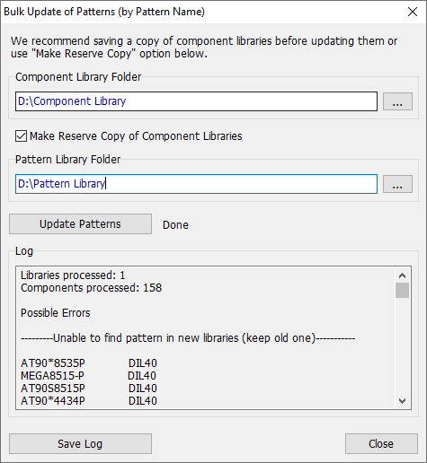
In the Log list you can check the results and see any possible errors. Press Save Log button to save the report on your computer.
4.2.8. Templates
It is much easier to create components using templates. When creating a new component, just select an appropriate existing component from the Template drop-down list on the Component properties panel to use it as an example.
To edit a template library, select "Library \ Open Templates" from the main menu or select Component Templates library in the Other Libraries group on the Library Manager panel. You can add/edit/delete components to/from the Templates library. To save a library as a template library, select "Library/ Save Templates" from the main menu.
4.2.9. Search components
To open the Search Components dialog box, select "Component/ Find Component" from the main menu.
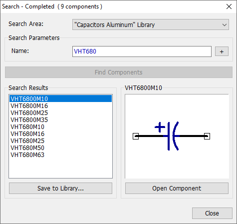
In the pop-up dialog box, select a search area (active library, library group, or all libraries).
Specify the name or part of the component's or pattern's name as well as other attributes (Value, RefDes, Pattern, Manufacturer, Additional Fields, Datasheet). Press the + button to add new search filter and use the drop-down list to set up additional search parameter.
Click Find Components to start searching. Results will appear in the corresponding list (preview available).
Press Save to Library in order to save component in the new library. Press Open Component – the library which contains selected component will be opened automatically and the component you've been looking for will be selected.
4.2.10. Search at SnapEDA
To look for the required components in SnapEDA libraries, go to "Component \ Search Parts at SnapEDA". In the pop-up, register or log-in, if necessary, then enter data in the Search field and press  button.
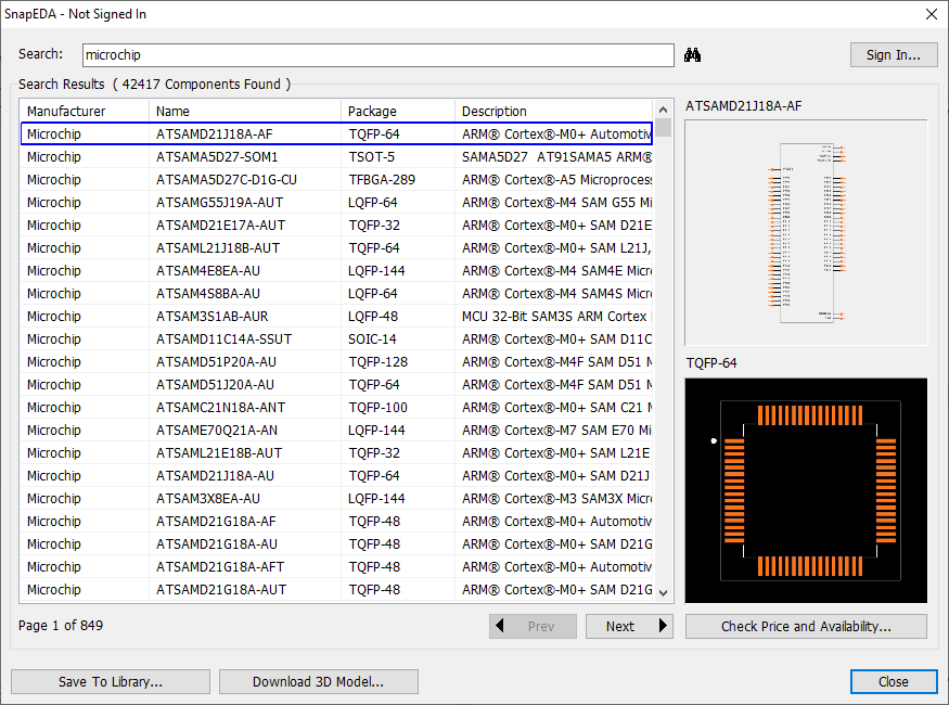
Select a component from the search results, its symbol and pattern will appear in the preview field, if available.
Press Save to Library button to add the component to the existing user library or to a newly-created one.
Download 3D Model button gets active, if a 3D model is available for the selected component. Press it to download the .step file to your computer. The model will be automatically attached to the respective pattern.
4.2.11. Working with components
There are the following functions that help work with components in the library:
Add – add new component to the library. Select "Component \ Add New to <current library>" from the main menu or press Ctrl+Ins.
Delete – delete current component from the library. Select "Component \ Delete from Library" from the main menu or press Ctrl+Del.
Insert – insert new component into current position. Select "Component \ Insert New to <current library>" from the main menu or press Ctrl+I.
Move Up – move current component up in the library. Select "Component \ Move Up" from the main menu or press Ctrl+U.
Move Down – move current component down in the library. Select "Component \ Move Down" from the main menu or press Ctrl+D.
Clear Component – delete all pins, shapes and text objects of the component. Select "Component \ Clear <current component>" from the main menu.
Insert from Another Library – allows you to get a component from another component library into current position. Choose "Component \ Insert from Another Library" from the main menu or right click on the position in the Component list and choose Insert Components from Another Library. In the pop-up dialog box select a library and component (use Ctrl and Shift for multiple selection of components). Then press Insert. You can also hold the left mouse button to select a group of components.
Deleting component/a group of components from the library – select components in the Component list (move mouse to the first component, hold down the left mouse button, move the mouse arrow to the last component and release it), then right click on the Component list and choose Delete Component from the submenu.
Duplicating components – select component in the list of components. Right click it and choose Duplicate Components from the submenu. The copy of component will appear right below the original one.
Sorting components – it is possible to sort components by name inside the library. Select "Library \ Sort Components in <current library>" from the main menu.
All these functions can be accessed directly on the Library Manager panel by pressing Component Tools and Library Tools buttons.
4.2.12. Verification
With Component Editor you can see the total number of components, parts and pins in current library and check it for possible design errors.
To open the library verification dialog box, select "Library/ Check <current library>" from the main menu.
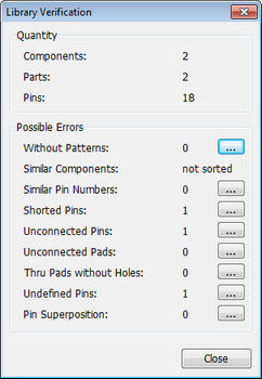
The following errors are the most common:
1. Components without patterns – search components without patterns. Keep in mind that some components may have only schematic symbol intentionally.
2. Similar components – search components with similar names. Notice that library should be sorted ("Library \ Sort Components in <current library>" from the main menu) to enable correct verification.
3. Similar pin numbers – two or more pins have similar numbers (connected to the same pad). This is probably a mistake in the component, please press the ... button and check pin numbers for the listed component.
4. Shorted pins – pins are shorted by internal pad-to-pad connections. It's not always an error.
5. Unconnected pins – pins do not have the corresponding pattern pads. It's not always an error.
6. Unconnected pads – some pads of the pattern are not used (no corresponding pins). It is not always an error.
7. Through pads without holes – verifies components for the through pads without a hole. In majority of cases this is a mistake in SMD pattern, please check if pads do really have the surface type selected.
8. Undefined pins – some pins have "Undefined" electric property.
9. Pin superposition - some pins superimpose on the symbol, in majority of cases this is a mistake made while placing the pins.
To see details of an error (list of components and pins) press ... button next to the corresponding error. You can save the list of errors to the text file and then correct the library according to that file.
4.2.13. Import/Export
4.2.13.1. DipTrace ASCII import
DipTrace allows you to save/open data in the textual DipTrace ASCII format. This format has been developed to allow for data transferring from/to other EDA packages and for forward compatibility between the DipTrace versions.
To import DipTrace ASCII-formatted library file, select "Library \ Import \ DipTrace ASCII" then select file, and click OK.
4.2.13.2. DipTrace XML import
DipTrace Component Editor allows saving/ opening data in the textual DipTrace XML format. This format can be used for data transferring from/to other EDA packages and for forward compatibility between the DipTrace versions.
To import a library file in DipTrace XML format, select "Library/ Import/ DipXML" then select file, and click OK.
4.2.13.3. Eagle import
There are two ways to import component libraries from EAGLE: Eagle Script and EAGLE XML formats.
EAGLE XML Import (recommended)
Select "Library \ Import \ EAGLE XML" from the main menu in the Component Editor and select an EAGLE library file (*.lbr) that you want to import.
EAGLE Script import
To create a script file, launch EAGLE software, select "Library \ Export \ Script" from the main menu. Save EAGLE library as an *.scr file. Now close EAGLE and open DipTrace Component Editor, select "Library \ Import \ Eagle Script (*.scr)" from the main menu and select that *.scr file.
4.2.13.4. EasyEDA Pro
DipTrace supports importing libraries from the EasyEDA Pro format (*.epro).
To import, choose "Library \ Import \ EasyEDA Pro" from the main menu in the DipTrace Component Editor, then select the desired EasyEDA Pro Project file (*.epro).
In the pop-up dialog, enter the Library Name and Hint, and select a Library Group for the imported library. Click OK to complete the import.
4.2.13.5. P-CAD import
DipTrace allows the user to import component libraries from P-CAD, using P-CAD ASCII format (*.lia).
To create ASCII library in P-CAD open the Library Executive, select "Library \ Translate", and select From: P-CAD Binary, To: P-CAD ASCII in the pop-up dialog box, then specify the library file, and press Translate.
Now close P-CAD Library Executive and open DipTrace Component Editor, select "Library \ Import \ P-CAD ASCII (*.lia)" from the main menu and open the *.lia file saved before.
4.2.13.6. Altium ASCII
DipTrace allows the user to import component libraries from Altium, using Altium ASCII format (*.lia).
Launch Altium, select schematic library, go to "File \ Save Copy As" from the main menu, select Export P-CAD V16 Schematic Library (*.lia) in the File type field and save the file. Now select PCB library and save it as Export P-CAD V16 PCB Library (*.lia). Please add custom text to the name of the files being exported to identify schematic and PCB library files (because Altium will try to give them the same names).
Now launch DipTrace Component Editor to import those files, select "Library \ Import \ Altium ASCII (*.lia)" from the main menu, select Altium schematic library, press Open, then select Altium PCB library when prompted, and press Open. Complete component library is ready, it includes schematic symbols and pattern footprints.
4.2.13.7. PADS import
DipTrace allows the user to import component libraries from PADS, using PADS ASCII format.
In PADS schematic symbols, pattern footprints and so called "logic" of a single component library are saved in separate files (*.p – parts, *.c – "logic" files, *.d – footprints), we recommend to start by importing the footprints into DipTrace.
When footprints are saved as a DipTrace library, select "Library \ Import \ PADS ASCII (*.p, *.c)" from the main menu, select a *.p-file, then import *.c-file, then select DipTrace footprint library (*.lib).
4.2.13.8. KiCAD import
DipTrace allows the user to import component libraries from KiCAD.
In DipTrace Component Editor, select "Library \ Import \ KiCAD Library (*.lib)" from the main menu and open a KiCAD library file (*.lib).
4.2.13.9. DipTrace ASCII export
DipTrace allows you to save/open data in the textual ASCII format. This format has been developed to allow for data transferring from/to other EDA packages and for forward compatibility between versions of DipTrace software.
To export library file to DipTrace ASCII format, select "Library \ Export \ DipTrace ASCII", define filename, and click OK.
4.2.13.10. DipTrace XML export
DipTrace Component Editor allows saving/ opening data in the textual DipTrace XML format. This format can be used for data transferring from/to other EDA packages and for forward compatibility between the DipTrace versions.
To export a library file in DipTrace XML format, select "Library/ Export/ DipXML" then define filename, and click OK.
4.2.13.11. Eagle XML export
DipTrace allows you to save your component library in Eagle XML format.
To export library file to Eagle XML, select "Library \ Export \ Eagle XML (*.lbr)", define filename, and click Save.
4.2.13.12. BSDL pinlist
DipTrace Component Editor allows the user to import BSDL files. This can dramatically speed-up component design process by automating some of the most time-consuming procedures. BSDL files are usually available for download at component manufacturers' websites.
Select "Library \ Import \ Add BSDL Pinlist" from the main menu. Then select file, and press Open. All pins with correct names and numbers will appear on the design area.
4.2.13.13. Pinlists
DipTrace can import pinlists in .csv and .txt formats.
To import, choose "Library \ Import \ Pinlists" from the main menu in the DipTrace Component Editor, then select one or more pinlist files.
When prompted, choose whether to add the pinlist components to the current library (Yes) or create a new library (No).
In the Import Pinlist dialog, the file columns will be displayed. Use the Column Values field to define which column contains the Pin Numbers and which contains the Pin Names.
If importing multiple files, mark Apply to All Selected Files, then click OK to complete the import.
4.3. Designing components
4.3.1. Review, properties
Component consists of schematic symbol (parts) and attached pattern (footprint). In the Component Editor you can create symbols and attach patterns from pattern libraries (*.lib files). Components are saved in the component libraries (*.eli files), patterns – in the pattern libraries (*.lib files). Patterns are created/edited in the Pattern Editor.
Schematic symbol itself consists of pins, shapes and text.
There are 15 pin types:
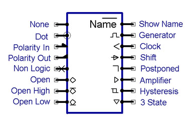
It is possible to set the Show Name parameter. To start/finish inversion use the Tilde (~) key in the name string.
To change the pin type use the pin properties dialog box or pin manager ("Component \ Pin Manager" from the main menu). To change pin parameters before placement, use the Pin Placement Setup dialog box ("Objects \ Pin Placement Setup").
There are 9 shape types: line, arc, arrow, rectangle, filled rectangle, obround, filled obround, polyline and filled polygon. Text object are also considered as shapes, but with some particular characteristics of the placement and editing.
In the Component Editor you can set the following component properties:
1. Symbol style. There are 4 symbol styles: Free, 2-sides (pins are placed on the left and right sides), IC-2 sides (pins on 2 sides of rectangle shape) and IC-4 sides (pins on 4 sides of rectangle shape).
2. Component Name.
3. Component RefDes.
4. Value (may be different for different component parts in multi-part components).
5. Manufacturer.
6. Datasheet.
7. Part type. There are three part types: Net Port, Normal and Power and Gnd. Component can contain only one part of Power and Gnd type. This part can be hidden in the Schematic by using Hide Power and Gnd function.
8. Part name. Similar parts are united by this property.
All properties can be changed on the Component Properties panel.
4.3.2. Additional fields
Components usually have 5 standard fields (Name, RefDes, Value, Manufacturer and Datasheet) and may include unlimited number of additional fields.
There are 2 types of additional fields: Text and Link. Texts may contain any textual information and can be used in the same way as standard fields in the Schematic module. Links may include links to websites. In the Schematic module right click on the component, and select Links to open any of the component links in default web browser.
To add/change default additional fields that will be added to all existing and future components, or only to all newly-created components, select "Component/ Default Additional Fields" from the main menu.
To edit/change additional fields of current component, click Additional Fields button on the Component Properties panel.
4.3.3. Pins
4.3.3.1. Create
There are 3 ways to create pins:
1. The easiest way to create an IC component is to select the corresponding symbol type on the Component properties panel and define the number of pins and the size of the graphics.
2. Place pins manually (with the mouse). Select the pin placement tool (single, pin line, pin rectangle or pin circle) from the main menu ("Objects/ Place Pins") or on the Objects toolbar, and specify pin coordinates (for single pin only) or key points of the pin shape. Pin-to-pin spacing and pin type can be predefined in the Pin Placement setup dialog box, select "Objects/ Pin Placement Setup" from the main menu.
3. Precise placement. Select "Objects/ Precise Pin Placement" from the main menu.
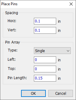
In the pop-up dialog box define pin-to-pin spacing, pin shape type (single, line, rectangle or circle), pin length, top and left point coordinates, horizontal and vertical number of pins, and press OK.
4.3.3.2. Edit
There are following functions for pin editing:
Moving – change pin position (selected pins and shapes). Drag and drop symbol to another position in the default mode.
Aligning objects – select several objects, right click on one of them and align objects respectively to each other.
Rotation – rotate pin 90 degrees counter-clockwise. Right click it and select Rotate from the submenu or select pin, and press R or Space hotkeys.
Deleting – right click it and select Delete from the submenu or select pin and press Del key.
Lines of pins can be selected and then rotated (Shift+R) or flipped (Shift+F) as single objects.
4.3.3.3. Properties
To change pin properties, right click it, and select Pin Properties from the submenu.
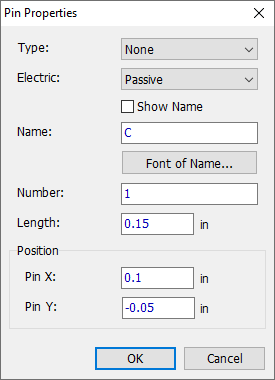
In the pop-up dialog box you can change the pin type, electric type (used for ERC), Show Name parameter, pin name, number, length and coordinates. Pin number is used to connect symbol's pins and pattern pads (pin number usually corresponds to pad number).
There are following pin types:
It is possible to show the name of the pin. To start/finish inversion in the name string use the Tilde (~) key.
To change the pin name, right click on the pin, and select Pin Name from the submenu.
Use Pin Manager for bulk changes in the pin properties.
4.3.3.4. Pin array names
Pin array naming allows the designer to name buses or several pins with similar names in a moment. Select pins, right click on one of them, and choose Pin Array Names from the submenu. The following dialog box pops up:
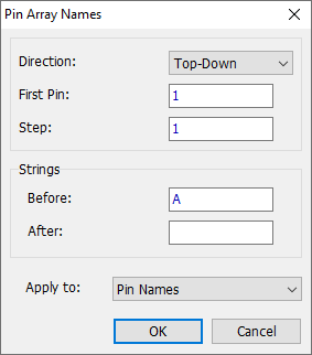
Here you can select the direction for pin naming and how to name them. The items of the drop-down list depend on the selected pins, the following directions are possible: Top – Down, Bottom – Up, Left – Right, and Right – Left.
The picture above shows naming for "A" bus with "1" step starting from A1 from the top pin. Selected pins are placed as a vertical line, therefore only Top – Down and Bottom – Up directions are possible.
Naming can be applied to the pin names or pin numbers.
4.3.3.5. Pin placement setup
Pin Placement Setup allows the user to define default parameters of pins before placing them on the design area. Type, length, spacings by axes (for multiple pin placement options), show/hide pin parameters are available. Select "Objects/ Pin Placement Setup" from the main menu.
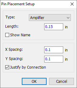
4.3.4. Shapes
4.3.4.1. Create
The following shape types are available: Line, Arc, Arrow, Rectangle, Filled Rectangle, Obround, Filled Obround, Polyline, Polygon.
There are two ways to create a shape object of the symbol:
1. Place shape with the mouse, select the Shape Placement tool from the main menu ("Objects \ Place Shape") or press the corresponding button on the Objects toolbar, and specify the key points on the design area.
To place a Line, press  button on the Objects Toolbar and select
  . Left-click to anchor the starting point and the end point. When drawing the line, it’s dimensions will be displayed by DipTrace.
To place an Arc, press button on the Objects Toolbar and select  . There are three modes for Arc placement in DipTrace. Left-click to anchor the starting point, then right-click to select placement mode:
| § | Start - Center - Angle - with this mode selected an arc with a certain angle is built based on a circle with defined radius. Anchor the starting point, the center point of a circle will appear; the radius of the circle is equal to the distance between the starting point and the center point. Move the center point away from the starting point to get a circle with desired parameters. Next left-click and adjust the angle of the arc. Left-click to anchor the end point of the arc. |
| § | Start - End - Radius - in this mode an arc of desired radius is built between the Start and End points. Place the Start and End Points and move the mouse pointer to adjust the radius of the arc. Left-click when done. |
| § | Start - End - Middle Point - in this mode an arc is built based on three points. Place Start and End point, the third point will appear on the line between them. Move the point to get an arc with desired parameters. |
Choose Clockwise or Counter-Clockwise from the right-click submenu to define the concavity direction of the curve.
Select Cancel from the right-click submenu to cancel the arc placement.
When drawing an arc, it’s key parameters (radius, deg.) will be displayed by DipTrace.
To place an Arrow, press  button on the Objects Toolbar. Left-click to anchor the starting point and the end point. When drawing the arrow, it’s dimensions will be displayed by DipTrace.
To place a Rectangle/ Filled Rectangle, press  or
or  button respectively on the Objects Toolbar. Left-click to anchor the starting point, draw the shape and left-click in the end point. When drawing the shape, it’s dimensions will be displayed by DipTrace.
To place a Obround/ Filled Obround shape, press  or
or  button respectively on the Objects Toolbar. Left-click to anchor the starting point, draw the shape and left-click in the end point. When drawing the shape, it’s dimensions will be displayed by DipTrace.
To place a Polyline/ Polygon, press  or
or  button respectively on the Objects Toolbar. Left-click to anchor the starting point, draw the shape, left-click to anchor points, right-click in the end point and select Enter form the submenu. When drawing the shape, it’s dimensions will be displayed by DipTrace.
2. Precise Placement, select "Objects \ Precise Shape Placement" from the main menu, select shape type, its key points or dimensions and press OK.
To place text, select the Text Placement tool on the Objects toolbar, click in the symbol design area, and enter the text.
4.3.4.2. Edit
There are the following functions to edit shapes:
Moving – move cursor and drag object to change shape or text position in the default mode. All selected objects will move. If you try to drag the key point of the shape, only this key point will move and the shape size will change.
Changing the size – move the mouse cursor to the key point of the shape and drag it to a new position.
Aligning objects – select several objects, right click on one of them and align objects respective to each other.
Rotation – rotate shape 90 degrees counter-clockwise. Right click on the shape, and select Rotate from the submenu or select shape and press R. All selected objects will be rotated.
Deleting – right click on the shape, and select Delete from the submenu or left-click it, and press Del key. All selected objects will be deleted.
For precise shape editing, use the Shape Properties dialog box.
4.3.4.3. Properties
Right-click on a shape, and select Properties from the submenu to open Shape Properties dialog box.
|
|
|
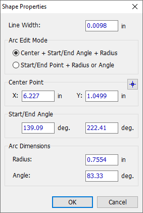
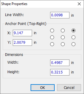
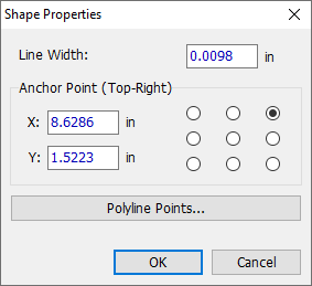
The dialog varies, depending on the shape and allows to adjust the following parameters:
Line Width: use default line width or set a new value for the given shape.
Start and End Points: can be adjusted for a line and arrow shapes by changing X and Y coordinates or by using  button to set them by Mouse Pointer.
Arc Edit mode: Center+Start/End Angle+Radius or Start/ End Point+Radius or angle. Type-in all the required values. Note that points can be defined by X and Y coordinates or set by Mouse Pointer upon pressing .
Anchor Point: change the position of an anchor point and type-in its coordinates for precise shape positioning.
Dimensions: type-in the necessary values to define shape Width and Height or Horizontal (dX) and Vertical (dY) tangent.
Polyline Points/ Polygon Points: edit dimensions of a polyline or a polygon shape.
4.3.5. Text
4.3.5.1. Create
A multiline text can be placed in DipTrace. Go to Objects/ Place Text or press button on Objects toolbar.
Left-click on the design area and type the text.
Use Enter key to move to the next line.
Right-click on a free spot of the design area to return to default mode.
Font type and size of the text can be changed upon placing it on the design area.
Note that tilde (~) before and after text is reserved by the software for placing a line over the pin name, which implies inversion; if you want a tilde symbol to appear as it is, you should place it twice:
~text~/~~text

4.3.5.2. Edit
To edit, double click on the text object or right-click on it and select Edit Text. The following dialog will appear:
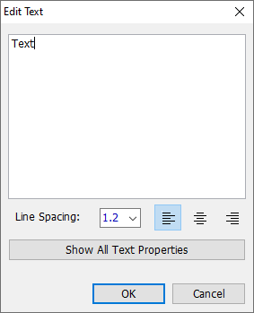
Here you can change the text, line spacing and alignment. Press Show All Text Properties button to access Text Properties dialog that allows for adjusting more text object parameters.
Right-click on a text object and select Font Type from the submenu. Vector and TrueType fonts are available. Vector font is recommended, if you use Latin characters. Unicode characters are supported only by the TrueType fonts.
To change text object size, select it and drag its key points with the left mouse button, the font size will change automatically.
Select Rotate from the text right-click submenu to rotate it at 90-degree step counter-clockwise. You can use R or Space hotkeys for the same purpose.
The user can select several component attributes to be shown in the text field (Show/ <Item> in the text submenu); this text will be automatically changed every time the respective component field is edited (Name, RefDes, Value, Part, Manufacturer, Datasheet).
Aligning objects – select several objects, right click on one of them and align objects respective to each other.
Deleting – right click on the shape, and select Delete from the submenu or left-click it, and press Del key. All the selected objects will be deleted.
4.3.5.3. Properties
To open Text Properties dialog, right-click on the text object and select Properties from the submenu.
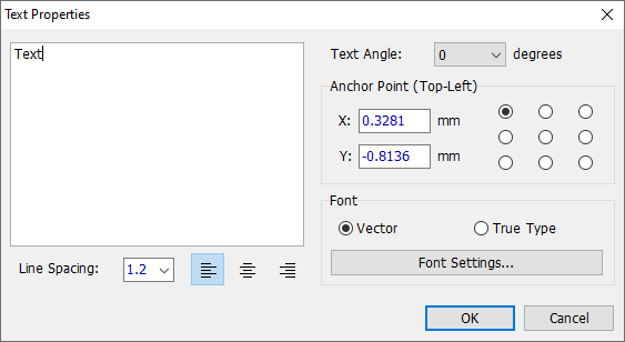
In the pop-up dialogue you can set line spacing and text alignment.
Choose an angle from the Text Angle drop-down or just type-in the required value to rotate the text.
The location of the Anchor Point of the text box is set by ticking the respective circle. Anchor Point is displayed as a cross. You can also set the coordinates of the Anchor point for precise text positioning.
Select Font Type: Vector font is recommended, if you use Latin characters; unicode characters are supported only by the TrueType fonts.
Press Font Settings button to open Font dialog (it can also be accessed by selecting Font in the text right-click submenu):
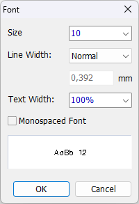
Here you can set the font size, select the Line Width from Thin, Normal, Bold or Customize it, and also define the Text Width.
Mark Monospaced Font to distribute character spacing evenly across the text, applicable to vector font only.
4.3.6. Multi-part component
4.3.6.1. Working with parts
DipTrace allows the user to create multi-part components.
There are 3 part types: Normal, Power and Gnd, and Net Port. Component can contain only one part with Power and Gnd type. This part can be hidden in the Schematic with Hide Power and GND feature. Net Port components (parts) are used to connect wires without visual connection (they can be used for VCC, GND, etc.). Change part type with a drop-down list on the Component Properties panel.
All parts of the multi-part component appear in the bottom-left corner of the symbol design area as tabs:

Add a new part – select "Component \ Add New Part" from the main menu.
Insert a new part (before current part) – select "Component \ Insert New Part" from the main menu.
Delete current part – select "Component \ Delete Current Part" from the main menu.
Component can contain similar parts, which are absolutely identical, except the pin numbers (pin-to-pad connections).
To create similar parts based on current part, select "Component \ Create Similar Parts" from the main menu, enter the number of parts added, and press OK.
4.3.6.2. Similar parts
Component can contain similar parts. They are absolutely identical, except for the pin numbers (pin-to-pad connections).
To create similar parts, based on current part, select "Component \ Create Similar Parts" from the main menu, enter the number of parts, and press OK.
Similar parts are united by the part name. If you edit one part, all similar parts will change automatically (except the pin numbers).
There are two modes of how multi-part components are shown in the Schematic: single part or each part separately. If similar parts are shown by a single item, the part to place is selected automatically, depending on existing parts already on the design area ("View \ Group Similar Parts" from the main menu in the DipTrace Schematic).
The number of similar part groups in the component is unlimited.
4.3.7. Aligning objects
Select objects on the design area, then go to "Edit/ Align Objects" from the main menu, or right click on one of the objects and select Align Objects from the submenu.
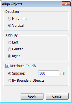
Select the alignment direction, then select how to align objects in the row or column (left, center or right) and set distribution settings by objects' boundaries or equally with a custom spacing.
You need to select at least two objects to have the Align tool available, because the alignment is relative.
4.3.8. Edit component
General editing functions for the component's symbol:
Center symbol with respect to zero point (coordinates). Select "Edit \ Center Symbol" from the main menu or press Ctrl+Alt+C.
Rotate symbol 90-degrees clockwise with respect to the zero point. Select "Edit \ Rotate Symbol" from the main menu or press Ctrl+Alt+R.
Flip symbol vertically with respect to "X" axis. Select "Edit \ Vertical Flip" from the main menu or press Ctrl+Alt+V.
Flip symbol horizontally with respect to "Y" axis. Select "Edit \ Horizontal Flip" from the main menu or press Ctrl+Alt+H.
4.3.9. Changing the symbol style
It is possible to change the symbol style (Free, 2-sides, IC-2 sides, IC-4 sides) without losing existing pins and shapes. Then you will be able to edit the symbol regarding its new style (change width and height).
To change the symbol style, select "Component \ Change Symbol Style" from the main menu, and specify a new style.
This can be applied to old symbols created with Free style if you need to change width/height, sort pins, make buses, etc.
4.3.10. Pad signal delay
Bond wires inside electronic component's package connect pads to the die. These wires introduce a signal delay which should be accounted for in high-speed designs. Manufacturers report this in-device pad signal delay in picosecond time or as a length in the datasheets. Pad signal delay value is considered for phase and length tuning and is added to the total length of the tracks when on the circuit board.
To set pad signal delay in the Component Editor, select "Component \ Pad Signal Delay" from the main menu.
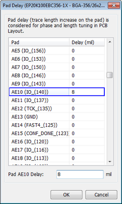
Select pad from the list and enter the signal delay in mils right below. Press OK to apply changes. Pad Delay dialog box is also available from the Pin Manager in the Component Editor. You can also assign pad signal delays on the schematic and PCB design stages.
4.3.11. Making buses, pin positioning
Once you entered all pin names and numbers in the Pin Manager, you probably may need to make buses and place pins in some order.
Component Editor has 2 special tools to achieve that:
1. IC Pin Repositioning – this tool sorts pins by pin names (alphabetically) or by pin numbers, then locates pins according to the new order and order/direction settings. Select "Component \ IC Pin Repositioning" from the main menu to launch the pin repositioning, and "Component \ IC Pin Repositioning \ Order and Direction Settings" to customize order and direction of repositioning.
2. Making Buses – this tool sorts pins to buses by pin names and places them to the left from the symbol. Select "Component \ Make Buses from Pins" from the main menu. In the pop-up dialog box, define possible bus dividers, and press Extract button.
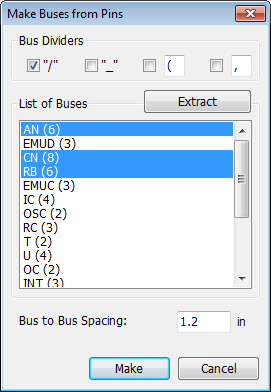
Now you can see the buses and the number of pins in each of them (listed in the brackets). Select buses that you need to place (use Ctrl or Shift keys) for multiple selection, and press Make button. Bus pins will be sorted by number in the bus and placed to the left from the symbol in different columns. Then you can place them to the symbol sides manually.
Use Shift+R to rotate bus and Shift+F to flip the bus pins.
4.3.12. Attached pattern
To create a complete component, you should attach pattern to the symbol and define pin-to-pad connections. Select "Component \ Attached Pattern" from the main menu or press the Pattern button on the Component Properties panel.
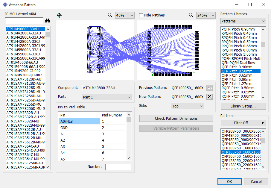
In the pop-up dialog box, you can see the list of all components of current library to the left with current component selected. Pattern for the component should be selected from the Pattern Libraries list. Change active Library Group (if needed), select library, then select a pattern. Use search filters for convenience. Press Library Setup to edit library groups.
When pattern is selected, it appears in the preview area and DipTrace assigns pin-to-pad connections. Review and change them in the Pin to Pad table or visually in the symbol and pattern preview fields.
1. Visually – left-click on the pin, then left-click on the pad – the connection line will appear. To delete connection, right click on the corresponding pin or pad. All connections are shown in the connection list (in the bottom-left corner of the dialog box).
Notice that it is possible to connect one pin to two footprint pads, just create an internal connection between the pattern pads: left-click on a pad and then click on another one, with which you want to create a connection - a menu will pop up; confirm or cancel pad connection by selecting the respective option.
2. Pin to Pad List – select pin from the list and enter pin number (pad number) into the Number field below. Note that pads with the same numbers are automatically connected to one net. Use @ sign after the identical pad numbers to avoid errors.
However, the Pin Manager is the most convenient way to define pin numbers (pin-to-pad connections).
The designer can Undo to the previous pattern if his new choice is not appropriate or delete the pattern.
Side option is good for SMD patterns with pads on both sides of the board (for example, edge connectors).
If it is a multi-part component, each part can be selected separately in order to define the pin numbers.
4.3.13. SPICE Model
To define/edit the component SPICE settings, select "Component\ SPICE Model" from the main menu. The following panel will appear:
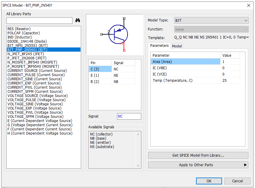
All the parts of the current library are displayed on the left. Left-click to select the required component from the list or use the search field to find it.
Pin-to-signal connections can be established using the table in the central part of the dialog box. The list of available signals with comments is located right below.
The dialog allows selecting the model type, defining parameters, model and signals for the components.
Resistor, Capacitor, Inductor, Sources, Mutual Inductance and Transmission Line types do not require models and you can define their parameters manually. SubSkt type is often used to define logics, chips, etc., however, it can be used for almost any purpose.
Notice that models can be loaded from external ASCII files (usually available at manufacturers' websites or other locations on the Internet), just select the Model tab and press Load.
A SPICE model can also be loaded from the existing DipTrace library (press Get SPICE Model from Library button and select the respective Library group, Library and Component).
Once defined, component SPICE settings can be applied to Similar parts of the Component or All Similar Parts of the Library - press the Apply to Other Parts button and select the required option.
Template line shows how the component will be displayed in the Spice netlist. Notice that you can scroll it to the right if necessary, because templates are quite long.
If you are not familiar with SPICE language, we recommend using SPICE Language Documentation available on the Internet to discover more details.
4.3.14. Pin Manager
Pin manager is a great tool to add or delete pins, change name, number, type, coordinates of pins, etc.
To open the Pin Manager, select "Component \ Pin Manager" from the main menu.
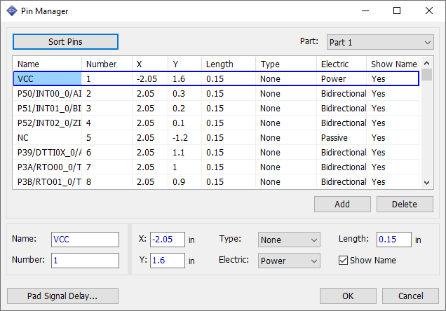
To change pin properties, select pin from the table and change its properties in the corresponding fields below.
It is possible to select several pins at a time and change their pin and electric types, the Show Name parameter and the length.
Pin number defines pin-to-pad connections (actually it is the number of related pad), thus you can change pin-to-pad connection by changing the corresponding pin numbers.
Press Pad Signal Delay to set signal delays on the component pads.
If component contains several parts, each part has its own pin table. To change current part, use the Part drop-down box in the upper-right. To add new pin to the table press Add button. To delete selected pins, press Delete button.
Pins can be easily sorted by name, number or location in the component.
Pin Manager panel can be resized if necessary.
4.3.15. Insert from library
To get component from the component library, select "Component/ Insert from Another Library".
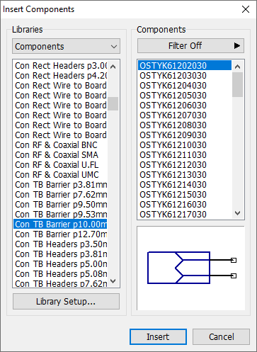
In the pop-up dialog box select the library group, then select library and it's component. Use search filters if needed. Library Setup and symbol's preview fields are available.
4.4. View functions
4.4.1. Scaling/Panning
There are several ways to change the scale of design area:
1. Mouse wheel – you can decrease or increase the scale in very wide limits.
2. Drop-down list on the Standard toolbar (from 25% to 800%).
3. "View \ Scale" from the main menu. It is possible to select from 25% to 800%, zoom in, zoom out or specify custom scale.
4. Pressing the Plus sign (+) key to zoom in or Minus sign (-) key to zoom out.
5. Zoom window tool on the Standard toolbar allows for zooming to the box defined with the mouse pointer.
Current scale is always displayed in the drop-down list on the Standard toolbar.
Pan design area with the right mouse button (hold down and move) or by arrow keys while creating the shape etc.
4.4.2. Grid
DipTrace Component Editor allows the user to create and edit objects free or according to the grid.
To show/hide the grid, select "View \ Grid" from the main menu or press F11 hotkey.
Select "View \ Snap to Grid" from the main menu, or press Alt+F11 hotkey (by default) to activate/deactivate snap to grid, when the grid is on.
If Snap to Grid option is disabled, objects are no longer snapped to the grid, but you can leave the grid visible.
When Snap to Grid option is disabled for the entire project, you can choose to snap to grid individual elements of your pattern (pad, shape, text, image, etc.) by selecting Snap to Grid item from the right-click submenu of those elements, when the grid is on.
Select "View \ Grid Size" from the main menu to open the grid size submenu. You can select standard or specify custom grid size.
It is possible to select grid size from the list on the Standard toolbar or just press Ctrl + Plus sign (+), Ctrl + Minus sign(-) hotkeys to change the grid.
To change the list of predefined grid sizes, select "View \ Customize Grid" from the main menu.
4.4.3. Origin
Origin is customizable, you can change its position at any moment while creating and editing a component. Select "View \ Display Origin" from the main menu or press F1 hotkey.
Origin can be defined with the mouse pointer or by coordinates (incremental to existing origin). To define it with the mouse, select "View \ Define Origin \ By Mouse Pointer" from the main menu or press the corresponding button on the Objects toolbar, then define a new origin with a left-click on the design area. To change the origin by coordinates, select "View \ Define Origin \ By Coordinates" from the main menu.
To return origin to default position (center of the design area) select "View \ Define Origin \ Default Position".
To change the color of the axis, select "View \ Axis Color" from the main menu.
4.4.4. Pin numbers
To show/hide pin numbers for the component, select "Component \ Pin Numbers" from the main menu and select one of three states: Show – show part pin numbers, Hide – hide part pin numbers, Default – use default settings. This should be assigned before part placement in the Schematic module.
To change default settings, select "View \ Pin Numbers" from the main menu.
To change position of pin numbers and pin names, select "View \ Move Text Tool" from the main menu or press F10 hotkey and move texts visually.
4.5. Edit functions
4.5.1. Select objects
You need to select objects before editing or removing them. DipTrace has several ways to select objects or to edit existing selection:
1. Click on the object with any of the mouse buttons. Use left mouse button to select object (hold down the left mouse button to move it) and the right mouse button to select object and open its submenu with different options, settings and tools. Notice that you can select overlapping objects with several left-clicks, in this case you will be able to move or open the submenu for selected object.
2. In the Default mode hold down the left mouse button on an empty area and start moving the mouse cursor – selection box will appear. All objects inside this box will be selected when you release the mouse button.
To invert object selection, press Ctrl key and select objects. To add objects to the selection use Shift key.
To select all symbol objects, choose "Edit \ Select All" from the main menu.
3. Edit Selection dialog box allows the user to select objects by type. Different modes are supported: new selection, add to selection, remove from selection, keep selected. Choose "Edit \ Edit Selection" from the main menu.
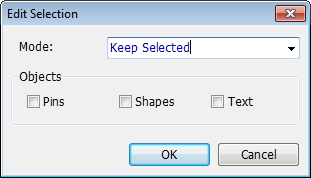
In the pop-up dialog box select objects with the corresponding check boxes and select the mode:
1. New Selection – automatically deselect all previously selected objects and create a new selection, based on your choice;
2. Add to Selection – add specified objects to existing selection;
3. Remove from Selection – remove specified objects from existing selection;
4. Keep Selected – deselect objects which are not specified. This mode allows for selecting objects by type and area. For example, use box selection and Ctrl (see above) to define selection area, all objects in this area will be selected. Now select Keep Selected mode to remove unnecessary objects from the selection.
4.5.2. General functions
There are the following general editing functions: Delete, Cut, Copy, and Paste.
Select objects before applying these functions.
To apply one of these functions to objects, select the corresponding sub-item from the main menu ("Edit"). It is possible to use hotkeys: Cut (Ctrl+X), Copy (Ctrl+C), Paste (Ctrl+V), and Delete (Del).
4.5.3. Undo/Redo function
To cancel the last editing step and return to the previous state, select "Edit \ Undo" from the main menu or press the corresponding button on the Standard toolbar.
It is also possible to recover canceled steps. Choose "Edit \ Redo" from the main menu or press the corresponding button on the Standard toolbar. If you edit symbol after using the Undo tool, Redo tool becomes inactive.
4.5.4. Move/Rotate objects
To change location of some objects select them, and drag to a new location.
You can use the arrow keys to move selected objects. Hold down the Shift key for orthogonal moving. To rotate objects counter-clockwise, select them first, then press R key or select "Edit \ Rotate" from the main menu.
Lines of pins (buses) can be selected and rotated (Shift+R) or flipped (Shift+F) as a group.
4.5.5. Align objects
Select objects on the design area, then go to "Edit \ Align Objects" from the main menu, or right click on one of the objects and select Align Objects from the submenu.
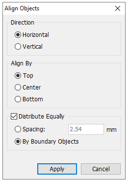
Select the alignment direction, then select how to align objects in the row or column (left, center or right) and set distribution settings by objects' boundaries or equally with a custom spacing.
You can group multiple objects into one so they will stay together if they are aligned or distributed.
At least two objects (or groups of objects) have to be selected for the Align tool to become available because the alignment is relative.
5. Pattern Editor
5.1. User interface
5.1.1. Main window
The Pattern Editor's main screen includes the pattern design area, the main menu, toolbars, Library Manager, Pattern Properties panel, pattern layers panel and the status bar.
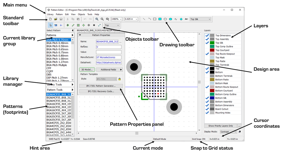
On the pattern design area you can create and edit pattern objects (pads, shapes, mounting holes, etc.).
Access to all common functions of the program via the main menu. There are the following items in the main menu: Library, Pattern, Edit, View, Objects, Tools, Help.
Other interface elements are:
Standard Toolbar – tools to work with files, cut/copy/paste objects, change scale and the grid size.
Objects Toolbar – tools to switch to the default mode, create and edit pads, mounting holes and dimensions.
Drawing Toolbar – tools to draw shapes and create texts.
Library Manager panel – pattern and pattern library management tools, sort libraries by library groups, user libraries, etc. Select library from the list and then select pattern for editing from the list right below. Set up the libraries, add/edit/delete library groups, manage search filters, verify libraries, etc.
Pattern Properties panel – all basic instruments and parameters to edit/build patterns. Templates, styles, define name, RefDes, value, datasheet, additional fields connect 3D model to the footprint and define default pad properties. The panel is located in the pattern design area. It is possible to show/hide the Pattern Properties panel or minimize it.
Layers panel – allows switching layers and managing the way the list of the layers is displayed in the current project (move/hide layers, change layer display mode). It's located on the right side of the screen. All layers or only the list of user-defined priority layers can be displayed. You can open Layer Priority and Order dialogue ( button) to select priority layers and change their order in the list. Use blue check marks to show/hide the layer, and color rectangle to change the layer color. Double-click on the layer name to make a layer active. Define Display Mode by selecting the desired option from the drop-down.
5.1.2. Toolbars
The program has three main toolbars, the Library Manager panel, Pattern Properties panel and pattern layers panel:
Standard Toolbar

This panel contains the following buttons:
New – create a new pattern library. In case the previous one was not saved, the software will offer to do this. Only one library can be opened at a time.
Open – open existing pattern library (*.lib) file. If library is not in connected yet, it will be automatically added to Other Libraries library group.
Save – save current pattern library. If library has never been saved, a special dialog box will offer to save it. If library already has the corresponding *.lib file, it will be saved automatically into that file. This tool is active only for unsaved changes.
Cut – move selected object/s to the clipboard.
Copy – copy selected object/s to the clipboard.
Paste – paste object/s from the clipboard.
Undo – one editing step backwards.
Redo – one editing step forward. It is activated after using the Undo tool. If you edit pattern after using Undo tool, the Redo becomes inactive.
Zoom Window – set current scale and pan pattern design area to the mouse-defined box.
Undo Zoom – return to the previous scale and panning.
Scale – change design area scale (from 25% to 800% or type in a new value). Changing the scale is also possible with the mouse wheel, plus sign (+) and minus sign (-) default hotkeys or from the main menu.
Grid Size – selection of current grid size from the drop-down list or by typing in a new value.
Objects Toolbar

The panel contains tools to switch to the default mode, measure distances (the ruler), define origin, create pads (single, pad line, pad rectangle, pad circle), create a mounting hole, a fiducial, place dimensions, select current side for placing objects. The number of pads to be placed, diameter of the mounting holes and some other settings depend on the parameters set in the Placement Setup dialog box.
Drawing Toolbar

The panel contains tools to create shapes and text objecys. It is also possible to select shape placement layer with a drop-down list.
Pattern Properties panel
|
This panel allows the user to change properties of the pattern. It has all necessary tools for creating a typical pattern, plus the buttons for most basic and necessary features: Attach 3D Model, Additional Fields, and Default Pad Properties.
There are 8 pattern styles: Free, IPC-7351, Circle, Lines, Square, Matrix, Rectangle and Zig-Zag. Different pattern types have different parameters. When you change the size, all shapes are resized automatically. Use this panel to define pattern name, add name description and unique name (
It is possible to create patterns, using patterns as templates.
|
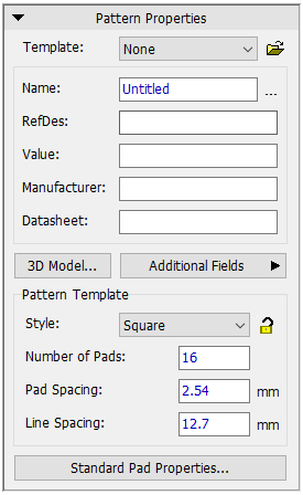
Pattern Layers panel
|
This panel allows changing layers and managing the way the list of the layers is displayed in the current project (move/hide layers, change layer display mode). It's located on the right side of the screen. The list of all layers or only of user-defined priority layers can be displayed. You can open Layer Priority and Order dialogue by clicking |
5.1.3. Library Manager panel
|
The Library Manager panel provides access to all necessary library and pattern management tools. This panel consists of two lists and three buttons.
Library list
Select library from the list and all patterns from the library will be available in the Pattern list right below.
Library Setup (add/delete libraries to/from the library groups, add/delete new library groups). Library management is cross-module – all groups and libraries customized in other DipTrace software modules (Schematic, PCB Layout, and Component Editor) will be available for editing here. Pattern Editor works only with patterns, not with components.
Pattern list
All patterns of selected library.
Hide the Library Manager by pressing a small arrow near the "Select Pattern" text. Left-click on the pattern to open it on the design area or right-click it to open the submenu with all Pattern Tools.
To adjust the width of the Library Manager panel hover over its right border and drag it. |
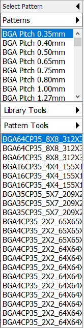
 – find patterns, insert new patterns into current library or another library, move patterns up and down the list, copy and move patterns between the libraries, duplicate and delete them.
5.1.4. Status Bar
Status bar is located in the bottommost part of the Pattern Editor window.

It shows the following information:
Hint - standard hint containing information about the selected object on the design area.
Mode - shows the current mode (Default, Place Pins, Place Shape, etc.).
Grid Snap - the current Snap to Grid status.
X, Y - coordinates of the current position of the cursor or selected element.
5.1.5. Main menu
5.1.5.1. Library
New – create a new pattern library and define its library group. DipTrace offers to create a new library in the User Patterns library group by default. If current library has unsaved changes, the program will offer to save it.
Open – open existing pattern library (*.lib or *.libxml) file.
Open Recent – last five pattern libraries.
Save – save current pattern library. If library has never been saved, a special dialog box will offer to do that. DipTrace offers to save user libraries into "Documents\DipTrace\My Libraries" folder by default. If library already has the corresponding *.lib file, it will be saved automatically into that file. This tool is active only when there are unsaved changes.
Save as – save pattern library into the file, select location and name of the file.
Import – import libraries from other formats.
Export – export libraries to other formats.
Library Setup – add/delete/copy/move libraries to/from the library groups, add/delete new library groups. Library management is cross-module, hence all groups and libraries customized in other DipTrace modules (Schematic, PCB Layout, and Component Editor) will be available for editing here.
Name and hint of <current library> – define name and hint for active library.
Sort Patterns in <current library> – sort components of current library by name.
Check <current library> – general library information (total number of patterns and pads) verification for possible errors and error report in the same dialog box.
Open Templates – open pattern templates library.
Save Templates – save current library as pattern template library.
Exit – close the Pattern Editor.
5.1.5.2. Pattern
Find Pattern – search patterns by name, datasheet, additional fields, value, manufacturer etc.
Search Parts at SnapEDA – search SnapEDA libraries directly from within DipTrace.
Add New to <current library> – add new pattern to the library.
Insert New to <current library> – insert new pattern to the library (into current position).
Insert from Another Library – insert new pattern from another pattern or component library into current position.
Duplicate Selected – duplicate selected patterns.
Import from DXF – import pattern drawing from the DXF file.
Move Up – move current pattern up in the library pattern list.
Move Down – move current pattern down in the library pattern list.
Move to the end – move current pattern to the end of the library pattern list.
Copy to Another Library – copy selected pattern to another library.
Move to Another Library – move selected pattern to another library.
Clear <current pattern> – delete all content of selected pattern.
Delete from Library – delete current pattern from the library.
Standard Pad Properties – change default pad properties for the pattern.
IPC-7351 Pattern Generator – launch Pattern Generator to create footprints and 3D models to IPC Standard based on entered parameters.
Standard Pad Mask/ Paste - define default paste and mask settings for the pads.
Standard Pin terminals – establish default pin terminal shape (obround, rectangle, polygon, D-shape); you can add and use up to 4 shapes to get the desired pin projection. Enter values to define shape size, X and Y offset relative to the pad shape and rotation angle. The settings can be applied as defaults to the Standard Pads (the ones to be placed) or All Pads (the ones already placed) of the current pattern.
Origin Properties – choose how to display the origin shape by default and whether to show it in all layers and in Courtyard layer in particular.
3D Model – attach 3D model to the pattern (required for the 3D Preview; can be attached in the PCB Layout).
Default Additional Fields – add default additional fields to be shown in pattern properties.
Some items of this menu may vary depending on the selected pattern Style.
5.1.5.3. Edit
Undo – one editing step backwards.
Redo – one editing step forward. It is activated after using the Undo tool. If you edit the pattern after using Undo tool, the Redo becomes inactive.
Cut – move selected object/s to the clipboard.
Copy – copy selected object/s to the clipboard.
Paste – paste object/s from the clipboard.
Delete – delete selected object/s.
Select All – select all objects of the pattern.
Edit Selection – selecting objects by type, layer, etc. Different modes: new selection, add to selection, remove from selection, keep selected.
Rotate – rotate selected objects 90 degrees counter-clockwise.
Rotate Group – rotate selected objects as a group.
Flip Group – flip selected objects as a group horizontally or vertically.
Align Objects – align selected object horizontally or vertically and distribute them equally.
Radial Placement – place selected objects radially with defined placement center, radius, step or distribute them equally between specified circonference angles. The feature can be applied to pads, mounting holes and fiducials.
Group – group selected objects.
Ungroup – ungroup selected objects.
Lock Selected – lock moving and editing of selected objects.
Unlock Selected – unlock moving and editing of all selected objects, if they were previously locked.
Center Pattern – center current pattern with respect to the zero point
Rotate Pattern – rotate current pattern 90 degrees clockwise with respect to the zero point.
Flip Pattern – flip current pattern horizontally or vertically with respect to the zero point.
5.1.5.4. View
Toolbars – show/hide the toolbars.
Display Hint – display standard or detailed hint (with pad/hole dimensions) for the objects on the design area. Notice that hint is always shown in the bottom-left corner of the screen.
Pattern Style Dimensions – display dimensions for the component on the design area (if pattern style was selected on the Pattern Properties panel).
Pad Numbers – show/hide the pad numbers and change their font.
Scale – change the scale. The mouse wheel or plus sign (+) and minus sign (-) hotkeys can be used to zoom in/out.
Units – change the measurement units (mm, mil or inches).
Display Side – change display mode (contrast, current side only or both). Current side can be selected with a drop-down list on the Objects toolbar. Useful tool when drawing edge connectors or other double-sided patterns.
Scale – change the scale. The mouse wheel or plus sign (+) and minus sign (-) hotkeys can be used to zoom in/out.
Line Width – set default width of the lines for shapes in different layers (Silk, Component Outline, Courtyard, Board Cutout, Other Layers).
Units – change the measurement units (mm, mil or inches).
Display Origin – show/hide the origin.
Define Origin – define the origin visually with the mouse pointer or by coordinates (incremental to existing origin point).
Axis Color – change axis color for the origin.
Grid – show/hide the grid.
Snap to grid – enable/ disable snap to grid option, when the grid is on.
Grid Size – change the grid size (standard and custom).
Y Grid Size – separate grid step for the vertical axis.
Customize Grid – edit grid sizes.
5.1.5.5. Objects
Place Pads – Place Pads submenu.
Place Shape – Place Shape submenu.
Place Text – place text object.
Place Mounting Hole – place mounting hole.
Place Fiducial – place fiducial.
Placement Setup – Placement Setup dialog box (define default pad placement settings and default mounting hole diameter).
Place Dimension – place dimensions and pointers.
Measure – the ruler tool for measuring any sizes/distances directly on the design area.
Precise Pad Placement – Place Pads by entering its parameters coordinates.
Precise Hole Placement – place mounting hole by entering its parameters coordinates.
Precise Shape Placement – Place Shape by entering its parameters coordinates.
Place Outline – automatically create pattern outline based on the outer edges of its elements; you can select outline shape type, layer and set clearances from other pattern elements.
Remove Silk from Pads – remove silk, ensuring predefined spacing from Pads, Holes and Mask Openings.
5.1.5.6. Tools
HotKey Settings – define keyboard shortcuts for dialogs and tools.
Environment Variables – define and manage environment variables.
Component Editor – launch the Component Editor.
PCB Layout – launch the PCB Layout.
Schematic – launch the Schematic.
5.1.5.7. Help
Pattern Editor Help – Pattern Editor help file.
DipTrace Tutorial – DipTrace tutorial in PDF format.
Request Support – DipTrace technical support portal.
Library Design Service – online request form for library design service (performed by experienced engineers).
DipTrace Home Page – DipTrace official website.
About – information about current version and edition.
5.1.6. Objects submenus
5.1.6.1. Pad
Right-click on any pad to open this submenu:
Pad Number – change pad number.
Pad Array Numbers – automatically rename/renumber all selected pads at a time according to selected template. For example, the BGA matrix (from A1–A30, to Y1–Y30 etc.).
Convert to Shape – convert polygonal pad to shape object for easy editing, back conversion is possible.
Lock Selected – lock moving and editing of all selected objects.
Unlock Selected – unlock moving and editing of all selected objects, if they were previously locked.
Mask/Paste Settings – custom solder mask swell and paste mask shrink settings for particular pads.
Change Side – change side of the pad (Top or Bottom).
Rotate – rotate selected objects 90 degrees counter-clockwise.
Align Objects – align selected objects horizontally or vertically and distribute them equally.
Radial Placement – place selected pads radially with defined placement center, radius, step or or distribute them equally between specified circonference angles.
Snap to Grid – snap selected pads to the grid, when the grid is on, but Snap to Grid option is disabled for the overall project.
Mask/Paste Settings – custom solder mask swell and paste mask shrink settings for particular pads.
Pin Terminal – establish pin terminal shape (obround, rectangle, polygon, D-shape); you can add and use up to 4 shapes to get the desired pin projection. Enter values to define shape size, X and Y offset relative to the pad shape and rotation angle.The settings can be applied to the Current Pad, Similar Pads, Selected Pads or All Pads of the current pattern.
Cut – move selected object/s to the clipboard.
Copy – copy selected object/s to the clipboard.
Group – group selected objects.
Delete – delete selected object/s.
Ungroup – ungroup selected objects.
Properties – change the pad properties for selected pads.
5.1.6.2. Shape
Right-click on any shape to open this submenu:
Convert to Pad – convert a polygonal shape on the signal layer to a polygonal pad.
Lock Selected – lock moving and editing of all selected objects.
Unlock Selected – unlock moving and editing of all selected objects, if they were previously locked.
Insert Point – insert point to the polyline or polygon.
Delete Point – delete point from the polyline or polygon.
Rotate – rotate selected objects 90 degrees counter-clockwise.
Align Objects – align selected objects horizontally or vertically and distribute them equally.
Snap to Grid – snap selected shape/s to the grid, when the grid is on, but Snap to Grid option is disabled for the overall project.
Cut – move selected object/s to the clipboard.
Copy – copy selected object/s to the clipboard.
Delete – delete selected object/s.
Group – group selected objects.
Ungroup – ungroup selected objects.
Properties – change shape properties.
5.1.6.3. Text
Right-click on any text object to open this submenu:
Edit text – change the text. Object size is changed automatically.
Show – change the state of the text object. It is possible to automatically display user-defined text or the Name, Unique Name, RefDes, Value, Manufacturer, Datasheet of the pattern, no need to type it in manually.
Font Type – select the font type for the text object (Vector or TrueType). Unicode is supported only in the TrueType mode.
Font – change font of the text. Text object is scaled automatically.
Lock Selected – lock moving and editing of all selected objects.
Unlock Selected – unlock moving and editing of all selected objects, if they were previously locked.
Rotate – rotate selected objects 90 degrees counter-clockwise.
Align Objects – align selected objects horizontally or vertically and distribute them equally.
Snap to grid – snap text object to the grid, when the grid is on, but Snap to Grid option is disabled for the overall project.
Cut – move selected object/s to the clipboard.
Copy – copy selected object/s to the clipboard.
Delete – delete selected object/s.
Group – group selected objects.
Ungroup – ungroup selected objects.
Properties – adjust the properties of a text object, such as line spacing, alignment, font type, layer, angle of rotation, location and coordinates of anchor point and font settings (size, line width, text width).
5.1.6.4. Mounting hole
Right-click on a mounting hole to open the submenu:
Lock Selected – lock moving and editing of all selected objects.
Unlock Selected – unlock moving and editing of all selected objects, if they were previously locked.
Rotate – rotate selected objects 90 degrees counter-clockwise.
Align Objects – align selected objects horizontally or vertically and distribute them equally.
Radial Placement – place selected objects radially with defined placement center, radius, step or or distribute them equally between specified circonference angles.
Snap to grid – snap mounting hole to the grid, when the grid is on, but Snap to Grid option is disabled for the overall project.
Cut – move selected object to the clipboard.
Copy – copy selected objects to the clipboard.
Delete – delete selected objects.
Group – group selected objects.
Ungroup – ungroup selected objects.
Properties – change mounting hole position and diameters of the Hole and Keepout.
5.1.6.5. Fiducial
Right-click on a fiducial to open the submenu:
Fiducial Name – enter fiducial name. Fiducial name is not displayed in the design area.
Lock Selected – lock moving and editing of all selected objects.
Unlock Selected – unlock moving and editing of all selected objects, if they were previously locked.
Change Side – change side of the fiducial (Top or Bottom).
Align Objects – align selected objects horizontally or vertically and distribute them equally.
Radial Placement – place selected objects radially with defined placement center, radius, step or or distribute them equally between specified circonference angles.
Snap to grid – snap fiducial to the grid, when the grid is on, but Snap to Grid option is disabled for the overall project.
Pad Mask/ Paste Settings – define custom paste and mask settings for the fiducial.
Cut – move selected object to the clipboard.
Copy – copy selected objects to the clipboard.
Delete – delete selected objects.
Group – group selected objects.
Ungroup – ungroup selected objects.
Properties – change fiducial name, position and diameters of exposed copper and keepout.
5.1.6.6. Dimensions
Right-click on dimension object on the design area to open the submenu:
Connect – connect dimension to object's key points.
Disconnect – disconnect dimension from the object's key points.
Lock Selected – lock moving and editing of selected objects.
Unlock Selected – unlock moving and editing of selected objects, if they were previously locked.
Cut – move selected object/s to the clipboard.
Copy – copy selected object/s to the clipboard.
Delete – delete selected object/s.
Group – group selected objects.
Ungroup – ungroup selected objects.
Font Type – change font type to Vector or TrueType. Unicode is supported only in TrueType mode.
Font – change font settings (size, scale, line width, etc.).
Properties – change layer, arrow size and units display parameters.
5.1.7. Modes of operation
There are several modes of operation in the Pattern Editor:
Default mode. It's active by default. To activate this mode from any other mode, you need to right-click on empty area or press  button on the Objects toolbar. Default mode allows designer to:
– Select and move objects.
– Change size of shapes and texts.
Measure mode. Select measuring tool from the main menu ("Objects/ Measure") or press  on the Objects toolbar. Left-click in the starting point and move the mouse pointer to the end point keeping left button pressed. The length will be displayed in the bottom-left corner, in the hint area.
Define Origin mode. Select Define Origin tool from the main menu (View/ Define Origin/ By Mouse Pointer) or press  on the Objects toolbar. Left-click in the design area to establish a new Origin point.
Place Pads mode. Select pad placement tool from the main menu (Objects/ Place Pads from the main menu) or press  on the Objects toolbar. It is possible to place a single pad, pad line, rectangle or a circle of pads. Pad-to-pad spacing is defined in the Placement Setup dialog box ("Objects \ Placement Setup"). If you are not satisfied with visual placement, select precise placement mode ("Objects/ Precise Pad Placement" from the main menu).
Place Mounting Hole mode. Select Objects/ Place Mounting Hole from the main menu or press  button on the Objects toolbar. Left-click on the design area to place a mounting hole. Its parameters are predefined in the Placement Setup dialog box. If you are not satisfied with visual placement, select precise placement mode (Objects \ Precise Hole Placement from the main menu).
Place Fiducial mode. Select Objects/ Place Fiducial from the main menu or press  button on the Objects toolbar. Left-click on the design area to place a fiducial. Its name, position coordinates, and copper/ keepout diameters can be set in the Properties dialogue launched via right-click submenu.
Place Dimension mode. Select Place Dimension tool from the main menu (Objects/ Place Dimension/ <Dimension type>) or press  on the Objects toolbar. Object’s key points are highlighted, and you can attach dimension to any of these points, attached dimensions are automatically moved and recounted when you move/edit the objects.
Place Shapes mode. Select shape placement tool from the main menu (Objects/ Place Shape and select appropriate shape) or select shape on the Drawing toolbar. Specify the key points on the pattern design area in order to place the shape. Shape/Text layer can be selected from the drop-down list on the Drawing toolbar. If you are not satisfied with visual shape placement, select precise placement mode (Objects/ Precise Shape Placement from the main menu).
Place Text mode. Select text placement tool from the main menu (Objects/ Place Text) or press  button. Left-click on the design area and type a text. DipTrace supports multi-line text placement. Select Edit Text item from the right-click submenu to change the text, line spacing and alignment. Use Text Properties dialogue, launched by selecting Properties item from the right-click submenu, to adjust other text properties: font, layer, text angle, anchor point location, etc.
5.1.8. Hotkeys
DipTrace features customizable hotkeys in all software modules. To open the HotKey Settings dialog box, proceed to "Tools \ HotKey Settings" from the main menu in any of DipTrace modules: Schematic, PCB Layout, Component and Pattern Editors. The designer can view or assign custom keyboard shortcuts for various tools, actions and dialog boxes by left clicking in the corresponding field and pressing a keyboard combination.
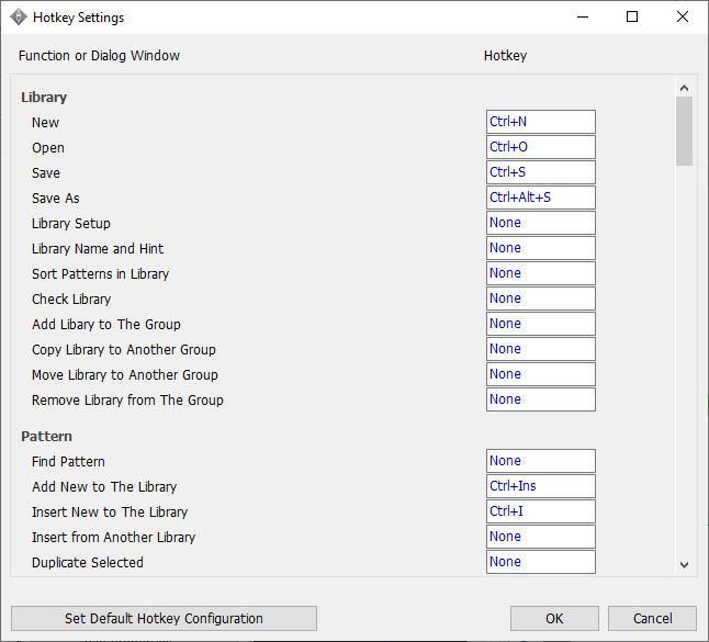
If the combination is already in use, a warning message pops up. Notice that certain shortcuts are reserved by the program and are not customizable. Press OK to apply changes. To restore default configuration press Set Default Hotkey Configuration.
Hotkeys reserved by the system:
Ctrl Shift Shift + mouse Enter Esc Left arrow Right arrow Up arrow Down arrow Shift + S Alt+any key |
– hold down to invert selection; – hold down to add objects to selection; – orthogonal moving of selected objects; – complete action; – cancel action; – move object left, pan left while routing/building; – move object right, pan right while routing/building; – move object up, pan up while routing/building; – move object down, pan down while routing/building; – enable disable auto-panning; – reserved by the system. |
5.1.9. Environment Variables
According to DipTrace License Policy, the software can be used by one license holder on several devices. To ensure smooth portability of your projects, DipTrace features an Environment Variables tool that allows setting variables for the paths to directories containing libraries, 3D models, images, etc. on different machines.
Go to Tools/ Environment Variables to open the Environment Variables dialog.
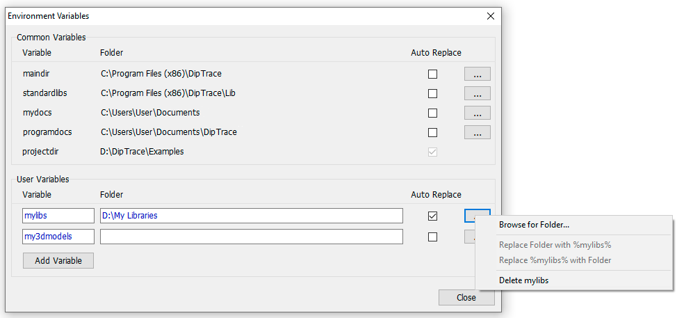
In the Common Variables section you can see the paths used by the software during installation and the corresponding variables for those paths.
In the User Variables part you can establish new variables for the paths to the directories, where your libraries or 3D models are stored. Type the variable in the Variable cell and set the path in the Folder line or press  button and select Browse for Folder to select the directory. Use the same variable on another PC to associate it with the path to the required folder on that machine. In this way when switching between machines the software will look for the files using the path corresponding to the established variable on the given PC.
You can check the Auto Replace option for the software to substitute the path with the variable in any items with such path as soon as they appear in the project or press button and select “Replace folder with %variable name%” to apply this command to all currently existing items in the project. To reverse the command select “Replace %variable name% with Folder” from the menu.
Remember to use the same variables to set the paths to the corresponding folders on another machine. If your component or 3D model libraries have been changed, make sure to update them in the source folder on your device.
To delete a variable press and select Delete <Variable Name>.
Environment Variables feature also allows creating a portable version of the program by establishing a variable for the launch directory, which can be stored, for instance, on a portable drive.
5.2. Working with libraries
5.2.1. General properties
In DipTrace a typical electronic component consists of a schematic symbol, a PCB footprint (pattern) and possibly a 3D model. All these entities represent a single component at various design stages. Pattern editor is the tool to create and edit component footprints and connect 3D models to patterns. In the Component Editor the designer connects a schematic symbol to a pattern to create a complete component, which is stored in the component libraries (files with *.eli extension).
DipTrace stores patterns separately from schematic symbols in the pattern libraries (files with *.lib extension on your computer).
Library has two basic string parameters: name and hint. Select "Library / Library Name and Hint" from the main menu to change them. Name is displayed on the Place Component panel in the PCB Layout and other software modules (10 characters max. recommended).
5.2.2. Library groups
Library groups are very easy means of organizing libraries. There are three default library groups: Patterns, User Patterns, and Other Libraries (auto-generated library group for storing pattern templates and separate library files).
Press  to change active library group or open the Library Setup dialog box to create and edit library groups and connect separate libraries from the files.
Press  to change move/copy/delete pattern libraries between the library groups.
5.2.3. Library setup
To manage the library groups, select "Library \ Library Setup" from the main menu or press and select Library Setup from the submenu.
It's possible to create as many library groups as needed and add/delete/libraries to the groups in the Library Setup dialog box regardless of their type and active DipTrace module. The Library Setup dialog box is the same in the PCB Layout and all other software modules.
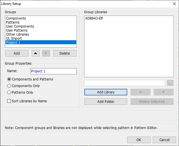
Press Add to add a new library group, type in the name into the field below and select the group type, depending on what libraries you are going to store in this group. Components Only allows for adding only component libraries (*.eli files) to the group, Patterns Only – only patterns (*.lib files), Components and Patterns – both.
To add a new library to the library group, press Add Library or Add Folder buttons and select the library directly from the file on your computer.
The user can not edit the standard library groups: Components and Patterns library groups.
5.2.4. Create
When you launch the Pattern Editor (no command prompt), the last edited library will open by default.
To create a new library, select "Library \ New" from the main menu or press the corresponding button on the Standard toolbar or on the Library Manager panel. Library group for the library should be defined. DipTrace offers User Patterns library group by default, but you can select another library group.
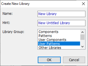
Go to Library Setup to create and manage library groups.
If current library is not saved and you try to create another library, the program will offer to save current library first. Notice that DipTrace does not allow you to modify standard libraries and library groups.
5.2.5. Open
To open a certain library, select it on the Library Manager panel. If the library is not in the list on the Library Manager panel, select "Library/ Open" from the main menu or press the corresponding button on the Standard toolbar and select a pattern library file (*.lib). The library will be automatically added to Other Libraries group. Use Library Setup dialog box to add this library to the required library groups.
5.2.6. Save
There are two items in the main menu to save a library: "Library/ Save" and "Library/ Save as". For the first option there is a corresponding tool on the Standard toolbar.
Select "Library/ Save" from the main menu or press the corresponding button on the Standard toolbar to save a library. If pattern library has never been saved, DipTrace will offer to create a new file for it. All user libraries are saved in the "Documents/ DipTrace/ My Libraries" folder by default. The program does not allow the user to modify standard libraries and library groups.
To save library into a different file, select "Library/ Save As" from the main menu.
5.2.7. Templates
It is much easier to create patterns using templates. When creating a new pattern, just select appropriate example pattern from the Template drop-down list on the Pattern Properties panel.
To edit the template library, select "Library \ Open Templates" from the main menu or select the Templates library in Other Libraries group on the Library Manager panel. You can add/edit/delete patterns to/from the Templates library like to a regular library with the same tools. To save certain library as a template, select "Library \ Save Templates" from the main menu.
5.2.8. Search patterns
To open Search Patterns dialog box, select "Pattern/ Find Pattern" from the main menu or "Pattern Tools/ Find Pattern" on the Library Manager panel.
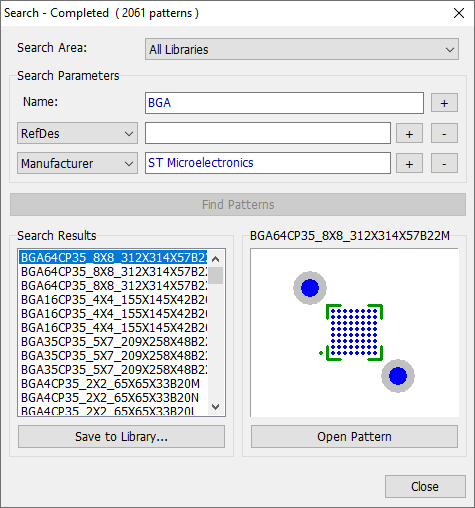
In the pop-up dialog box select a search area (active library, library group or all libraries). Specify name or part of the pattern's name as well as other pattern parameters. Press + button to add additional search filter parameters which allow the user to search patterns by manufacturer, datasheet, RefDes etc. (use the drop-down lists).
Click Find Patterns to start searching. Results will appear in the corresponding list. Preview selected pattern.
Press Save to Library in order to save the pattern to a new library. Press Open Pattern to open the library and the pattern for editing.
5.2.9. Search at SnapEDA
To look for the required components in SnapEDA libraries, go to "Pattern \ Search Parts at SnapEDA". In the pop-up, register or log-in, if necessary, then enter data in the Search field and press  button.
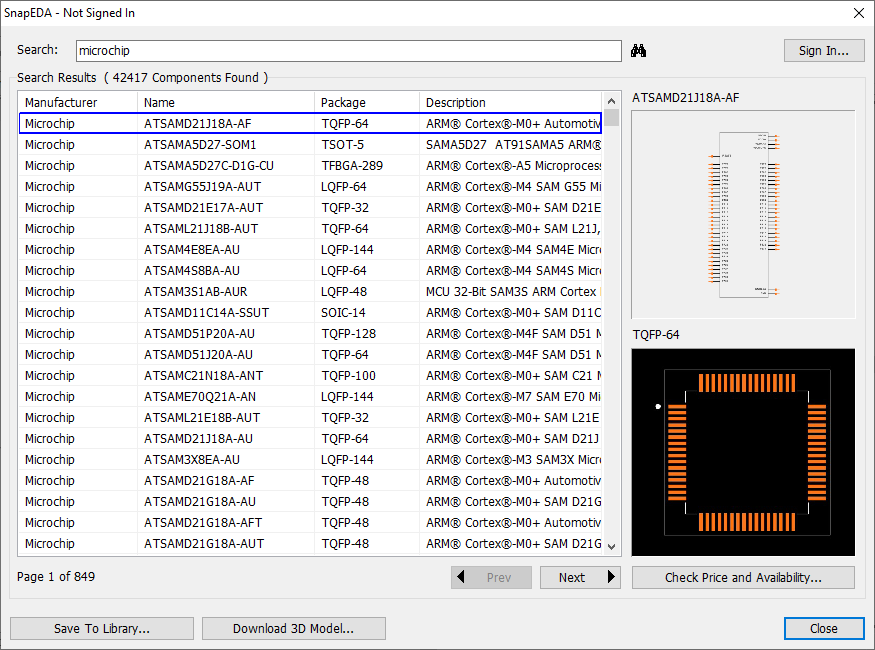
Select a component from the search results, its symbol and pattern will appear in the preview field, if available.
Press Save to Library button to add the component to the existing user library or to a newly-created one.
Download 3D Model button gets active, if a 3D model is available for the selected component. Press it to download the .step file to your computer. The model will be automatically attached to the respective pattern.
5.2.10. Working with patterns
The functions to work with the patterns of the current library can be accessed from the Pattern and Library menus as well as from Library Manager panel by pressing Pattern Tools and Library Tools buttons.
There are the following functions to work with patterns of the current library:
Find Pattern – open the Search Patterns dialog box to find required pattern in the libraries.
Add New Pattern to <current library> – add a new pattern to the library. This function can also be accessed via "Pattern/ Add New to <current library>" in the main menu.
Insert New Pattern to <current library> – insert new (blank) or existing pattern from another library into current position of an active library. This function can also be accessed via "Pattern/ Insert ..." from the main menu.
Insert Patterns from another library – get pattern from another pattern or component library into the current position of an active library. Select "Pattern/ Insert New from Another Library" from the main menu.
Duplicate patterns – select pattern in the list, press Pattern Tools, and choose Duplicate Patterns from the submenu. The copy of the pattern will appear right below the original one.
Move Patterns Up – move current pattern up in the library. Select "Pattern/ Move Up" from the main menu.
Move Patterns Down – move current pattern down in the library. Select "Pattern/ Move Down" from the main menu.
Move Patterns to the End – move current pattern to the end of the library.
Copy Patterns to Another Library – copy selected patterns to another library.
Move Patterns to Another Library – move selected patterns to another library.
Delete Patterns – delete selected patterns from the library. This function can also be accessed via "Pattern/ Delete from Library" from the main menu.
Sorting patterns in <current library> – automatically sort patterns by name in the selected library. Select "Library Tools/ Sort Patterns in <current library>" from the main menu.
Clear Pattern – delete all pads, shapes and mounting holes of the pattern. Select "Pattern/ Clear <current pattern>" from the main menu.
Inserting a group of patterns from another library – select position in the patterns list, right-click and choose Insert Patterns from Another Library. Select library and patterns you need in the pop-up dialog box (use Ctrl and Shift keys for multiple selection). Then press Insert to insert patterns into existing library.
Deleting a group of patterns from the library – select patterns in the patterns list (move mouse to the first pattern, hold down the left mouse button, move mouse pointer to the last pattern and release button) then press Pattern Tools or right-click on the patterns table and select Delete Pattern from the submenu.
5.2.11. Verification
Library Verification feature checks the number of patterns and pads in the library and displays possible errors: patterns with similar names (the library should be sorted), similar pad numbers and through pads without holes (this may happen if you think you've created an SMD pad, but set the hole size close to zero).
To display the library verification dialog box, select "Library/ Check <current library>" from the main menu.
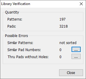
5.2.12. Import/Export
5.2.12.1. DipTrace ASCII import
DipTrace allows you to save/open data in the textual DipTrace ASCII format. This format has been developed to allow for data transferring from/to other EDA packages and for forward compatibility between the DipTrace versions.
To import DipTrace ASCII-formatted library file, select "Library/ Import/ DipTrace ASCII" then select file, and click OK.
5.2.12.2. DipTrace XML import
DipTrace Pattern Editor allows saving/ opening data in the textual DipTrace XML format. This format can be used for data transferring from/to other EDA packages and for forward compatibility between the DipTrace versions.
To import a library file in DipTrace XML format, select "Library/ Import/ DipXML" then select file, and click OK.
5.2.12.3. Altium ASCII import
DipTrace allows the user to import pattern libraries from Altium, using Altium ASCII format (*.lia).
Launch Altium, select PCB library, then go to "File/ Save copy as" from the main menu, select Export P-CAD V16 PCB Library (*.lia) File Type in the pop-up dialog box, and press Save. Now launch DipTrace Pattern Editor, select "Library/ Import/ P-CAD/Altium ASCII (*.lia)" from the main menu, select Altium PCB library, and press Open.
5.2.12.4. Eagle import
There are two ways to import pattern libraries from the EAGLE software: Eagle Script and EAGLE XML formats.
EAGLE XML Import (recommended)
Select "Library/ Import/ EAGLE XML" from the main menu in the Pattern Editor, and select an EAGLE library file (*.lbr) that you want to import.
EAGLE Script import
To create a script file, launch EAGLE software, select "Library/ Export/ Script" from the main menu. Save EAGLE library as an *.scr file. Now close the EAGLE software and open DipTrace Pattern Editor, select "Library/ Import/ Eagle Script (*.scr)" from the main menu and select that *.scr file.
5.2.12.5. EasyEDA Pro
DipTrace supports importing libraries from the EasyEDA Pro format (*.epro).
To import, choose "Library \ Import \ EasyEDA Pro" from the main menu in the DipTrace Pattern Editor, then select the desired EasyEDA Pro Project file (*.epro).
In the pop-up dialog, enter the Library Name and Hint, and select a Library Group for the imported library. Click OK to complete the import.
5.2.12.6. P-CAD import
DipTrace allows designers to import pattern libraries from P-CAD using P-CAD ASCII format (*.lia).
In order to create an ASCII library in P-CAD, open P-CAD Library Executive, select "Library/ Translate" from the main menu, select "From: P-CAD Binary", "To: P-CAD ASCII" in the pop-up dialog box, specify the library files, and press Translate.
Now close P-CAD Library Executive and open DipTrace Pattern Editor, select "Library/ Import/ P-CAD ASCII (*.lia)" from the main menu and open a *.lia file.
5.2.12.7. PADS import
DipTrace allows the user to import pattern libraries from PADS, using PADS ASCII format.
In PADS schematic symbols, pattern footprints and so called "logic" of a single component library are saved in separate files (*.p – parts, *.c – "logic" files, *.d – footprints), we recommend to start importing a component library by importing the footprint library in the Pattern Editor.
To import a footprint library from PADS, select "Library/ Import / PADS ASCII (*.p, *.d)" from the main menu in the Pattern Editor. Select a PADS library file (*.d) and press Open.
Some PADS footprint libraries (*.d - files) import with incorrect pad numbers (mostly BGA footprints). If you have imported a PADS footprint library with wrong pad numbers, select "Library \ Import \ PADS ASCII (*.p, *.d)" from the main menu in the Pattern Editor and import a respective *.p - file to fix pad numbers of the patterns.
5.2.12.8. DXF Import
DipTrace allows the designer to import a whole component pattern or its part from a DXF file.
To import DXF file, select "Pattern/ Import from DXF" from the main menu in the Pattern Editor, then select and open existing DXF file.
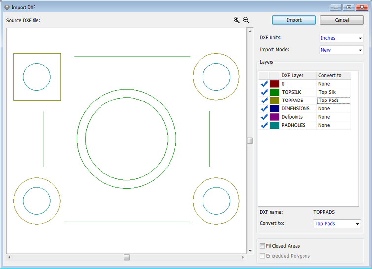
In the pop-up dialog box you can preview selected DXF file and specify connections between the DXF and DipTrace PCB layers. To set connection between DXF and PCB layers, select layer from the DXF layers list, and a corresponding DipTrace layer in the Convert to drop-down list.
To show/hide different layers of the DXF file, click on the first column of the Layers table (blue check marks).
Notice that import feature has recognition options, i.e., for example, if you have pad shapes in one DXF layer and all drills (including the mounting holes) in another layer, then specify "Pads" for the first layer and "All Holes" for the second layer. You will get through-hole pads with holes inside pad shapes, surface pads without holes and mounting holes (without shapes).
DipTrace can Fill Closed Areas and recognize polygons embedded, check respective check boxes in the Import DXF dialog box.
5.2.12.9. KiCAD import
DipTrace allows the user to import pattern libraries from KiCAD.
In DipTrace Pattern Editor, select "Library / Import / KiCAD Dir" from the main menu, select KiCAD library folder.
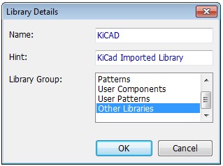
In the pop-up window type-in the Library name, hint and choose a Library Groop (User Pattern or Other libraries). Press OK.
Some KiCAD libraries may have patterns with repeated pad numbers. DipTrace does not allow repetition in pad numbering, therefore, a warning message will appear when importing a library containing such footprints.
To be able to use patterns imported with incorrect pad numbering, launch Library check (Library/ Check <current library> in the Main Menu) to find such patterns and renumber their pads.
5.2.12.10. DipTrace ASCII export
DipTrace Pattern Editor allows the user to save/open data in the textual ASCII format. This format has been developed to allow data transfer from/to other EDA packages and for forward compatibility.
To export a library file to DipTrace ASCII format, select "Library \ Export \ DipTrace ASCII", then define the filename, and click OK.
5.2.12.11. DipTrace XML export
DipTrace Pattern Editor allows saving/ opening data in the textual DipTrace XML format. This format can be used for data transferring from/to other EDA packages and for forward compatibility between the DipTrace versions.
To export a library file in DipTrace XML format, select "Library/ Export/ DipXML" then define filename, and click OK.
5.2.12.12. Eagle XML export
DipTrace Pattern Editor allows the user to save library in Eagle XML format to enable data transfer to Eagle for forward compatibility with this EDA tool.
To export library file in Eagle XML format, select "Library \ Export \ Eagle XML (*.lbr)", then define the filename, and click OK.
5.3. Designing a pattern
5.3.1. Review, properties
Component pattern (footprint) consists of pads, shapes and can also include mounting holes and fiducials. Patterns are united into pattern libraries (files with *.lib extension).
Pattern has the following properties: name (including unique name and name description), RefDes, value, manufacturer and several user-defined fields. All properties can be changed on the Pattern Properties panel.
DipTrace has 11 different styles of patterns (8 types are selected from the drop-down list on Pattern Properties panel in the Pattern Editor and 3 pattern modes in the PCB Layout):
1. Free – does not depend on pattern parameters. All pads can be placed anywhere.
2. IPC-7351 – launches Pattern Generator that allows creating footprints and 3D models to IPC standards.
3. Circle – pads form a circle. This mode depends on number of pads and pad-to-pad spacing.
4. Lines – pads form lines. This mode depends on four parameters: number of lines, number of pads, pad-to-pad spacing and line-to-line spacing.
5. Square – four lines of pads which form a square. This mode depends on three parameters: number of pads, pad-to-pad spacing and line-to-line spacing.
6. Matrix – pattern's pads form a matrix. This mode depends on the number of columns, number of rows, column spacing and row spacing.
7. Rectangle – four pad lines form a rectangle. This mode depends on 5 parameters: horizontal pads, vertical pads, pad spacing, width and height.
8. Zig-Zag – pads form a zig-zag. This mode depends on 3 parameters: number of pads, pad-to-pad spacing and line-to-line spacing.
9. Fiducial - a pattern comprises only one fiducial. It is created directly in the PCB Layout using Place Fiducial tool.
10. Pad – one-pad patterns. These are created directly in the PCB Layout with the Place Pad tool.
11. Mounting Hole – a pattern has only one mounting hole. It is created directly in the PCB Layout using Place Mounting Hole tool.
Pads can be through-hole or surface (SMD). For through-hole pads you can define hole dimensions, hole shape and X/Y offset of the pad shape from the hole center. Surface pads can be located on Top or Bottom side (inverted when pattern is placed to the bottom side of the board). Ellipse, obround, rectangle, D-shape and polygon shapes are available for pads. You can define width and height for all pads, for rectangle pads you can additionally set corner radius to get rounded corners, and for polygonal pads - set key points (it is possible to create regular or free polygons).
Right-click on a pad, and select Properties from the submenu to change pad properties for selected pad/s. If you want to change all pattern pads (default settings), use Standard Pad Properties dialog box ("Pattern \ Standard Pad Properties" from the main menu) or press Standard Pad Properties button on the Pattern Properties panel.
There are 9 shape types for drawing: line, arc, rectangle, filled rectangle, obround, filled obround, polyline, polygon and text object. Such shapes as line, polyline and polygon are defined by key points; arcs - by key points and curve radius; (filled) rectangle and (filled) obround shapes - by key points, width and height parameters. To change shape's properties, right-click on a shape, and select Properties from the submenu.
If you resize a pattern by changing numerical or spacing parameters, shape size is changed automatically. Shape can be located on any board layer. With a drop-down list on the Drawing toolbar you can predefine a layer for new shapes to be placed to. You can also change layer of the shapes that are already placed on the design area – go to Shape Properties dialog box (right-click on the shape, and select Properties from the submenu).
A mounting hole is defined by two parameters: hole and keepout area diameters. To set the parameters of a mounting hole, use the Placement Setup dialog box in the Pattern Editor.
A fiducial is defined by two parameters: copper and keepout area diameters. To set the parameters of a fiducial, use Fiducial Properties dialog accessed via right-click submenu.
5.3.2. Pattern Generator
5.3.2.1. Review
Pattern Generator helps create footprints with 3D models based on the key package parameters. IPC-7351 Standard is used for generation.
To launch Pattern Editor select IPC-7351 Style on Pattern Properties panel; IPC-7351 Pattern Generator button will appear right below. Press it to open Pattern Generator.
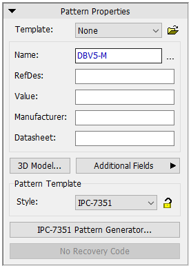
In the Pattern Generator dialog, select whether you want to create a package for a Surface Mount or Through Hole device and specify Family.
Press Show Details button to see more information about each Family.
Select Density Level – this setting is common for all tabs (Component Options, Terminal Options, Design Rules) in Surface Mount Families. You can create footprints of different sizes that can be used for various soldering types. This setting, depending on the Family, may define Pad Sizes, Silk, Courtyard and Fiduсials.
Set the units (mm/ inch/ mil) at the bottom of the dialog window.
The content of the tabs for defining package parameters change depending upon the selected family (see description for the most frequently-used families here: BGA; Chip; SOP, SOIC; QFP; SOT23; SON; QFN; Axial; DIP). Enter all the required values to create a footprint with a 3D model. Set Pattern Name, Pattern Properties.
Press Recalculate button and then OK.
5.3.2.2. Generating Surface Mount Package
5.3.2.2.1. BGA
5.3.2.2.1.1. Drawing Data
To Generate a BGA package, select Surface Mount device type, BGA family.
Check the images to find the required parameters in the datasheet.
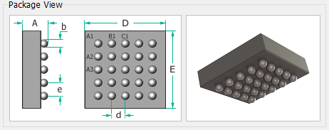
Fill in the red cells in the Drawing Data tab. DipTrace inserts calculated values in the non-required grey cells. Note that Required values can also be calculated based on the values in the non-required grey cells of the same line.
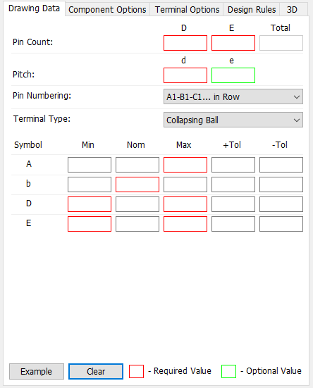
Select pin numbering pattern (by Row or by Column) and terminal type (Collapsing Ball/ Non-Collapsing Ball).
Press Example button to see sample values.
Press Clear button to clear all cells.
5.3.2.2.1.2. Component Options
In Component Options tab you can adjust a number of parameters.
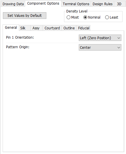
General:
| - | Pin 1 Orientation (Left, Up, Right, Down) |
| - | Pattern Origin (Center, Pin 1) |
Silk:
| - | With Include Silk option activated the software will create Silk Screen shapes for the pattern. Select Package dimensions to be used (min., nom., max.) and set the line width. |
| - | You can also choose to include Pin 1 Marker Dot. It’s size is set by Terminal Width value. |
Assembly:
| - | You can choose to include or not the Assembly layer. If included, you can select Package Dimensions (maximum, nominal, minimum) and set the Line Width. |
| - | Add or remove Polarity Marker. |
Courtyard:
| - | You can choose to include or not the Courtyard layer. If included, you can set the Line Width for the Courtyard shape; Shape Dimensions are set based on Courtyard to Maximum Package size value from the Design Rules. |
| - | Add or remove Origin Cross for the shapes in the Courtyard layer. |
| - | Add or remove Origin Target for the shapes in the Courtyard layer. |
Outline:
| - | You can choose to include or not the Component Outline. If included, you can set the Line Width for the Outline shape; the shape will be drawn by Nominal Values from Drawing Data. |
Fiducial:
| - | You can choose to include or not a Fiducial. If included, you can set the maximum pitch size, for which fiducial is added, as well as pad, solder mask and keepout diameters. |
Note that DipTrace remembers the parameters set for the previous package of the same family. You can enter new values or press Set Values by Default button to reset defaults for the given tab.
5.3.2.2.1.3. Terminal Options
In the Terminal Options section you can define the following parameters of the pads: custom solder mask swell, custom paste mask shrink, the way to display pads in assembly layer (don’t show/ contour/ filled shape); you can choose to include or not the Terminal Outline.
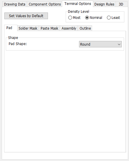
Note that DipTrace remembers the parameters set for the previous package of the same family. You can enter new values or press Set Values by Default button to reset defaults for the given tab.
5.3.2.2.1.4. Design Rules
Clearance values for the footprint elements (pad to pad, silk to pad) are set in the Design Rules tab.
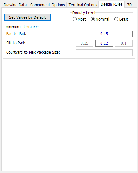
Note that DipTrace remembers the parameters set for the previous package of the same family. You can enter new values or press Set Values by Default button to reset defaults for the given tab.
5.3.2.2.1.5. 3D Model
In 3D tab you can adjust parameters for 3D model generation.
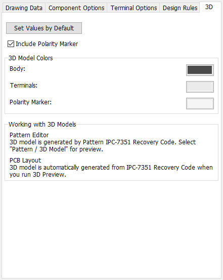
In Pattern Generator, footprints are created with 3D models. Those models are generated based on IPC-7351 Recovery Code in 3D preview mode both in Pattern Generator and PCB Layout modules.
5.3.2.2.2. Chip
5.3.2.2.2.1. Drawing Data
To Generate a Chip package, select Surface Mount device type, Chip family.
Check the images to find the required parameters in the datasheet.
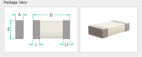
Select device SubFamily (Antenna, (Polarized/ Non-Polarized) Capacitor, (Polarized/ Non-Polarized) Diode, Ferrite Bead, Filter, Fuse, Non-Polarized Inductor, LED, Resistor, Thermistor, Varistor).
Fill in the red cells in the Drawing Data tab. DipTrace inserts calculated values in the non-required grey cells. Note that Required values can also be calculated based on the values in the non-required grey cells of the same line.
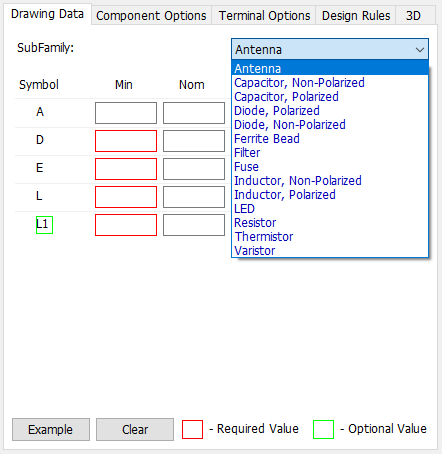
Press Example button to see sample values.
Press Clear button to clear all cells.
5.3.2.2.2.2. Component Options
In Component Options tab you can adjust a number of parameters.
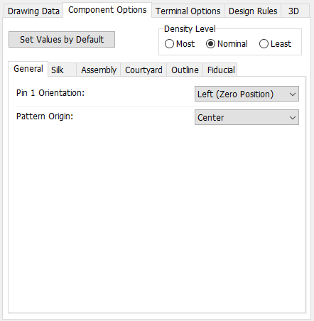
General:
| - | Pin 1 Orientation (Left, Up, Right, Down) |
| - | Pattern Origin (Center, Pin 1) |
Silk:
| - | With Include Silk option activated the software will create Silk Screen shapes for the pattern. Select Package dimensions to be used (min., nom., max.) and set the line width. |
| - | You can also choose to include Pin 1 Marker Line and/ or Dot with defined diameter for polarized subfamilies. |
Assembly:
| - | You can choose to include or not the Assembly layer. If included, you can select Package Dimensions (maximum, nominal, minimum) and set the Line Width. |
| - | Add or remove Polarity Marker. |
Courtyard:
| - | You can choose to include or not the Courtyard layer. If included, you can set the Line Width for the Courtyard shape; Shape Dimensions are set based on Courtyard to Maximum Package size/ to Pad value from the Design Rules. |
| - | Add or remove Origin Cross for the shapes in the Courtyard layer. |
| - | Add or remove Origin Target for the shapes in the Courtyard layer. |
Outline:
| - | You can choose to include or not the Outline. If included, you can set the Line Width for the Outline shape; the shape will be drawn by Nominal Values from the Drawing Data. |
Fiducial:
| - | Placing fiducial is not applicable for this Family. |
DipTrace remembers the parameters set for the previous package of the same family. You can enter new values or press Set Values by Default button to reset defaults for the given tab.
5.3.2.2.2.3. Terminal Options
In the Terminal Options section you can define all the parameters of the pads: their shape (rounded rectangle, rectangle), pad corner radius for Rounded Rectangle pad shape, cathode and anode numbering for polarized components, custom solder mask swell, custom paste mask shrink, the way to display pads in assembly layer (don’t show/ contour/ filled shape); you can also choose to include or not the Terminal Outline.
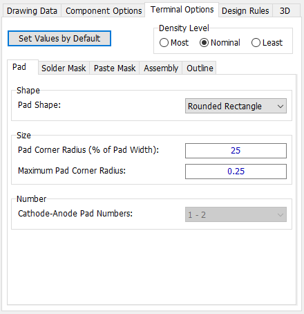
DipTrace remembers the parameters set for the previous package of the same family. You can enter new values or press Set Values by Default button to reset defaults for the given tab.
5.3.2.2.2.4. Design Rules
Clearance values for the footprint elements (pad to pad, silk to pad) are set in the Design Rules tab.
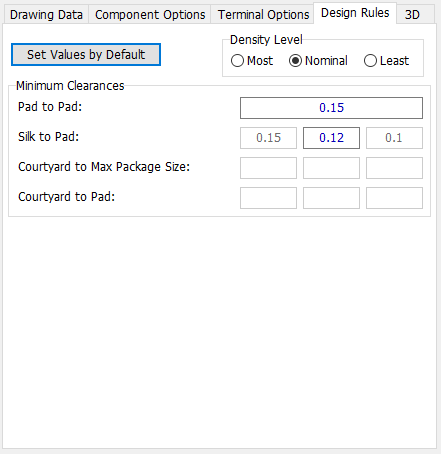
DipTrace remembers the parameters set for the previous package of the same family. You can enter new values or press Set Values by Default button to reset defaults for the given tab.
5.3.2.2.2.5. 3D Model
In 3D tab you can adjust parameters for 3D model generation.
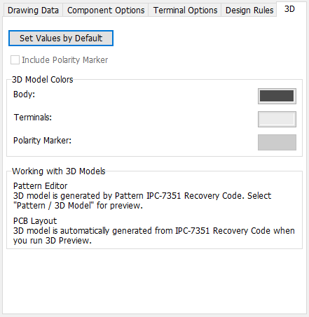
In Pattern Generator, footprints are created with 3D models. Those models are generated based on IPC-7351 Recovery Code in 3D preview mode both in Pattern Generator and PCB Layout modules.
5.3.2.2.3. QFN with Tab
5.3.2.2.3.1. Drawing Data
To Generate a QFN with Tab package, select Surface Mount device type, “QFN with Tab” family.
Check the images to find the required parameters in the datasheet.
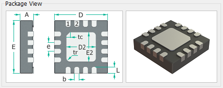
Select Lead shape from the drop-down (rectangle, D-shape).
Fill in the red cells in the Drawing Data tab. DipTrace inserts calculated values in the non-required grey cells. Note that Required values can also be calculated based on the values in the non-required grey cells of the same line.
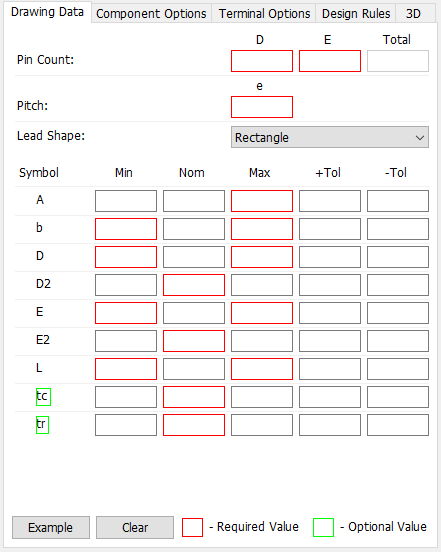
Press Example button to see sample values.
Press Clear button to clear all cells.
5.3.2.2.3.2. Component Options
In Component Options tab you can adjust a number of parameters.
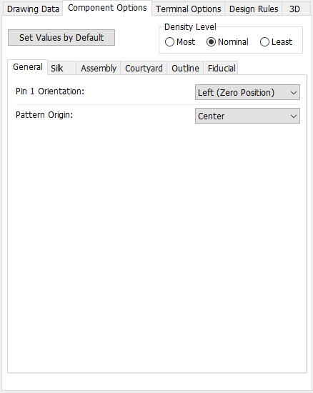
General:
| - | Pin 1 Orientation (Left, Up, Right, Down). |
| - | Pattern Origin (Center, Pin 1). |
Silk:
| - | With Include Silk option activated the software will create Silk Screen shapes for the pattern. Select Package dimensions to be used (min., nom., max.) and set the line width. |
| - | You can also choose to include Pin 1 Marker Line and/ or Dot. |
Assembly:
| - | You can choose to include or not the Assembly layer. If included, you can select Package Dimensions (maximum, nominal, minimum) and set the Line Width. |
| - | Add or remove Polarity Marker. |
Courtyard:
| - | You can choose to include or not the Courtyard layer. If included, you can set the Line Width for the Courtyard shape; Shape Dimensions are set based on Courtyard to Maximum Package size/ to Pad value from the Design Rules. |
| - | Add or remove Origin Cross for the shapes in the Courtyard layer. |
| - | Add or remove Origin Target for the shapes in the Courtyard layer. |
Outline:
| - | You can choose to include or not the Component Outline. If included, you can set the Line Width for the Outline shape; the shape will be drawn by Nominal Values from the Drawing Data. |
Fiducial:
| - | Placing fiducial is not applicable for this Family. |
DipTrace remembers the parameters set for the previous package of the same family. You can enter new values or press Set Values by Default button to reset defaults for the given tab.
5.3.2.2.3.3. Terminal Options
In the Terminal Options section you can define all the parameters of the pads: their shape (D-shape, obround, rounded rectangle, rectangle), the shape of the first pad (obround, rounded rectangle, rectangle), pad corner radius for Rounded Rectangle pad shape, custom solder mask swell, custom paste mask shrink, the way to display pads in assembly layer (don’t show/ contour/ filled shape); you can also choose to include or not the Terminal Outline.
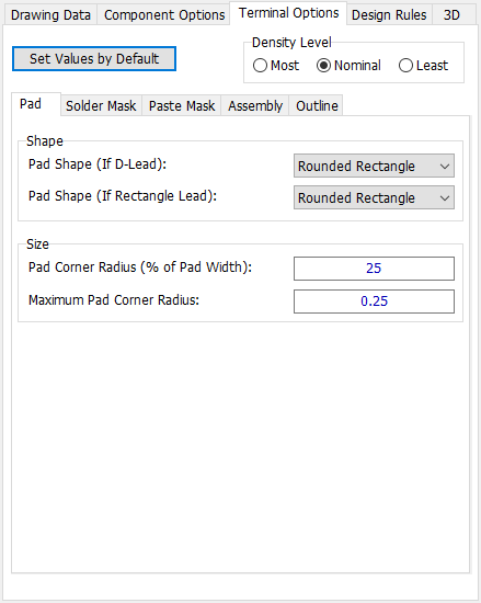
DipTrace remembers the parameters set for the previous package of the same family. You can enter new values or press Set Values by Default button to reset defaults for the given tab.
5.3.2.2.3.4. Design Rules
Clearance values for the footprint elements (pad to pad, pad to thermal tab, silk to pad) are set in the Design Rules tab.
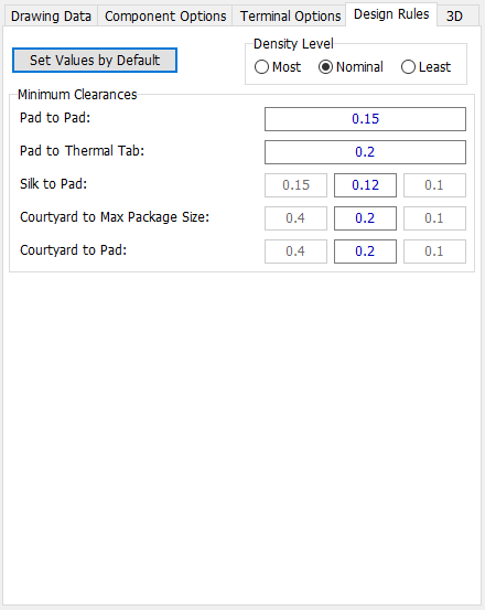
DipTrace remembers the parameters set for the previous package of the same family. You can enter new values or press Set Values by Default button to reset defaults for the given tab.
5.3.2.2.3.5. 3D Model
In 3D tab you can adjust parameters for 3D model generation.
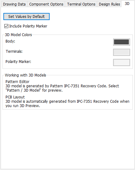
In Pattern Generator, footprints are created with 3D models. Those models are generated based on IPC-7351 Recovery Code in 3D preview mode both in Pattern Generator and PCB Layout modules.
5.3.2.2.4. QFP
5.3.2.2.4.1. Drawing Data
To Generate a QFP package, select Surface Mount device type, QFP family.
Check the images to find the required parameters in the datasheet.
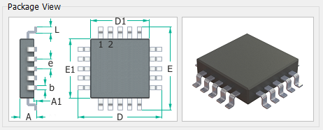
Fill in the red cells in the Drawing Data tab. DipTrace inserts calculated values in the non-required grey cells. Note that Required values can also be calculated based on the values in the non-required grey cells of the same line.
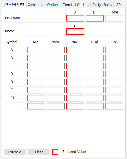
Press Example button to see sample values.
Press Clear button to clear all cells.
5.3.2.2.4.2. Component Options
In Component Options tab you can adjust a number of parameters.
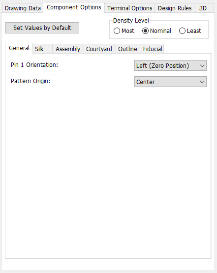
General:
| - | Pin 1 Orientation (Left, Up, Right, Down) |
| - | Pattern Origin (Center, Pin 1) |
Silk:
| - | With Include Silk option activated the software will create Silk Screen shapes for the pattern. Select Package dimensions to be used (min., nom., max.) and set the line width. |
| - | You can also choose to include Pin 1 Marker Line and/ or Dot with defined diameter. |
Assembly:
| - | You can choose to include or not the Assembly layer. If included, you can select Package Dimensions (maximum, nominal, minimum) and set the Line Width. |
| - | Add or remove Polarity Marker. |
Courtyard:
| - | You can choose to include or not the Courtyard layer. If included, you can set the Line Width for the Courtyard shape; Shape Dimensions are set based on Courtyard to Maximum Package size value from the Design Rules. |
| - | Add or remove Origin Cross for the shapes in the Courtyard layer. |
| - | Add or remove Origin Target for the shapes in the Courtyard layer. |
Outline:
| - | You can choose to include or not the Component Outline. If included, you can set the Line Width for the Outline shape; the shape will be drawn by Nominal Values from Drawing Data. |
Fiducial:
| - | You can choose to include or not a Fiducial. If included, you can set the maximum pitch size, for which fiducial is added, as well as pad, solder mask and keepout diameters. |
Note that DipTrace remembers the parameters set for the previous package of the same family. You can enter new values or press Set Values by Default button to reset defaults for the given tab.
5.3.2.2.4.3. Terminal Options
In the Terminal Options section you can define all the parameters of the pads: their shape, custom solder mask swell, custom paste mask shrink, the way to display pads in assembly layer (don’t show/ contour/ filled shape); you can choose to include or not the Terminal Outline.
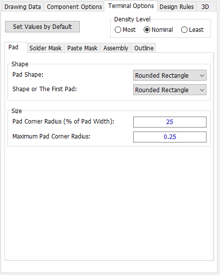
Note that DipTrace remembers the parameters set for the previous package of the same family. You can enter new values or press Set Values by Default button to reset defaults for the given tab.
5.3.2.2.4.4. Design Rules
Clearance values for the footprint elements (pad to pad, silk to pad) are set in the Design Rules tab.
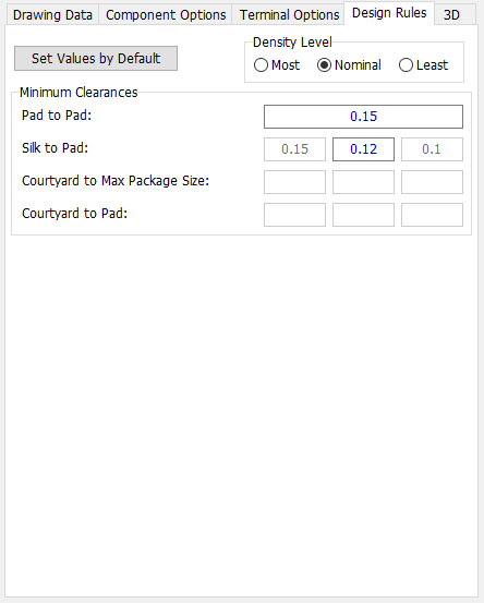
Note that DipTrace remembers the parameters set for the previous package of the same family. You can enter new values or press Set Values by Default button to reset defaults for the given tab.
5.3.2.2.4.5. 3D Model
In 3D tab you can adjust parameters for 3D model generation.
In Pattern Generator, footprints are created with 3D models. Those models are generated based on IPC-7351 Recovery Code in 3D preview mode both in Pattern Generator and PCB Layout modules.
5.3.2.2.5. SON with Tab
5.3.2.2.5.1. Drawing Data
To Generate a SON with Tab package, select Surface Mount device type, “SON with Tab” family.
Check the images to find the required parameters in the datasheet.
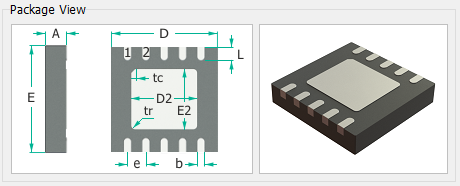
Select Lead shape from the drop-down (rectangle, D-shape).
Fill in the red cells in the Drawing Data tab. DipTrace inserts calculated values in the non-required grey cells. Note that Required values can also be calculated based on the values in the non-required grey cells of the same line.
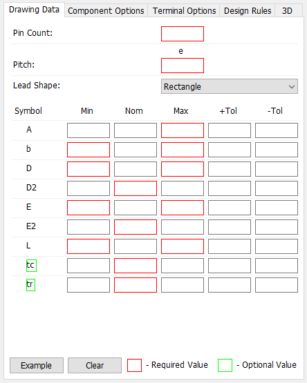
Press Example button to see sample values.
Press Clear button to clear all cells.
5.3.2.2.5.2. Component Options
In Component Options tab you can adjust a number of parameters.
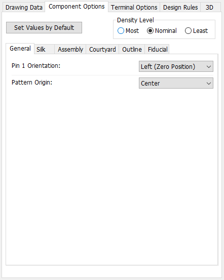
General:
| - | Pin 1 Orientation (Left, Up, Right, Down) |
| - | Pattern Origin (Center, Pin 1) |
Silk:
| - | With Include Silk option activated the software will create Silk Screen shapes for the pattern. Select Package dimensions to be used (min., nom., max.) and set the line width. |
| - | You can also choose to include Pin 1 Marker Line and/ or Dot. |
Assembly:
| - | You can choose to include or not the Assembly layer. If included, you can select Package Dimensions (maximum, nominal, minimum) and set the Line Width. |
| - | Add or remove Polarity Marker. |
Courtyard:
| - | You can choose to include or not the Courtyard layer. If included, you can set the Line Width for the Courtyard shape; Shape Dimensions are set based on Courtyard to Maximum Package size/ to Pad value from the Design Rules. |
| - | Add or remove Origin Cross for the shapes in the Courtyard layer. |
| - | Add or remove Origin Target for the shapes in the Courtyard layer. |
Outline:
| - | You can choose to include or not the Component Outline. If included, you can set the Line Width for the Outline shape; the shape will be drawn by Nominal Values from the Drawing Data. |
Fiducial:
| - | Placing fiducial is not applicable for this Family. |
DipTrace remembers the parameters set for the previous package of the same family. You can enter new values or press Set Values by Default button to reset defaults for the given tab.
5.3.2.2.5.3. Terminal Options
In the Terminal Options section you can define all the parameters of the pads: their shape (D-shape, obround, rounded rectangle, rectangle), the shape of the first pad (obround, rounded rectangle, rectangle), pad corner radius for Rounded Rectangle pad shape, custom solder mask swell, custom paste mask shrink, the way to display pads in assembly layer (don’t show/ contour/ filled shape); you can also choose to include or not the Terminal Outline.
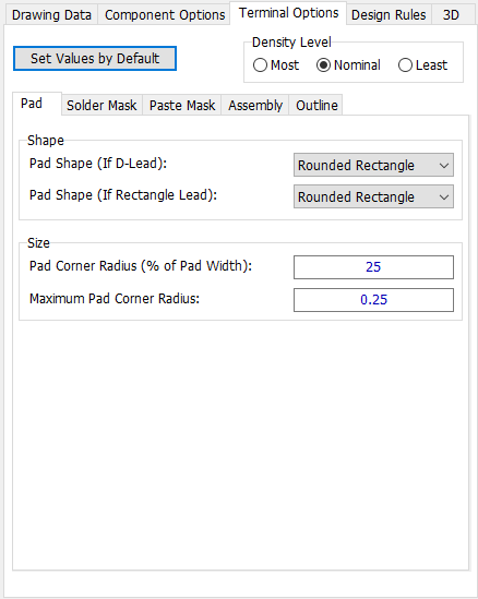
DipTrace remembers the parameters set for the previous package of the same family. You can enter new values or press Set Values by Default button to reset defaults for the given tab.
5.3.2.2.5.4. Design Rules
Clearance values for the footprint elements (pad to pad, pad to thermal tab, silk to pad) are set in the Design Rules tab.
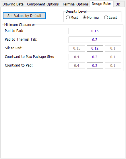
DipTrace remembers the parameters set for the previous package of the same family. You can enter new values or press Set Values by Default button to reset defaults for the given tab.
5.3.2.2.5.5. 3D Model
In 3D tab you can adjust parameters for 3D model generation.
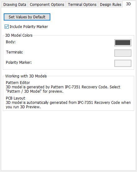
In Pattern Generator, footprints are created with 3D models. Those models are generated based on IPC-7351 Recovery Code in 3D preview mode both in Pattern Generator and PCB Layout modules.
5.3.2.2.6. SOP, SOIC
5.3.2.2.6.1. Drawing Data
To Generate a SOP, SOIC package, select Surface Mount device type, “SOP, SOIC” family.
Check the images to find the required parameters in the datasheet.
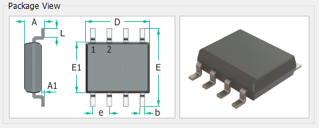
Fill in the red cells in the Drawing Data tab. DipTrace inserts calculated values in the non-required grey cells. Note that Required values can also be calculated based on the values in the non-required grey cells of the same line.
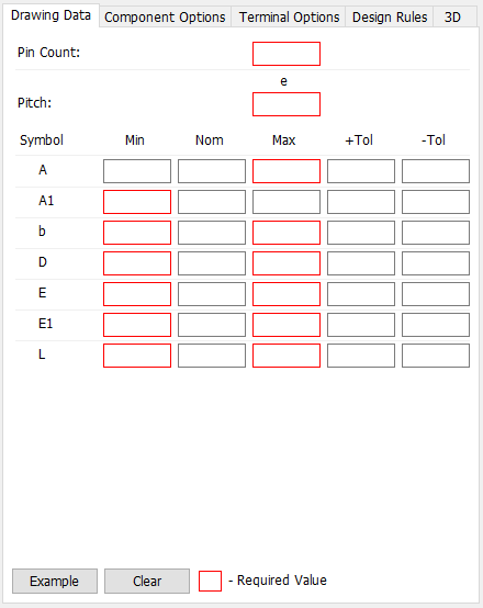
Press Example button to see sample values.
Press Clear button to clear all cells.
5.3.2.2.6.2. Component Options
In Component Options tab you can adjust a number of parameters.
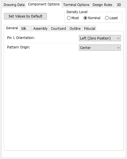
General:
| - | Pin 1 Orientation (Left, Up, Right, Down) |
| - | Pattern Origin (Center, Pin 1) |
Silk:
| - | With Include Silk option activated the software will create Silk Screen shapes for the pattern. Select Package dimensions to be used (min., nom., max.) and set the line width. |
| - | You can also choose to include Pin 1 Marker Line and/ or Dot with defined diameter. |
Assembly:
| - | You can choose to include or not the Assembly layer. If included, you can select Package Dimensions (maximum, nominal, minimum) and set the Line Width. |
| - | Add or remove Polarity Marker. |
Courtyard:
| - | You can choose to include or not the Courtyard layer. If included, you can set the Line Width for the Courtyard shape; Shape Dimensions are set based on Courtyard to Maximum Package size/ to Pad value from the Design Rules. |
| - | Add or remove Origin Cross for the shapes in the Courtyard layer. |
| - | Add or remove Origin Target for the shapes in the Courtyard layer. |
Outline:
| - | You can choose to include or not the Component Outline. If included, you can set the Line Width for the Outline shape; the shape will be drawn by Nominal Values from the Drawing Data. |
Fiducial:
| - | Placing fiducial is not applicable for this Family. |
DipTrace remembers the parameters set for the previous package of the same family. You can enter new values or press Set Values by Default button to reset defaults for the given tab.
5.3.2.2.6.3. Terminal Options
In the Terminal Options section you can define all the parameters of the pads: their shape (rounded rectangle, rectangle, obround), the shape of the first pad (rounded rectangle, rectangle, obround), pad corner radius for Rounded Rectangle pad shape, custom solder mask swell, custom paste mask shrink, the way to display pads in assembly layer (don’t show/ contour/ filled shape); you can also choose to include or not the Terminal Outline.
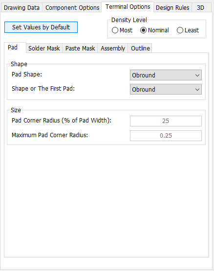
DipTrace remembers the parameters set for the previous package of the same family. You can enter new values or press Set Values by Default button to reset defaults for the given tab.
5.3.2.2.6.4. Design Rules
Clearance values for the footprint elements (pad to pad, silk to pad) are set in the Design Rules tab.
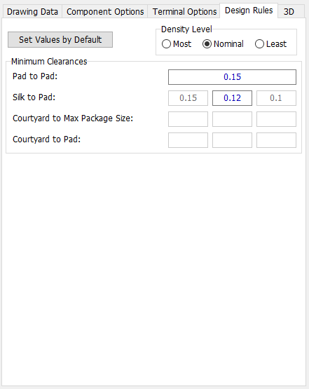
DipTrace remembers the parameters set for the previous package of the same family. You can enter new values or press Set Values by Default button to reset defaults for the given tab.
5.3.2.2.6.5. 3D Model
In 3D tab you can adjust parameters for 3D model generation.
In Pattern Generator, footprints are created with 3D models. Those models are generated based on IPC-7351 Recovery Code in 3D preview mode both in Pattern Generator and PCB Layout modules.
5.3.2.2.7. SOT23
5.3.2.2.7.1. Drawing Data
To Generate a SOT 23 package, select Surface Mount device type, SOT 23 family.
Check the images to find the required parameters in the datasheet.
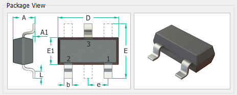
Fill in the red cells in the Drawing Data tab. DipTrace inserts calculated values in the non-required grey cells. Note that Required values can also be calculated based on the values in the non-required grey cells of the same line.
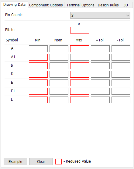
Press Example button to see sample values.
Press Clear button to clear all cells.
5.3.2.2.7.2. Component Options
In Component Options tab you can adjust a number of parameters.
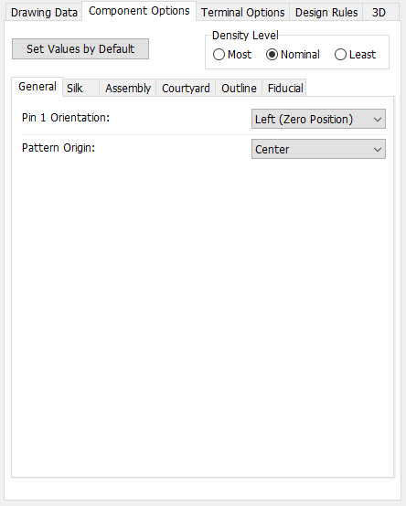
General:
| - | Pin 1 Orientation (Left, Up, Right, Down) |
| - | Pattern Origin (Center, Pin 1) |
Silk:
| - | With Include Silk option activated the software will create Silk Screen shapes for the pattern. Select Package dimensions to be used (min., nom., max.) and set the line width. |
| - | You can also choose to include Pin 1 Marker Line and/ or Dot with defined diameter. |
Assembly:
| - | You can choose to include or not the Assembly layer. If included, you can select Package Dimensions (maximum, nominal, minimum) and set the Line Width. |
| - | Add or remove Polarity Marker. |
Courtyard:
| - | You can choose to include or not the Courtyard layer. If included, you can set the Line Width for the Courtyard shape; Shape Dimensions are set based on Courtyard to Maximum Package size/ to Pad value from the Design Rules. |
| - | Add or remove Origin Cross for the shapes in the Courtyard layer. |
| - | Add or remove Origin Target for the shapes in the Courtyard layer. |
Outline:
| - | You can choose to include or not the Component Outline. If included, you can set the Line Width for the Outline shape; the shape will be drawn by Nominal Values from the Drawing Data. |
Fiducial:
| - | Placing fiducial is not applicable for this Family. |
DipTrace remembers the parameters set for the previous package of the same family. You can enter new values or press Set Values by Default button to reset defaults for the given tab.
5.3.2.2.7.3. Terminal Options
In the Terminal Options section you can define all the parameters of the pads: their shape (rounded rectangle, rectangle, obround), the shape of the first pad (rounded rectangle, rectangle, obround), pad corner radius for Rounded Rectangle pad shape, custom solder mask swell, custom paste mask shrink, the way to display pads in assembly layer (don’t show/ contour/ filled shape); you can also choose to include or not the Terminal Outline.
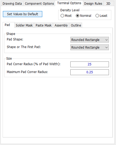
DipTrace remembers the parameters set for the previous package of the same family. You can enter new values or press Set Values by Default button to reset defaults for the given tab.
5.3.2.2.7.4. Design Rules
Clearance values for the footprint elements (pad to pad, silk to pad) are set in the Design Rules tab.
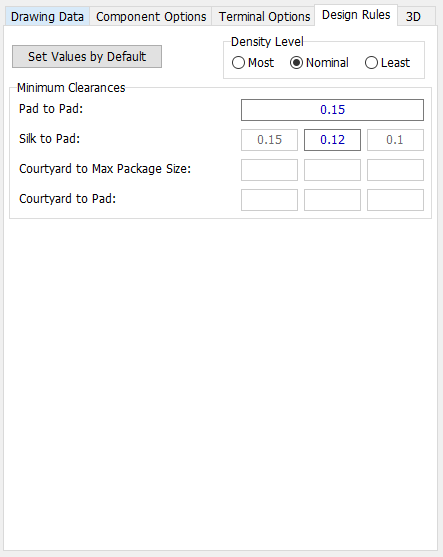
DipTrace remembers the parameters set for the previous package of the same family. You can enter new values or press Set Values by Default button to reset defaults for the given tab.
5.3.2.2.7.5. 3D Model
In 3D tab you can adjust parameters for 3D model generation.
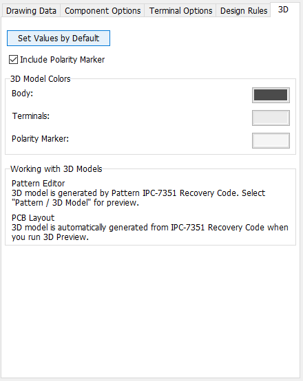
In Pattern Generator, footprints are created with 3D models. Those models are generated based on IPC-7351 Recovery Code in 3D preview mode both in Pattern Generator and PCB Layout modules.
5.3.2.3. Generating Through Hole Package
Enter topic text here.
5.3.2.3.1. Axial
5.3.2.3.1.1. Drawing Data
To Generate an Axial package, select Through Hole device type, Axial family.
Check the images to find the required parameters in the datasheet.
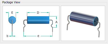
Select SubFamily from the drop-down (polarized/non-polarized capacitor, polarized/non-polarized diode, fuse,non-polarized inductor, resistor).
Fill in the red cells in the Drawing Data tab. DipTrace inserts calculated values in the non-required grey cells. Note that Required values can also be calculated based on the values in the non-required grey cells of the same line.
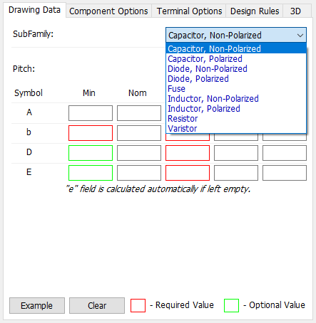
Press Example button to see sample values.
Press Clear button to clear all cells.
5.3.2.3.1.2. Component Options
In Component Options tab you can adjust a number of parameters.
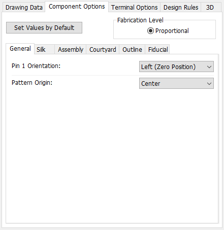
General:
| - | Pin 1 Orientation (Left, Up, Right, Down). |
| - | Pattern Origin (Center, Pin 1). |
Silk:
| - | With Include Silk option activated the software will create Silk Screen shapes for the pattern. Select Package dimensions to be used (min., nom., max.) and set the line width. |
| - | You can also choose to include Pin 1 Marker Line and/ or Dot for polarized subfamilies. |
Assembly:
| - | You can choose to include or not the Assembly layer. If included, you can select Package Dimensions (maximum, nominal, minimum) and set the Line Width. |
| - | Add or remove Polarity Marker for polarized components. |
Courtyard:
| - | You can choose to include or not the Courtyard layer. If included, you can set the Line Width for the Courtyard shape; Shape Dimensions are set based on Courtyard to Maximum Package size/ to Pad value from the Design Rules. |
| - | Add or remove Origin Cross for the shapes in the Courtyard layer. |
| - | Add or remove Origin Target for the shapes in the Courtyard layer. |
Outline:
| - | You can choose to include or not the Component Outline. If included, you can set the Line Width for the Outline shape; the shape will be drawn by Nominal Values from the Drawing Data. |
Fiducial:
| - | Placing fiducial is not applicable for this Family. |
DipTrace remembers the parameters set for the previous package of the same family. You can enter new values or press Set Values by Default button to reset defaults for the given tab.
5.3.2.3.1.3. Terminal Options
In the Terminal Options section you can define all the parameters of the pads: their shape (round, square, rounded square), the shape of the first pad (round, square, rounded square), pad corner radius for Rounded Square pad shape, cathode-anode pad numbers for polarized components, custom solder mask swell, the way to display pads and holes in the assembly layer (don’t show/ contour/ filled shape); you can also choose to include or not the Terminal Outline.
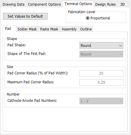
DipTrace remembers the parameters set for the previous package of the same family. You can enter new values or press Set Values by Default button to reset defaults for the given tab.
5.3.2.3.1.4. Design Rules
Clearance values for the footprint elements (silk to pad, courtyard to pad) are set in the Design Rules tab.
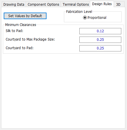
DipTrace remembers the parameters set for the previous package of the same family. You can enter new values or press Set Values by Default button to reset defaults for the given tab.
5.3.2.3.1.5. 3D Model
In 3D tab you can adjust parameters for 3D model generation.
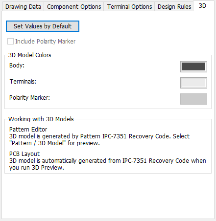
In Pattern Generator, footprints are created with 3D models. Those models are generated based on IPC-7351 Recovery Code in 3D preview mode both in Pattern Generator and PCB Layout modules.
5.3.2.3.2. DIP
5.3.2.3.2.1. Drawing Data
To Generate a DIP package, select Through Hole device type, DIP family.
Check the images to find the required parameters in the datasheet.
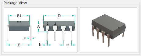
Fill in the red cells in the Drawing Data tab. DipTrace inserts calculated values in the non-required grey cells. Note that Required values can also be calculated based on the values in the non-required grey cells of the same line.
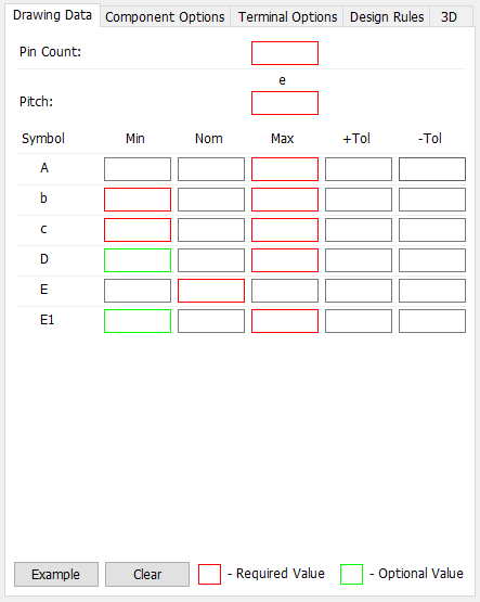
Press Example button to see sample values.
Press Clear button to clear all cells.
5.3.2.3.2.2. Component Options
In Component Options tab you can adjust a number of parameters.
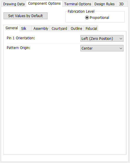
General:
| - | Pin 1 Orientation (Left, Up, Right, Down) |
| - | Pattern Origin (Center, Pin 1) |
Silk:
| - | With Include Silk option activated the software will create Silk Screen shapes for the pattern. Select Package dimensions to be used (min., nom., max.) and set the line width. |
| - | You can also choose to include Pin 1 Marker Line and/ or Dot with user-defined diameter. |
Assembly:
| - | You can choose to include or not the Assembly layer. If included, you can select Package Dimensions (maximum, nominal, minimum) and set the Line Width. |
| - | Add or remove Polarity Marker for polarized components. |
Courtyard:
| - | You can choose to include or not the Courtyard layer. If included, you can set the Line Width for the Courtyard shape; Shape Dimensions are set based on Courtyard to Maximum Package size/ to Pad value from the Design Rules. |
| - | Add or remove Origin Cross for the shapes in the Courtyard layer. |
| - | Add or remove Origin Target for the shapes in the Courtyard layer. |
Outline:
| - | You can choose to include or not the Component Outline. If included, you can set the Line Width for the Outline shape; the shape will be drawn by Nominal Values from the Drawing Data. |
Fiducial:
| - | Placing fiducial is not applicable for this Family. |
DipTrace remembers the parameters set for the previous package of the same family. You can enter new values or press Set Values by Default button to reset defaults for the given tab.
5.3.2.3.2.3. Terminal Options
In the Terminal Options section you can define all the parameters of the pads: their shape (round, square, rounded square), the shape of the first pad (round, square, rounded square), pad corner radius for Rounded Square pad shape, custom solder mask swell, the way to display pads and holes in the assembly layer (don’t show/ contour/ filled shape); you can also choose to include or not the Terminal Outline.
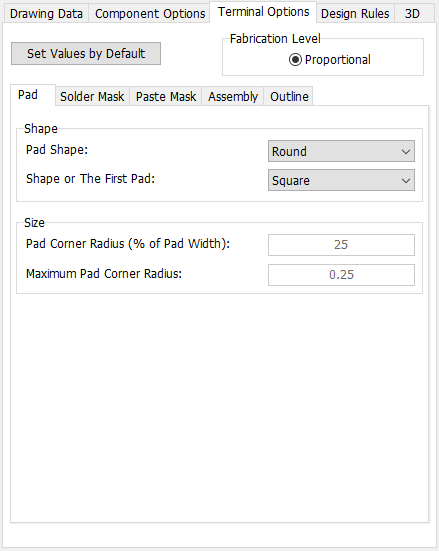
DipTrace remembers the parameters set for the previous package of the same family. You can enter new values or press Set Values by Default button to reset defaults for the given tab.
5.3.2.3.2.4. Design Rules
Clearance values for the footprint elements (silk to pad, courtyard to pad) are set in the Design Rules tab.
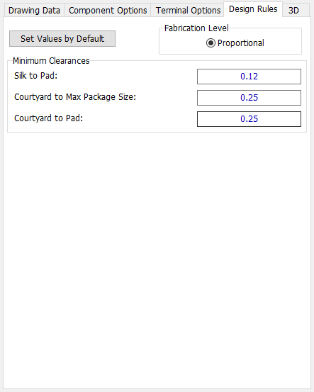
DipTrace remembers the parameters set for the previous package of the same family. You can enter new values or press Set Values by Default button to reset defaults for the given tab.
5.3.2.3.2.5. 3D Model
In 3D tab you can adjust parameters for 3D model generation.
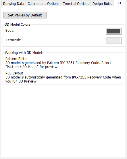
In Pattern Generator, footprints are created with 3D models. Those models are generated based on IPC-7351 Recovery Code in 3D preview mode both in Pattern Generator and PCB Layout modules.
5.3.2.4. Pad Dimensions
Use Calculated Pattern Dimensions - select this option to use of the dimensions of the pads calculated by the software algorithm.
Pattern Dimensions Recommended by Manufacturer - select this option to enter the values recommended by the device vendor.
Check Terminal View images to find the corresponding values in the datasheet.
5.3.2.5. Setting Component Name
Select Use Standard Pattern Name to call a pattern using standard nomenclature.
Choose Use Unique Pattern Name to give a pattern a customized name. If you select this option, you should also specify a Manufacturer, otherwise the software will not create the component.
5.3.2.6. Manufacturer
If you want to add the information about the device manufacturer to the pattern properties, choose a Manufacturer from the default list.
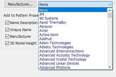
If there’s no required vendor or you want to create your own list of manufacturers, press  button - the following dialog will pop-up:
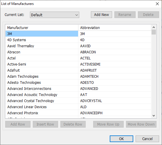
Press  button to add a new list. Press Rename button to give Name to the list.
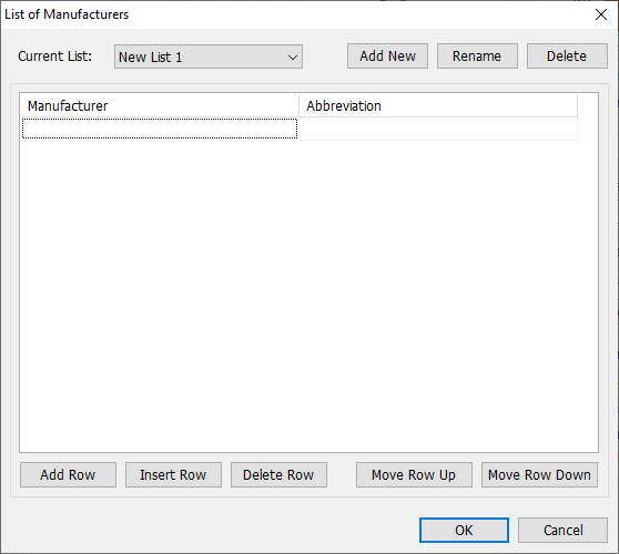
To delete a list, select it from the drop-down and press Delete button.
Use buttons at the bottom of the window to manage the list:
Add Row – create a row at the end of the list.
Insert Row – create a row above the selected line.
Delete Row – remove a row from the list.
Move Row Up – move a row above the previous one.
Move Row Down – move a row below the next one.
5.3.2.7. Add to Pattern Properties
Tick the following items, if you want them to appear in Pattern Properties.
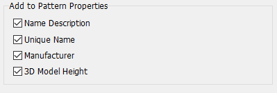
Name Description – add Name Description name to Pattern Properties.
Unique Name – add unique pattern name to Pattern Properties; you should select Use Unique Pattern Name and define it first.
Manufacturer – specified device manufacturer will be added to Pattern Properties.
3D Model Height – with this item checked the value Amax from Drawing Data tab will be automatically added to 3D model dialogue, as Model Height for the By Component Outline option.
5.3.3. Additional fields
Pattern has three standard fields (RefDes, Value, Manufacturer and Datasheet). Besides, you can add a name description and unique name as well as include unlimited number of additional fields for convenience. There are 2 types of additional fields: Texts and Links. Text may contain any textual information and can be used in the same way as standard fields in the PCB Layout (or as search tags). Links may include links to websites. Just right-click on the pattern in the PCB Layout, select Links and open any of pattern internet links.
To add/change default additional fields, which will be applied to all patterns, select "Pattern \ Default Additional Fields" from the main menu in the Pattern Editor, type in the field name, select its type, press Add button, then press Add to All. If you need to apply additional fields only to new patterns, then do not press Add to All button, and close the dialog box to finalize.
To edit/change additional fields of a current pattern, click Additional Fields button on the Pattern Properties panel.
5.3.4. Common pad properties
Select "Pattern \ Standard Pad Properties" from the main menu or press Standard Pad Properties button on the Pattern Properties panel to change common pad properties.
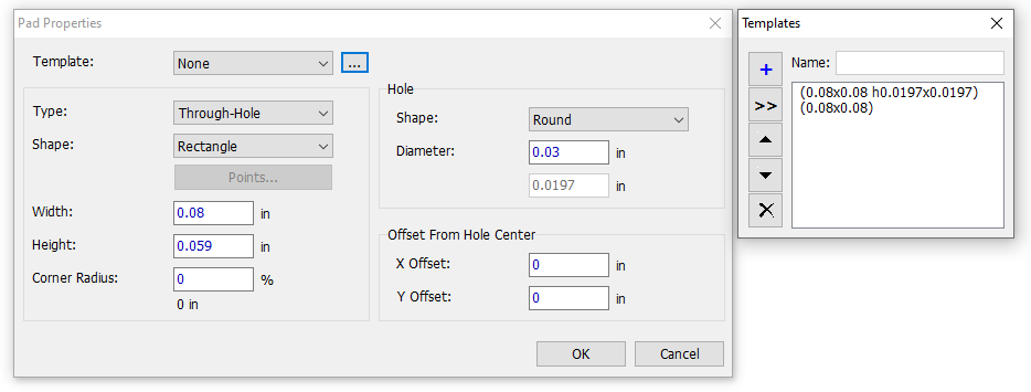
Here you can change properties of the pattern's pad. The parameters are applied to all pads, which use default pattern pad properties.
There are 5 pad shapes: ellipse, obround, rectangle, polygon and D-shape. Pad size is defined by the width and height, you can also specify corner radius for rectangular pads and key points for polygonal pads (press Points button). Through-hole or surface pad type can be selected. For through-hole pad you can define hole shape (round, obround), it’s diameter or width and height as well as X/Y offset of the pad shape from the hole center.
It is possible to set pad properties with a template, just select it from the drop-down list.
To edit templates, press button next to the Template drop-down. Then in the pop-up dialog box you can add a new template with current parameters or edit existing one. To show parameters of existing template, just double click it.
5.3.5. Pads
5.3.5.1. Create
There are 3 ways to create pattern pads:
1. Select pattern style on the Pattern Properties panel (recommended).
2. Placing pads with the mouse: select pad placement tool (single, pad line, pad rectangle or pad circle) from the main menu ("Objects \ Place Pads") or on the Objects toolbar and place them in the design area. Pad-to-pad spacing and pad shape are predefined in the Placement Setup dialog box, select "Objects \ Placement Setup" to open it.
3. Precise placement: select "Objects \ Precise Pad Placement" from the main menu.
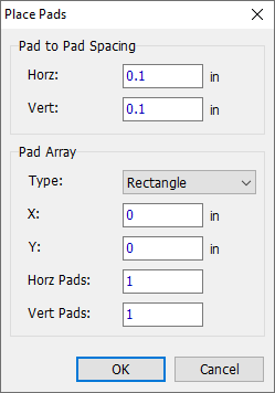
Define "X" and "Y" pad-to-pad spacing, pad shape (single, line, rectangle, or circle), top-left point coordinates, "X" and "Y" number of pads to the bottom-right point, and press OK. All pads will be located in the same signal layer (Top or Bottom).
Pads are created on the current side, selected from the drop-down list on the Objects toolbar. To switch layers you can double-click on the required one in the list on the Layers panel or use T (for Top) and B (for bottom) hotkeys.
5.3.5.2. Edit
There are several pad editing actions:
Moving – change position of the pad (selected pads, shapes, mounting holes and other objects) in the default mode left-click on the pad, and drag it to another location. Alternatively, you can move selected objects using arrow keys of the keyboard.
Aligning objects – select several objects, right-click on one of them and select Align objects from the submenu. In the pop-up, define, how you want the objects to be aligned relative to each other (horizontally or vertically, by top/center/bottom or distributed equally).
Rotation – rotate a pad, right-click it, and select Rotate from the submenu or select pad, and press R or Space. All selected pads will be rotated 90 degrees counter-clockwise. To set a different rotation angle, double-click on a pad or right-click on it and select Pad Properties from the submenu. In Number/Position tab of the pop-up, type-in Pad Angle value.
Changing Mask/ Paste Settings for individual pads – pads can have custom properties in the solder mask and paste layers. Right-click on the pad, and select Mask / Paste Settings to change custom pad solder mask/paste properties.
Defining individual Pin Terminal parameters – right-click on a pad and select Pin Terminal from the submenu; define pin terminal shape type (obround, rectangle, polygon, D-shape), its size, X and Y offset relative to the pad shape and rotation angle for the Current Pad, Similar Pads, Selected Pads or All Pads of the current pattern.
Changing side – change the side of selected pads, right-click on one of them, and select Change Side from the submenu.
Deleting – delete pad, right-click it, and select Delete from the submenu or select pad, and press Del key. All selected objects will be deleted.
5.3.5.3. Properties
To change pad properties, right-click on the pad, and select Properties from the submenu. The following dialog will appear:
|
|
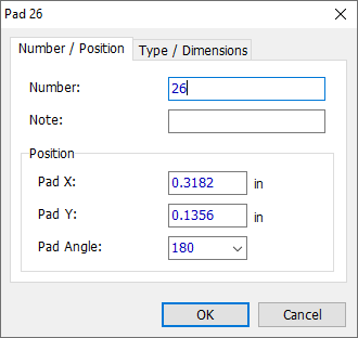
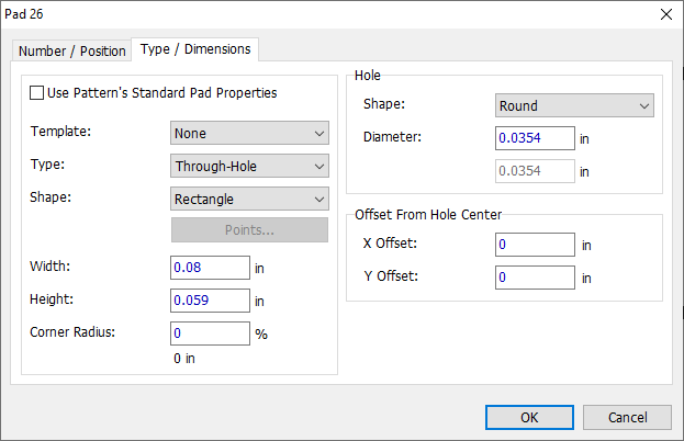
Here you can change pad number, note, coordinates, and orientation. If you export schematic to PCB or place pattern in the PCB Layout, component pin names become pattern's pad notes.
Use Pattern's Standard Pad Properties box means that default pad settings from the Standard Pad Properties dialog box are applied to this pad automatically. Uncheck this item to allow for custom settings.
Pad properties templates can be used. Use Standard Pad Properties dialog box to create and edit templates.
Pads can be through-hole or surface, for through-hole pads you can define the hole type and dimensions. There are 5 pad shapes: ellipse, obround, rectangle, polygon and D-shape. Pad size is defined by the width and height, you can also specify corner radius for rectangular pads and key points for polygonal pads (press Points button). For through-hole pad you can define hole shape (round, obround), it’s diameter or width and height as well as X/Y offset of the pad shape from the hole center.
5.3.5.4. Pad array numbers
Automated pad renumbering feature (applied with pattern types) allows the designer to create correct complex footprints in few seconds.
Select all pads of the pattern, right-click on the first pad (first pad is important for contour numeration, i.e. for any DIP/SOIC or QUAD type footprints), choose Pad Array Numbers from the submenu, the following dialog box will pop up:
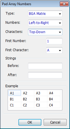
Here you can select type of the numeration: Linear matrix, Contour and BGA Matrix.
Each type of numeration has its own parameters displayed below the type field. You can preview results of the future numeration in the Example field.
For contour type numeration it is important that you click on the pad that should be the first when called this dialog box.
5.3.5.5. Mask and paste
Default solder mask and paste settings for all pads on the circuit board are defined in the Gerber export dialog box in the PCB Layout. However, pads can have custom properties in the solder mask and paste layers. Right-click on the pad, and select Mask / Paste Settings to change custom pad solder mask/paste properties.
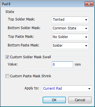
Select the state of the top/bottom solder mask/paste of the pad, using respective drop-down lists in the State section of the dialog box.
Common state – apply default solder mask and solder paste parameters to the pad;
Open – pad not covered with solder mask regardless of the default parameters;
Tented – pad covered with solder mask regardless of the default parameters;
Solder – apply solder paste to the pad regardless of the default parameters;
By Paste Mask – solder mask will match Paste Mask;
No Solder – do not apply solder paste to the pad regardless of the default parameters;
Segments – a useful option for big pads, which allows splitting paste into segments instead of filling the entire pad area. With this option selected you can define fill percent, min. segment side, min.segment gap and nominal edge gap for the paste mask segments.
If you need custom solder mask swell and paste mask shrink settings for the pad/s, check the respective check boxes and enter custom values (negative numbers are supported).
Changes can be applied to the current pad, to all similar pads, or to selected pads.
5.3.6. Shapes
5.3.6.1. Create
There are two ways to add shape to the footprint drawing:
1. Place with the mouse pointer: select the shape placement tool from the main menu ("Objects \ Place Shape") or select it on the Drawing toolbar and specify key points on the pattern design area. To facilitate shape placement DipTrace displays shape’s dimensions during drawing.
2. Precise Placement: select "Objects/ Precise Shape Placement" from the main menu, define shape type, placement layer, line width, dimensions, start and end points (for lines and arcs), key points (for polylines and polygons), and anchor point locations, then press OK.
Shape placement layer can be predefined with the drop-down list on the Drawing toolbar. However, you can change the layer of existing shape in the Shape Properties dialog box selected from the shape's right-click submenu.
Text object is similar to a shape but has slightly different properties in the right-click submenu (Font, Font Type, Show etc.).
5.3.6.1.1. Line
To place a line, press button on the Objects Toolbar. Left-click to anchor the starting point and the end point. When drawing the line, it’s dimensions will be displayed by DipTrace.
Alternatively, you can use Precise Shape Placement dialog, launched from the Objects menu or by pressing Ctrl + F hotkeys. Select Line from the Shape Type drop-down.
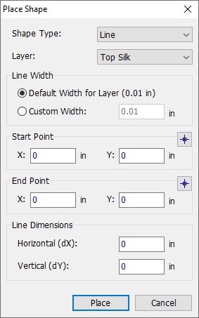
Choose the Layer, where you want a Line to be placed to. If Top or Bottom layer is selected from the list, All Signal Layers checkbox becomes active; tick it if you want a shape to be placed both on Top and Bottom layer. You can choose to use Default Line Width for the selected layer or type-in a custom value in the respective cell. You can define Start and End Points by X and Y coordinates or use  button to set them by Mouse Pointer. Next, type-in line dimensions by X and/or Y axis. Click Place.
5.3.6.1.2. Arc
To place an Arc, press  button on the Objects Toolbar. There are three modes for Arc placement in DipTrace. Left-click to anchor the starting point, then right-click to select the mode:
Start - Center - Angle - with this mode selected an arc with a certain angle is built based on a circle with defined radius. Anchor the starting point, the center point of a circle will appear; the radius of the circle is equal to the distance between the starting point and the center point. Move the center point away from the starting point to get a circle with desired parameters. Next left-click and adjust the angle of the arc. Left-click to anchor the end point of the arc.
Start - End - Radius - in this mode an arc of desired radius is built between the Start and End points. Place the Start and End Points and move the mouse pointer to adjust the radius of the arc. Left-click when done.
Start - End - Middle Point - in this mode an arc is built based on three points. Place Start and End point, the third point will appear on the line between them. Move the point to get an arc with desired parameters.
Choose Clockwise or Counter-Clockwise from the right-click submenu to set the concavity direction of the curve.
Select Cancel from the right-click submenu to cancel the arc placement.
When drawing an arc, it’s key parameters (radius, deg.) will be displayed by DipTrace.
Alternatively, you can use Precise Shape Placement dialog, launched from the Objects menu or by pressing Ctrl + F hotkeys. Select Arc from the Shape Type drop-down.
|
|
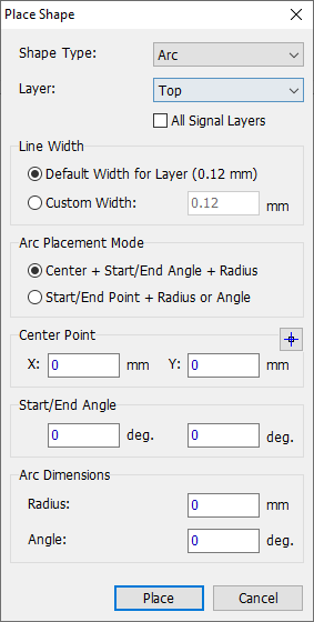
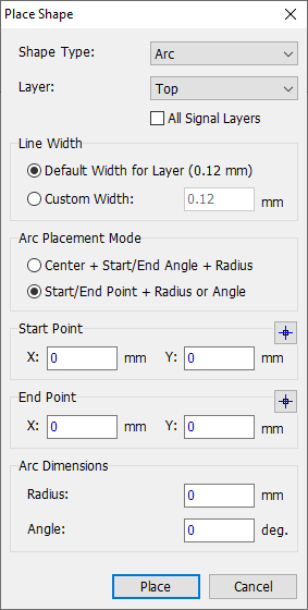
Choose the Layer, where you want an Arc to be placed to. If Top or Bottom layer is selected from the list, All Signal Layers checkbox becomes active; tick it if you want a shape to be placed both on Top and Bottom layer. You can choose to use Default Line Width for the selected layer or type-in a custom value in the respective cell.
Select an Arc placement mode. And type-in all the required values. Note that points can be defined by X and Y coordinates or set by Mouse Pointer upon pressing . Press Place button.
5.3.6.1.3. Rectangle/ Filled Rectangle
To place a Rectangle/ Filled Rectangle, press  or
or  button respectively on the Objects Toolbar. Left-click to anchor the starting point, draw the shape and left-click in the end point. When drawing the shape, it’s dimensions will be displayed by DipTrace.
Alternatively, you can use Precise Shape Placement dialog, launched from the Objects menu or by pressing Ctrl + F hotkeys. Select Rectangle/ Filled Rectangle from the Shape Type drop-down.
|
|
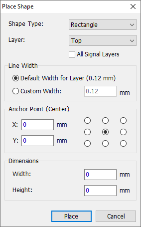
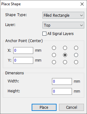
Choose the Layer, where you want a Rectangle/ Filled Rectangle to be placed to. If Top or Bottom layer is selected from the list, All Signal Layers checkbox becomes active; tick it if you want the shape to be placed both on Top and Bottom layer. You can choose to use Default Line Width for the selected layer or type-in a custom value in the respective cell.
Next, you can choose the position of an anchor point and type-in its coordinates. Define shape dimensions and press Place button.
5.3.6.1.4. Obround/ Filled Obround
To place a Obround/ Filled Obround shape, press  or
or  button respectively on the Objects Toolbar. Left-click to anchor the starting point, draw the shape and left-click in the end point. When drawing the shape, it’s dimensions will be displayed by DipTrace.
Alternatively, you can use Precise Shape Placement dialog, launched from the Objects menu or by pressing Ctrl + F hotkeys. Select Rectangle/ Filled Rectangle from the Shape Type drop-down.
|
|
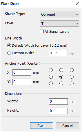
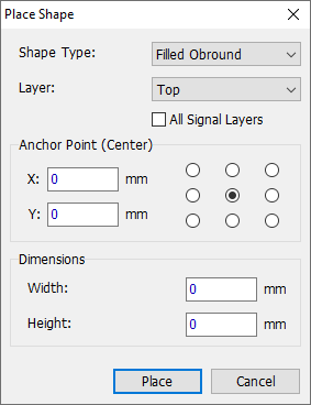
Choose the Layer, where you want a Obround/ Filled Obround shape to be placed to. If Top or Bottom layer is selected from the list, All Signal Layers checkbox becomes active; tick it if you want the shape to be placed both on Top and Bottom layer. You can choose to use Default Line Width for the selected layer or type-in a custom value in the respective cell.
Next, you can choose the position of an anchor point and type-in its coordinates. Define shape dimensions and press Place button.
5.3.6.1.5. Polyline/ Polygon
To place a Polyline/ Polygon, press  or
or  button respectively on the Objects Toolbar. Left-click to anchor the starting point, draw the shape, left-click to anchor points, right-click in the end point and select Enter form the submenu. When drawing the shape, it’s dimensions will be displayed by DipTrace.
Alternatively, you can use Precise Shape Placement dialog, launched from the Objects menu or by pressing Ctrl + F hotkeys. Select Polyline/ Polygon from the Shape Type drop-down.
|
|
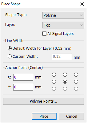
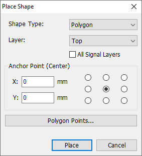
Choose the Layer, where you want a Polyline/ Polygon to be placed to. If Top or Bottom layer is selected from the list, All Signal Layers checkbox becomes active; tick it if you want the shape to be placed both on Top and Bottom layer.You can choose to use Default Line Width for the selected layer or type-in a custom value in the respective cell.
Next, you can choose the position of the anchor point and type-in its coordinates. Define Polyline/ Polygon key points by pressing Polyline Points/ Polygon Points button respectively.
|
|
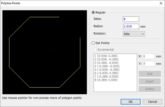
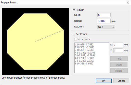
Press Place button to create a shape.
5.3.6.2. Edit
There are the following functions for editing shapes:
Moving – change shape position in the default mode. Hover over the shape (not over its key points) with the mouse, and drag it.
Aligning objects – select several objects, right-click on one of them and align objects respectively to each other horizontally or vertically.
Changing the size – change shape size, hover over the key point of the shape with the mouse, and drag it to a new location. You can change shape size in the Shape Properties dialog boxes (right-click submenu / Properties).
Rotation – rotate shape 90 degrees counter-clockwise, right-click on the shape, and select Rotate from the submenu or select the shape, and press R.
Changing layer – right-click on a shape, and select Properties from the submenu. Then make changes in the Layer drop-down list.
Deleting – delete shape or text, right-click it, and select Delete from the submenu or just select shape, and press Del key. All selected objects will be deleted. It is possible to delete objects by completely deleting a logical layer containing them.
5.3.6.3. Properties
Right-click on the shape, and select Properties from the submenu to open the Shape Properties dialog box:
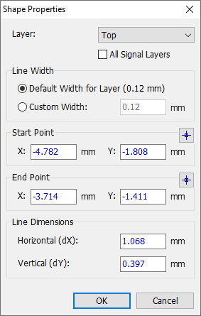
Here you can change shape's type (Top Assy, Top Silk, Top Mask, Top Paste, Top, Bottom, Route Keepout, Bottom Paste, Bottom Mask, Bottom Silk, Bottom Assy or Board Cutout), shape point coordinates and line width.
5.3.6.3.1. Line
Right-click on a line, and select Properties from the submenu to open Shape Properties dialog box:
Here you can change the shape Layer.
If Top or Bottom layer is selected from the list, All Signal Layers checkbox becomes active; check it if you want the shape to be placed both on Top and Bottom layers. Additionally, the Connected Pad drop-down list appears, allowing you to connect the shape to any pad of the pattern, this helps avoid DRC errors, caused by overlapping shapes and pads on the same conductor layer.
You can choose to use default line width for the selected Layer; or customize it for the given shape.
Start and End Points can be adjusted by changing X and Y coordinates or by using button to set them by Mouse Pointer.
Finally, you can edit Line Dimensions, just type-in new values for Horizontal (dX) and Vertical (dY) tangent.
5.3.6.3.2. Arc
Right-click on an Arc, and select Properties from the submenu to open Shape Properties dialog box:
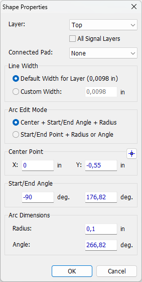
Here you can change the shape Layer.
If Top or Bottom layer is selected from the list, All Signal Layers checkbox becomes active; tick it if you want the shape to be placed both on Top and Bottom layers. Additionally, the Connected Pad drop-down list appears, allowing you to connect the shape to any pad of the pattern, this helps avoid DRC errors, caused by overlapping shapes and pads on the same conductor layer.
You can choose to use default line width for the selected Layer; or customize it for the given shape.
Select an Arc Edit mode: Center+Start/End Angle+Radius or Start/ End Point+Radius or angle. Type-in all the required values. Note that points can be defined by X and Y coordinates or set by Mouse Pointer upon pressing .
Finally, you can change arc Radius and Angle.
5.3.6.3.3. Rectangle/ Filled Rectangle
Right-click on a Rectangle/ Filled Rectangle, and select Properties from the submenu to open Shape Properties dialog box:
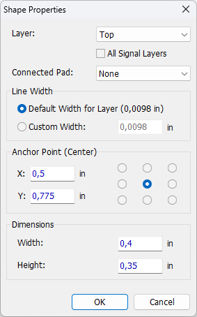
Here you can change the shape Layer.
If Top or Bottom layer is selected from the list, All Signal Layers checkbox becomes active; tick it if you want the shape to be placed both on Top and Bottom layers. Additionally, the Connected Pad drop-down list appears, allowing you to connect the shape to any pad of the pattern, this helps avoid DRC errors, caused by overlapping shapes and pads on the same conductor layer.
You can choose to use default line width for the selected Layer; or customize it for the given shape.
Next, you can change the position of an anchor point and type-in its coordinates.
Finally, you can edit shape dimensions.
5.3.6.3.4. Obround/ Filled Obround Prop
Right-click on an Obround/ Filled Obround shape, and select Properties from the submenu to open Shape Properties dialog box:
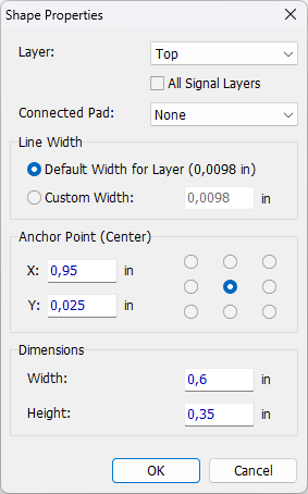
Here you can change the shape Layer.
If Top or Bottom layer is selected from the list, All Signal Layers checkbox becomes active; tick it if you want the shape to be placed both on Top and Bottom layers. Additionally, the Connected Pad drop-down list appears, allowing you to connect the shape to any pad of the pattern, this helps avoid DRC errors, caused by overlapping shapes and pads on the same conductor layer.
You can choose to use default line width for the selected Layer; or customize it for the given shape.
Next, you can change the position of an anchor point and type-in its coordinates.
Finally, you can edit shape dimensions.
5.3.6.3.5. Polyline/ Polygon
Right-click on a Polyline/ Polygon shape, and select Properties from the submenu to open Shape Properties dialog box:
|
|
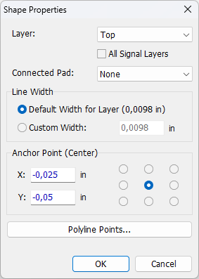
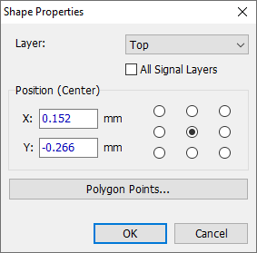
Here you can change the shape Layer.
If Top or Bottom layer is selected from the list, All Signal Layers checkbox becomes active; tick it if you want the shape to be placed both on Top and Bottom layers. Additionally, the Connected Pad drop-down list appears, allowing you to connect the shape to any pad of the pattern, this helps avoid DRC errors, caused by overlapping shapes and pads on the same conductor layer.
You can choose to use default line width for the selected Layer; or customize it for the given shape.
Next, you can change the position of an anchor point and type-in its coordinates.
Finally, you can edit shape dimensions by clicking on Polyline Points/ Polygon Points button.
5.3.7. Text
5.3.7.1. Create
A multiline text can be placed in DipTrace. Go to Objects/ Place Text or press  button on Objects toolbar.
Left-click on the design area and type the text.
Use Enter key to move to the next line.
Right-click in the on a free spot of the design area to return to default mode.
Note that tilde (~) before and after text is reserved by the software for placing a line over the pin name, which implies inversion; if you want a tilde symbol to appear as it is, you should place it twice:
~text~/~~text

5.3.7.2. Edit
To edit, double click on the text object or right-click on it and select Edit Text. The following dialog will appear:
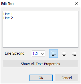
Here you can change the text, line spacing and alignment. Press Show All Text Properties button to access Text Properties (link Pattern Editor > Designing the pattern > Text > Properties) dialog that allows for adjusting more text object parameters.
Hover over a text object and drag it to another location.
To delete a text, right-click it, and select Delete from the submenu.
5.3.7.3. Properties
To open Text Properties dialog, right-click on the text object and select Properties from the submenu.
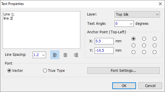
In the pop-up dialogue you can set line spacing, text alignment and font, define its type, and choose a 90-fold angle from the drop-down or just type-in the required value to rotate the text.
The location of the Anchor Point of the text box is set by ticking the respective circle. Anchor Point is displayed as a cross. You can also set the coordinates of the Anchor point.
Press Font Settings button to open Font dialog (it can also be accessed by selecting Font in the text right-click submenu):
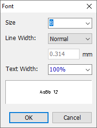
Here you can set the font size, select the Line Width from Thin, Normal, Bold or Customize it, and also define the Text Width.
5.3.8. Mounting hole
Mounting hole is defined only by 2 parameters: hole (inner) diameter and outer (keepout area) diameter.
There are two ways to place mounting holes:
1. With the mouse pointer, select "Objects \ Place Mounting Hole" from the main menu or press button on the Objects toolbar, and left-click on the pattern design area.
2. Precise Placement, select "Objects \ Precise Hole Placement" from the main menu, define the coordinates, diameters, and press OK.
To define mounting hole diameters before placement, use Placement Setup dialog box.
To change the diameter of existing hole, right-click it, and select Properties from the submenu. This dialog box also allows the user to precisely change the hole's position.
Hover over the mounting hole and drag it to another location.
To delete a mounting hole, right-click it, and select Delete from the submenu.
5.3.9. Fiducial
A fiducial is defined by two parameters: copper and keepout area diameters.
To place a Fiducial select "Objects/ Place Fiducial" from the main menu or press button on the Objects toolbar. Left-click on the design area to place a fiducial.
Fiducial name, position coordinates, and copper/ keepout diameters can be set in the Properties dialogue launched via right-click submenu.
Hover over the fiducial and drag it to another location.
To delete a fiducial, right-click it, and select Delete from the submenu.
5.3.10. Dimensions
You can place four types of dimensions (horizontal, vertical, free, radius) and a pointer (displays point coordinates or any custom text).
Dimensions or pointer can be attached to any object's key points. It is moved/resized automatically when editing or moving an object.
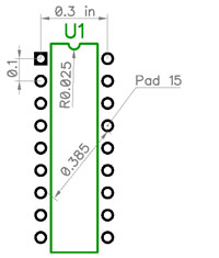
Select "Objects \ Place Dimension \ <Dimension Type>" from the main menu or press  button on the Objects toolbar, then left-click on the first point (key points are highlighted automatically) or arc (if you measure the radius), and then left-click on the second point (if necessary), and choose the dimension's position.
Dimensions can be disconnected or connected from/to the key points with the right-click submenu. You can change/display dimension's units and change other properties in the "right-click submenu \ Properties" item.
5.3.11. 3D model
DipTrace allows the user to preview circuit boards in three dimensions with all components installed. In order to see components on the circuit board, patterns should have attached 3D models. You can connect 3D models in PCB Layout, but we recommend doing this in Pattern Editor to have a complete component.
Press 3D model button on Pattern Properties panel or select "Pattern/ 3D Model" from the main menu to access 3D Model dialog.
There three ways to add a 3D model to a component package.
1. Load 3D Model file. Select 3D Model File option from a drop-down. Press All Models >> button to open the list of all available 3D models in active library. Select a model from the list, and preview it immediately (3D models in the list are organized by pattern libraries).
VRML and STEP 3D models are in different categories with the same title.
Press button, and select any 3D model file on your computer, or type in its address, and press Load Model button. DipTrace supports *.3ds, *.wrl, *,step, and *.iges 3D model files which are often available online on the manufacturers' websites.
Use a corresponding section of this dialog box to adjust 3D model's location respective to the footprint by changing shift, angle and scale by each axis (enter new values into the corresponding fields).
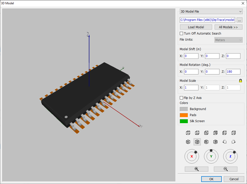
2. IPC-7351 Model Generator. This option is available only if Pattern Generator was used to make a footprint.
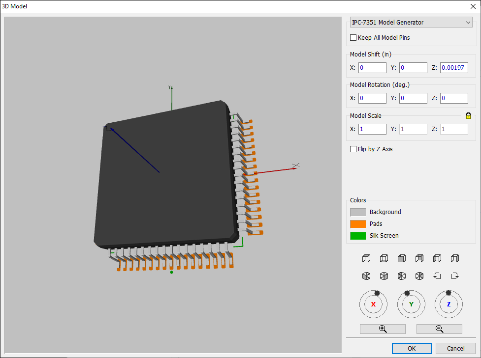
| 3. | Create a 3D model by Component Outline. To use this option, an outline has to be placed first. Go to Objects/ Precise Shape Placement and place a shape in the Top Outline layer (the size should be equal to or a bit smaller than the silk screen shape). Specify the model height and DipTrace will generate a 3D shape to mimic a device. This option can also be used if there is no 3D model for a footprint designed in the generator. |
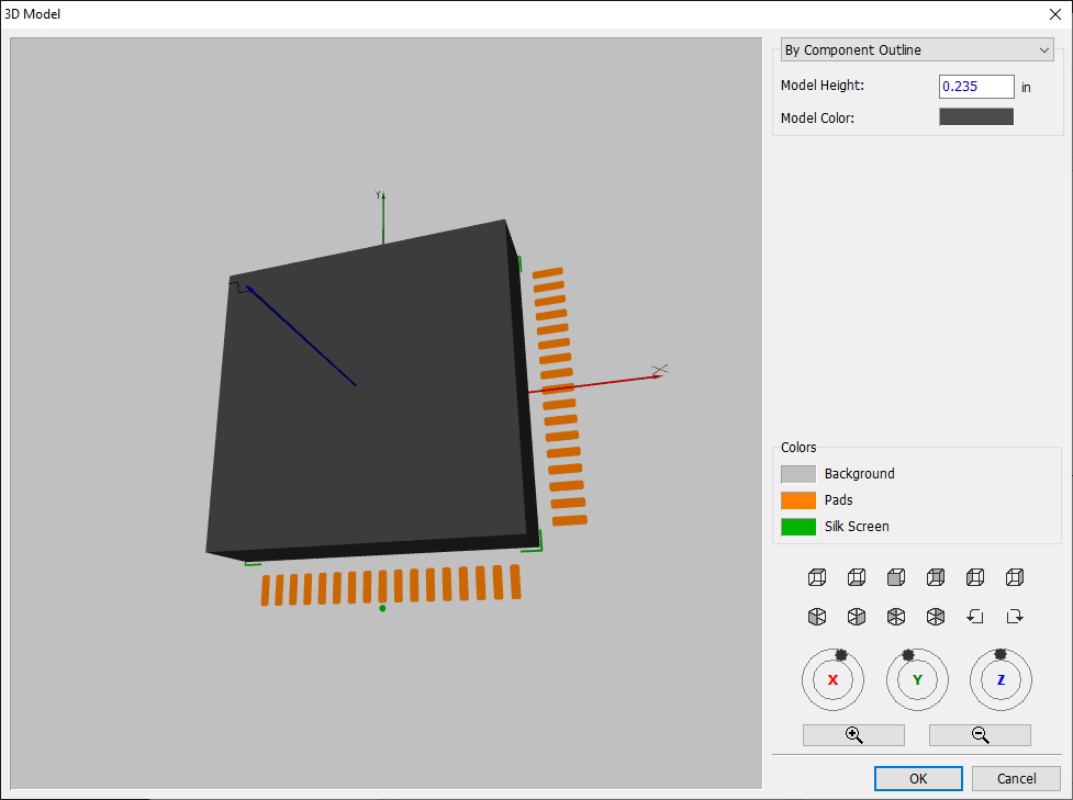
For a better preview, change a color of the background, pads or silk layer (just click on the corresponding color rectangle).
To rotate/move/zoom electronic component in the preview area:
1. Hold down the left mouse button to rotate around X or Y axis. Hold down the mouse wheel (middle button) to rotate around Z axis.
2. Hold down the right mouse button to pan.
3. Mouse wheel Up or Down to Zoom In/Out.
Use side and isometric view buttons for quick change of 3D display perspective.
Rotate and Zoom is also possible with the tools on the right side of the screen.
5.3.12. Align objects
Select objects on the design area, then go to "Edit \ Align Objects" from the main menu, or right-click on one of the objects and select Align Objects from the submenu.
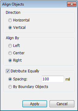
Select the alignment direction, then select how to align objects in the row or column (left, center or right) and set distribution settings by objects' boundaries or equally with a custom spacing.
You need to select at least two objects to have the Align tool available, because the alignment is relative.
5.3.13. Edit pattern
Pattern Editor has the following general editing functions for patterns:
Center pattern with respect to the origin point. Select "Edit \ Center Pattern" from the main menu or press Ctrl+Alt+C.
Rotate pattern 90 degrees clockwise. Select "Edit \ Rotate Pattern" from the main menu or press Ctrl+Alt+R.
Flip pattern vertically with respect to X axis. Select "Edit \ Vertical Flip" from the main menu or press Ctrl+Alt+V.
Flip pattern horizontally with respect to Y axis. Select "Edit \ Horizontal Flip" from the main menu or press Ctrl+Alt+H.
5.3.14. Placement setup
To change default pad and mounting hole parameters before placement, select "Objects \ Placement Setup" from the main menu. The following dialog box pops up:
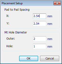
Here you can change X and Y pad-to-pad spacing for pad shapes.
For the mounting hole it is possible to define hole (inner) and outer (keepout area) diameters.
5.3.15. Insert from library
To insert pattern from the pattern or component library, select "Pattern \ Insert from Another Library" or press Get from Library (  ) button on the Pattern Properties panel.
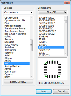
In the pop-up dialog box, select a library and component in the corresponding lists. Use library groups and search filters for convenience. Press Library Setup button to edit the library groups. Preview field available.
5.3.16. Import from DXF
DipTrace allows the designer to import a whole component pattern or its part from a DXF file.
To import DXF file, select "Pattern \ Import from DXF" from the main menu in the Pattern Editor, then select and open existing DXF file.
In the pop-up dialog box you can preview selected DXF file and specify connections between the DXF and DipTrace PCB layers. To set connection between DXF and PCB layers, select layer from the DXF layers list, and a corresponding DipTrace layer in the Convert to drop-down list.
To show/hide different layers of the DXF file, click on the first column of the Layers table (blue check marks).
Notice that import feature has recognition options, i.e., for example, if you have pad shapes in one DXF layer and all drills (including the mounting holes) in another layer, then specify "Pads" for the first layer and "All Holes" for the second layer. You will get through-hole pads with holes inside pad shapes, surface pads without holes and mounting holes (without shapes).
DipTrace can Fill Closed Areas and recognize polygons embedded, check respective check boxes in the Import DXF dialog box.
5.4. View functions
5.4.1. Scaling/Panning
There are several ways to change the scale of design area:
1. Mouse wheel – you can decrease or increase the scale in very wide limits.
2. Drop-down list on the Standard toolbar (from 25% to 800%).
3. "View \ Scale" from the main menu. It is possible to select from 25% to 800%, zoom in, zoom out or specify custom scale.
4. Pressing the Plus sign (+) key to zoom in or Minus sign (-) key to zoom out.
5. Zoom window tool on the Standard toolbar allows for zooming to the box defined with the mouse pointer.
Current scale is always displayed in the drop-down list on the Standard toolbar.
Pan design area with the right mouse button (hold down and move) or by arrow keys while creating the shape etc.
5.4.2. Line Width
In the fly-out window you can set the default width of the lines for the shapes placed in different layers (Silk, Component Outline, Courtyard, Board Cutout, Other Layers).
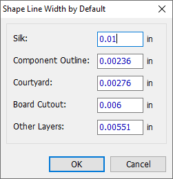
The width of the lines of individual shapes can be customized in Shape Properties dialogue accessed by selecting Properties from the right-click submenu.
5.4.3. Precision
DipTrace allows adjusting the precision rate for project values and the grid.
Select View/ Precision… to open the following dialogue-box:
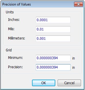
Configure the precision level by defining the number of decimal places (up to ten) for all the values used in the project by units.
You can also set the minimum grid size and grid precision for the current units. Those values are converted, when measurement units are changed.
Please note that high precision rates are used only at designing stage. When the project is saved into a file, precision up to 0.001 mil is applied.
5.4.4. Grid
DipTrace Pattern Editor allows the user to create and edit objects free or according to the grid.
To show/hide the grid, select "View \ Grid" from the main menu or press F11 hotkey.
Select "View \ Snap to Grid" from the main menu, or press Alt+F11 hotkey (by default) to activate/deactivate snap to grid, when the grid is on.
If Snap to Grid option is disabled, objects are no longer snapped to the grid, but you can leave the grid visible.
When Snap to Grid option is disabled for the entire project, you can choose to snap to grid individual elements of your pattern (pad, shape, text, image, etc.) by selecting Snap to Grid item from the right-click submenu of those elements, when the grid is on.
Select "View \ Grid Size" from the main menu to open the grid size submenu. You can select standard or specify custom grid size.
It is possible to select grid size from the list on the Standard toolbar or just press Ctrl + Plus sign (+), Ctrl + Minus sign(-) hotkeys to change the grid.
To change the list of predefined grid sizes, select "View \ Customize Grid" from the main menu.
Select "View \ Y Grid Size" from the main menu to set a separate grid step for the vertical axis.
5.4.5. Origin
Origin is customizable, you can change its position at any moment while creating and editing a footprint. Select "View / Display Origin" from the main menu or press F1 hotkey.
Origin can be defined with the mouse pointer or by coordinates (incremental to existing origin). To define it with the mouse, select "View / Define Origin / By Mouse Pointer" from the main menu or press the corresponding button on the Objects toolbar, then define a new origin with a left-click on the design area. To change the origin by coordinates, select "View / Define Origin / By Coordinates" from the main menu.
To return origin to default position (center of the design area) select "View / Define Origin / Default Position".
To change the origin display parameters, select Pattern/ Origin Properties.
To change the color of the axis, select "View / Axis Color" from the main menu.
5.4.6. Pad numbers
In the Pattern Editor you can display pad numbers and even define their font. To display pad numbers, select "View \ Pad Numbers \ Show" from the main menu.
Font can be assigned automatically, based on the pad size or set manually by selecting "View \ Pad Numbers \ Font" from the main menu.
5.5. Working with layers
5.5.1. Review
All signal and non-signal layers of the pattern are available on the Layers panel on the right side of the screen.
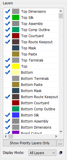
To select a layer, double-click it in the list.
To show/hide a layer on the design area, click on the corresponding blue check mark in the list. To change layer color, left-click on the color rectangle. Notice that the color of the pattern constituents depends on the layer color.
By default all layers are sorted from the top side of the pattern to the bottom. However, you can arrange them in the order you prefer and choose priority layers to be displayed in the list, with all other layers hidden. Press button to open Layer Priority and Order dialog.
Tick the layers you want to be displayed in priority list; use  and
and  buttons to change their order in the list.
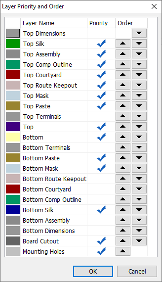
Press Show Priority Layers Only button to display only pre-established priority layers.
Press Show All Layers button to display all layers.
Use Display Mode drop-down to choose among the following layer display modes:
1. Current Only – only the active signal layer is visible. Double-click on the layer in the Layers tab to select an active layer.
2. All Layers – all signal layers are visible. We recommend setting different colors for the layers.
3. Contrast – only active layer is at full contrast, other PCB layers are visible with reduced contrast. Go to "View \ Layer Display \ Contrast Level" or press button on the Layers tab to adjust the contrast level.
Press  to adjust contrast levels applied in the Contrast display mode.
5.6. Edit functions
5.6.1. Select objects
Objects should be selected if you want to edit or remove them. DipTrace has several ways to select objects or edit existing selection:
Way 1. Click on the object with any of the mouse buttons. Use the left mouse button to select an object, and the right mouse button to open the object's submenu.
Way 2. In the Default mode hold down the left mouse button on an empty area and move the mouse cursor – selection box will appear. All objects inside this box will be selected when you release the mouse button.
To invert object selection, press Ctrl key, and select objects. To add objects to the selection, use the Shift key.
To select all pattern objects, go to "Edit \ Select All" from the main menu.
Way 3. Edit Selection dialog box allows the user to select objects by type and parameters. Several modes are available: new selection, add to selection, remove from selection, keep selected.
Choose "Edit \ Edit Selection" from the main menu.
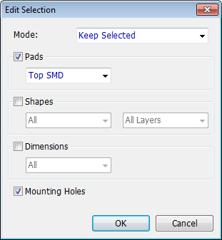
In the pop-up dialog box select objects and define the selection mode. The following modes are supported:
1. New Selection – deselect all previously selected objects and create a new selection, based on your choice;
2. Add to Selection – add specified objects to existing selection;
3. Remove from Selection – remove specified objects from existing selection;
4. Keep Selected – select objects by type and area. Use box selection and Ctrl key to define a selection area (see Way 2), then select Keep Selected to remove unspecified objects from the selection. Only the objects specified in this dialog box will remain selected on the exact area.
5.6.2. General functions
There are the following general editing functions: Delete, Cut, Copy, and Paste.
Select objects before applying these functions.
To apply one of these functions to objects, select the corresponding sub-item from the main menu ("Edit"). It is possible to use hotkeys: Cut (Ctrl+X), Copy (Ctrl+C), Paste (Ctrl+V), and Delete (Del).
5.6.3. Undo/Redo
To cancel the last editing step and return to the previous state, select "Edit \ Undo" from the main menu or press the corresponding button on the Standard toolbar.
It is also possible to recover canceled steps. Choose "Edit \ Redo" from the main menu or press the corresponding button on the Standard toolbar. If you edit symbol after using the Undo tool, Redo tool becomes inactive.
5.6.4. Move/Rotate objects
To change location of some objects select them, and drag to a new location.
To rotate objects counter-clockwise, select them first, then press R key or select "Edit \ Rotate" from the main menu.
Rotate or flip several objects as a group with Shift+R and Shift+F hot keys respectively.
5.6.5. Align objects
Select objects on the design area, then go to "Edit \ Align Objects" from the main menu, or right-click on one of the objects and select Align Objects from the submenu.
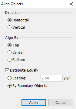
Select the alignment direction, then select how to align objects in the row or column (left, center or right) and set distribution settings by objects' boundaries or equally with a custom spacing.
You can group multiple objects into one so they will stay together if they are aligned or distributed.
At least two objects (or groups of objects) have to be selected for the Align tool to become available because the alignment is relative.
5.6.6. Radial Placement
DipTrace Pattern Editor allows for radial placement of pads, mounting holes and fiducials. Select one or several objects on the design area, then go to "Edit\ Radial Placement" from the main menu, or right-click on one of them and select Radial Placement from the submenu.
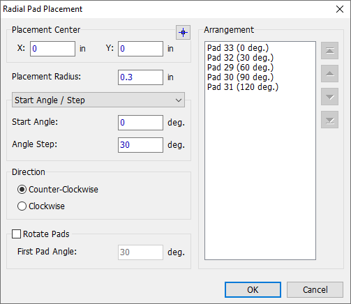
You can enter the coordinates of the point that will be used as placement center or press button and set it with the mouse pointer in the design area.
Enter Placement Radius - the distance between the placement center and the origin point of the object.
Use the drop-down to select how you want the objects to be distributed: based on Start Angle and Step or Start and End Angles.
Define placement Direction - clockwise or counterclockwise.
Mark Rotate Pads and set the First Pad Angle, if you want the objects to be rotated to a certain angle when placed radially.
In the Arrangement section use arrow buttons to change the order of the objects in the array.