

DipTrace Tutorial
This step-by-step tutorial covers the complete PCB design workflow in DipTrace — from schematic capture and component library creation to autorouting, high-speed differential pair routing, and manufacturing output (Gerber X2, ODB++, IPC-2581). DipTrace is professional PCB design software used by over 30,000 engineers worldwide, including aerospace, defense, and medical companies. It is available with a perpetual license (no subscription required), works fully offline, uses an open XML file format, and includes free technical support for all users — including the free version. The tutorial follows a real project from a blank schematic to production-ready files. No prior experience with DipTrace is required.
Creating a simple schematic
1. Creating a simple schematic
4. Establishing schematic size and placing titles
Designing a PCB
10. Autorouting
13. Net classes
14. Manual routing
16. Selecting objects by type/layer
18. Copper pour
19. Locking objects
22. Panelizing
23. Printing
Generating files for manufacturing
24. DXF
25. Gerber RS-274X
26. Gerber X2
28. ODB++
29. Order PCB
30. Creating Component Libraries
31. Designing a pattern library
32. Customizing Pattern Editor
34. Designing a resistor (pattern)
35. Manually
37. Automatically (Pattern Generator)
Designing BGA-144/13x13
38. Manually
39. Designing BGA Automatically
41. Designing a component library
42. Customizing Component Editor
43. Designing a resistor (component)
45. Designing VCC and GND symbols
46. Designing a multi-part component
49. SPICE Model
51. Placing parts
Connecting
54. Net ports
56. Connection Manager in Schematic and PCB Layout
60. Layer stack
High-speed nets and differential signals
61. Length matching
62. Signal delay
63. Create a differential pair
64. Differential pair routing/editing
65. Phase tuning a differential pair
69. Back annotate
72. Saving/loading design rules
75. Fanout
76. Via Shielding
77. Via Stitching
Creating a simple schematic
1. Creating a simple schematic
In this part of the tutorial, you will learn how to create a simple schematic and generate a PCB (Printed Circuit Board) using the DipTrace software.
Let's start from the schematic. Open DipTrace Schematic, go to "Start / All Programs / DipTrace / Schematic" in the Windows OS or use DipTrace Launcher on MacOS.
Once started, you can adjust graphics mode (View/ Graphics Mode): Open GL, being the most universal, is set by default; you can switch to Direct 3D mode, which is faster, but more dependent on hardware/drivers/versions; try Windows GDI, if you are working on older machine.
Black background is used by default as the most eye-friendly, but we will switch to a white one as it's easier to read in the screenshots. To change the color scheme or define custom colors go to "View / Colors" main menu item. We'll select white background from the Template drop-down list.
Component Editor and Pattern Editor use the color settings of Schematic Capture and PCB Layout respectively.
Notice that relative sizes of program panels in the screenshots may differ from what you see on the screen due to screen resolution differences.
Sometimes we will hide the Design Manager (which is on the right side of the screen) to add more design space, but if you have high-resolution screen you don't have to do this. Select "View / Toolbars / Design Manager" from the main menu to show/hide the Design Manager panel or press Ctrl+2 default hotkeys.
Some schematic and PCB examples presented in this tutorial are designed exclusively as a demonstration cases of the tools being used, they are not necessarily working prototypes.
2. Schematic main window
Schematic's main window includes the schematic design area, the main menu, toolbars, the Properties panel, Design Manager, the Place Component panel, and the status bar.
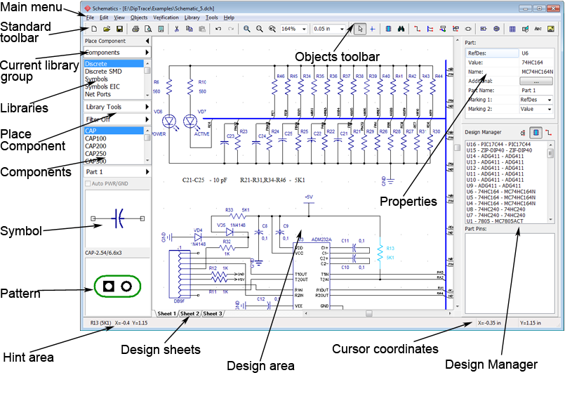
Design area – create and edit schematic objects (parts, wires, buses, shapes, tables, etc.). Access to all common functions of the program via the main menu.
Standard toolbar – tools to work with files, cut/copy/paste objects, print, preview and configure titles, change scale and grid size.
Objects toolbar – default mode, define origin, find and place components, create and edit wires and buses, place page connectors (Bus connectors), define differential pairs, place hierarchy connectors and blocks, place shapes, texts, and tables.
Place Component panel – displays all active libraries, user libraries or only components of the current project. Select library from the list, find component using the search filters and place it. Setup the panel, search filters, multi-part component placement tools, symbol and pattern previews. To adjust the panel width, right-click on it and select preferred option.
Properties panel – displays the properties of an active tool or selected object/s.
Design Manager – allows to quickly find any component or net in the circuit.
|
Press Press |
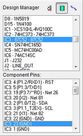
 button to see the list of components, or press
  button to see the list of nets. Select component or net in the list, and all pins of selected component or net will appear in the list right below. Left-click in the list to highlight an object or double click it to pan the design area to selected object.
Status Bar – shows the current hint, mode, grid status and the cursor coordinates.
See DipTrace Help for details ("Help / Schematic Help" from the main menu).
Go to "View / Toolbars / <toolbar>" to hide / show any of the UI toolbars (or use Ctrl+1 through 4 hotkeys).
3. Custom keyboard hotkeys
DipTrace features customizable hotkeys in all software modules. This makes switching to DipTrace especially convenient and fast since you can assign keyboard shortcuts that you've used to work with. Go to "Tools / Hotkey Settings" from the main menu in Schematic, however, the same main menu item leads to the Hotkey Settings dialog boxes in any of the DipTrace modules: Schematic, PCB Layout, Component and Pattern Editors.
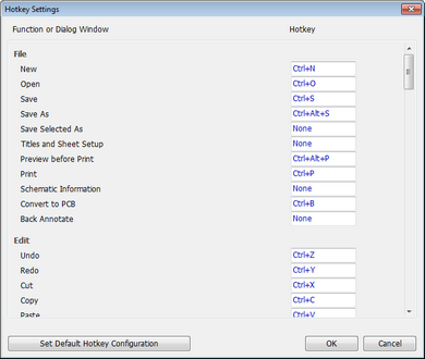
In our case, we have Schematic hotkeys, but described here can be applied to customizing shortcuts anywhere in DipTrace. In the Hotkey Settings dialog box, you can assign custom keyboard shortcuts to most DipTrace tools, program actions, and dialog boxes.
Let's assign another keyboard combination for creating a new file:
- Left-click in the corresponding field,
- Press key or key combination.
If the combination is already assigned to another tool you can either proceed with a new shortcut, or leave the old one.
Notice that all hotkeys mentioned in all topics of this tutorial are default ones.
Press Set Default Hotkey Configuration button to restore default values.
Notice that certain keys and combinations are reserved by the system. Please refer to the Hotkeys topic in the Schematic Help document ("Help / Schematic Help" from the main menu) for a complete list of reserved key combinations in DipTrace Schematic. Check out the corresponding topics in PCB Layout Help, Component Editor Help, and Pattern Editor Help to get more information about hotkeys in the respective programs.
4. Establishing schematic size and placing titles
We'll start with establishing the size of the schematic sheet and placing the drawing frame, go to "File/ Titles and Sheet Setup" from the main menu, and select ANSI A from the Sheet Template drop-down box. Then go to the bottom of the dialog and check Display Titles and Display Sheet items. Press OK.
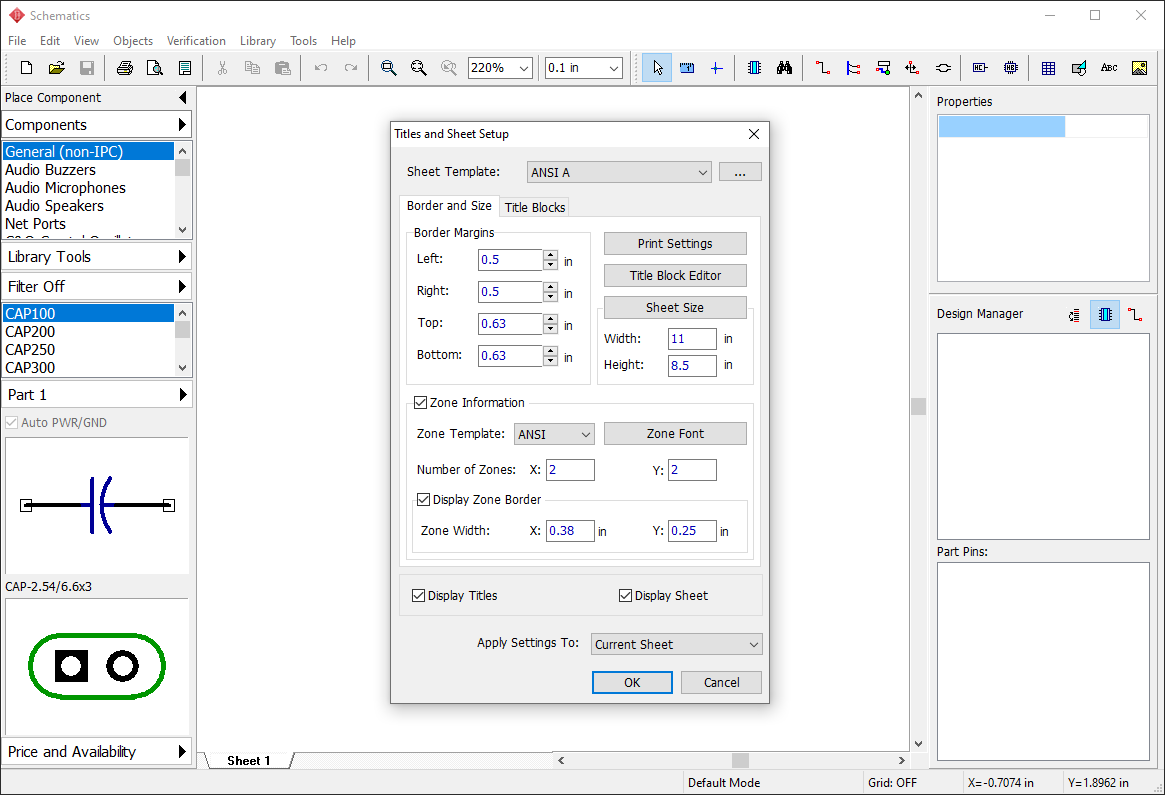
Notice that you can show/hide titles and sheet on the design area by selecting "View / Display Titles" and "View / Display Sheet" from the main menu.
Now press the Minus Sign (-) hotkey to zoom out until you can see the drawing frame. Plus and Minus signs (+) (-) hotkeys, the mouse wheel, and the scale box on the Instruments toolbar allow for zooming on the schematic. Hover over the required area for more precise zooming. Notice that you can hide the Design Manager panel on the right (Ctrl+2 hotkeys) to get more space on the design area.
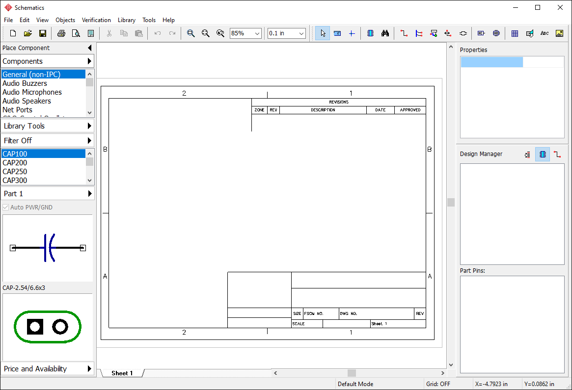
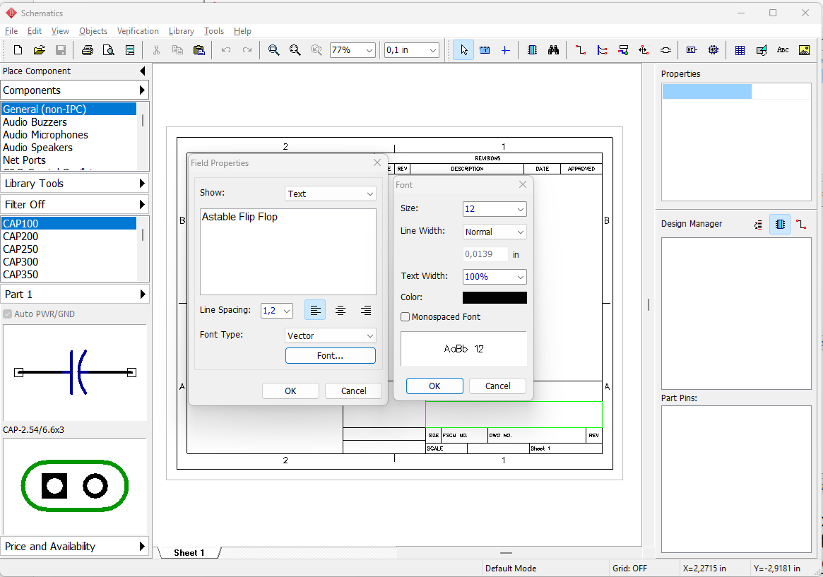
To enter text into the title field, simply hover over that field with the mouse (the field highlights green), then left-click it to open the field properties pop-up dialog box, select or type in the text (field content), define alignment (Left, Center or Right), and the font.
In our case type in "Astable Flip Flop" text, then press the Font button and set the font size to 12. Then click OK to close the dialog box and apply changes.
You can enter multi-line text into the title block fields. This text will be saved only for the current project. If you need to create a custom title template with predefined texts, please refer to Title Block Editor (more details in Schematic Help Title Block Editor topic).
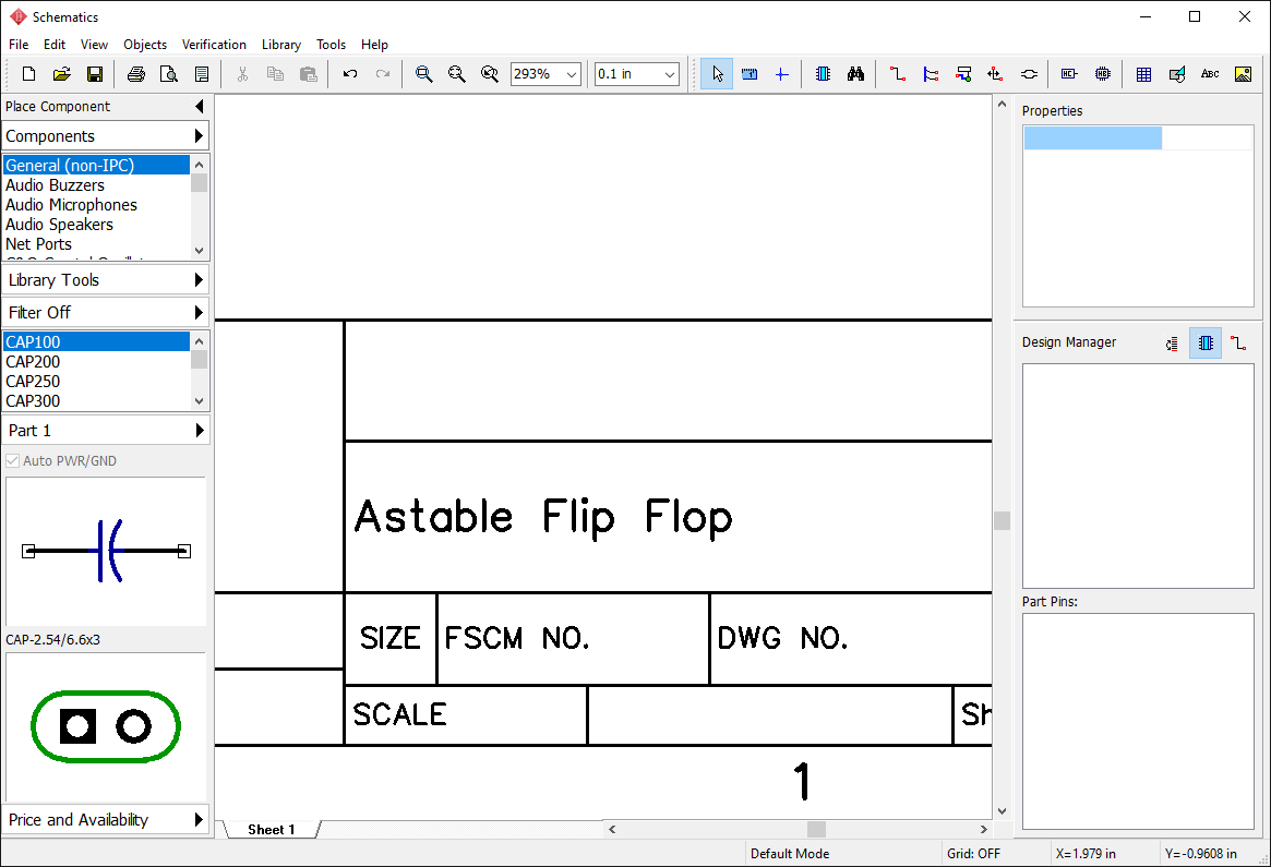
To zoom on the title block, hover over it with the mouse, and press the Plus Sign (+) or scroll the mouse wheel.
Let's practice with different zoom options for a while. Click on the  button (Zoom Window) and draw a rectangle on the design area where you want to zoom.
To return to previous scale and position, use  button (Undo Scale). Press and hold the right mouse button to pan on the design area.
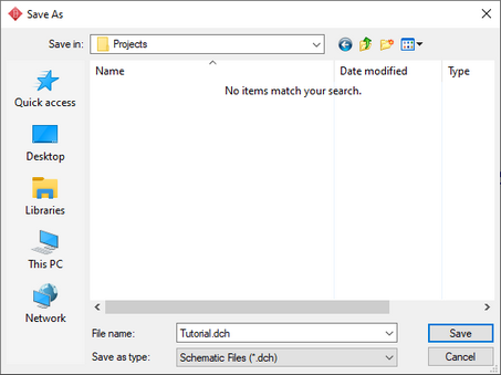
Go to "File / Save As" from the main menu, type in the file name, and make sure that file is in the directory that you need. Select the file type — binary or XML. The XML format is recommended for version control. Click Save.
5. Configuring libraries
|
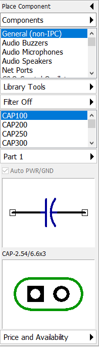
DipTrace has a single cross-module library management system. Libraries are organized to standard and custom library groups with multi-level search filters ensuring that correct components can be found quickly. The Place Component panel has all necessary tools to place components and manage libraries. To adjust the panel width, right-click on it and select preferred option or just hover over the panel border and drag it.
Configuring library groups Press Components (all standard libraries, sorted alphabetically by component type and manufacturer); User Components (add/delete libraries to/from this library group). Empty by default; Project Libraries (auto-generated library with all components of the current circuit). It is empty if no schematic file is open.
Let's group all libraries that we will need for our project into a single library group. Select User Components library group, then press the |

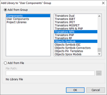
Now the selected libraries have appeared in the User Components library group and we are ready to start designing the schematic.
Add library from a separate file
To add a new library to the DipTrace library system, check Add from File checkbox in the Add Library to <Library group> dialog box and select the file on your computer. You can also use the Library Setup dialog box to get access to the comprehensive library system settings ("User Components (<Current library group>) / Library Setup" on the Place Component panel).
Notice that Library Setup panel allows for configuring both pattern and component library groups, though pattern libraries are invisible in the Schematic.
More information in the DipTrace Help ("Help/ Schematic Help" from the main menu), Working with Libraries section.
6. Designing schematic
In this section of the tutorial we will show the basic principles of working in the Schematic module of DipTrace PCB Design Environment.
Please turn ON the grid (if it was turned OFF) with F11 hotkey. Change the grid size to 0.1 inch, you can select it from the drop-down list of grids on the Instruments toolbar, or press the Ctrl + Plus Sign (+) hotkeys to increase, or Ctrl + Minus Sign (-) to decrease the grid size.
Notice that you can add new sizes by selecting "View / Customize Grid" from the main menu. Precision of grid and all values used in the project can be defined in View/ Precision dialog. Measurement units can be changed in the "View/ Units" main menu item or with Shift+U shortcut. We will use only default keyboard shortcuts in this tutorial. Go to "Tools/ HotKey Settings" to restore the defaults or change shortcuts.
Now let's start creating the circuit. Select Transistors NPN library from the User Components library group on the Place Component panel.
Search component in libraries
|
Once the library is selected, scroll down the component list to find 2N2221AL transistor or use the search filters. Select "Objects/ Find Component" from the main menu or press In the pop-up dialog box make sure that Transistors NPN library is set as a search area, then type in "2N2221AL" into the Keywords field, and press Apply Filter. Now only components containing 2N2221AL appear in the component list. The filters button now shows that the filter is ON. All other components are hidden. |
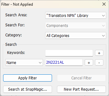

Close the Search Filters dialog box.
Notice that you can expand the search results by entering a part of the component name as well as filter components by RefDes, value, pattern, manufacturer, datasheet, or additional fields, use the  and
and  buttons to add or delete the search filters.
Placing components
Click on the transistor in the list and move your mouse pointer to the design area. Left-click once to place one transistor. Right-click to disable the component placement mode.
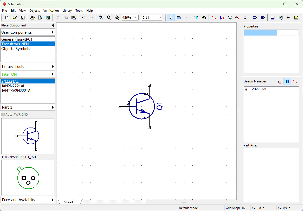
Drag and drop component if you need to move it to another location on the design area.
To select several objects, press and hold the Ctrl key, then left-click on each object that you want to add to the selection or move the mouse to the upper-left corner of the group, hold down the left mouse button and move cursor to the lower-right corner, then release the mouse button to select all objects inside the rectangle (press Ctrl key to invert selection). Now you can move all these objects at a time.
Sometimes it is necessary to change the reference designator of the component. Hover over the component with the mouse pointer, right-click it, and select the top item (Q1) from the submenu. In the pop-up dialog box type in a new RefDes if needed. We will keep "Q1".
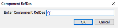
We need two transistors for the schematic, select 2N2221AL in the component list again, and place it on the design area. If you have changed the reference designator you don’t need to rename the second transistor, it happens automatically. If you want to rotate the component before placing it on the design area, press Space or R default keyboard shortcuts.
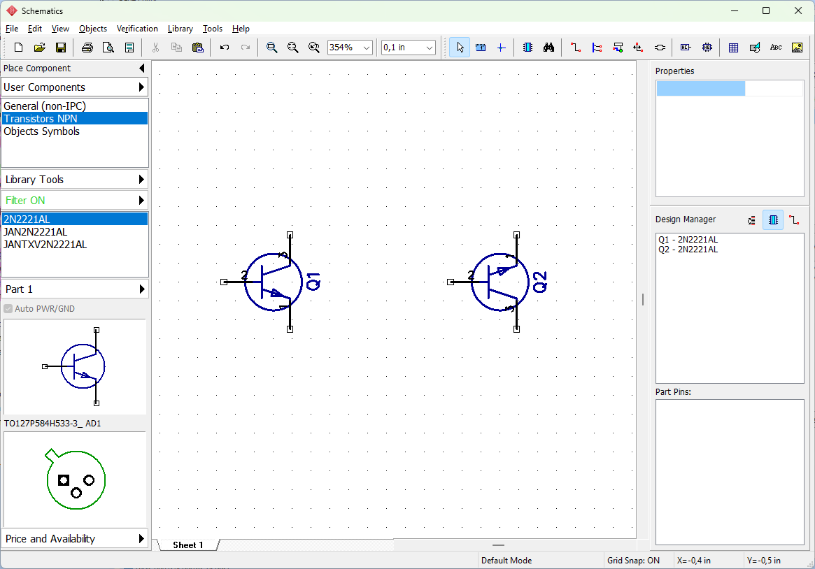
You can activate Snap to Grid option, if it's disabled (View/ Snap to Grid or Alt + F11), this will align the newly placed components by the grid. Grid Snap status is displayed on the status bar in the bottommost part of the screen.
When the search filter is active, you can see only certain (filtered) components of the library. Press Filter ON button on the Place Component panel, then press Cancel Filter in the pop-up dialog box to turn the filtering OFF. Now close the search filters dialog box.
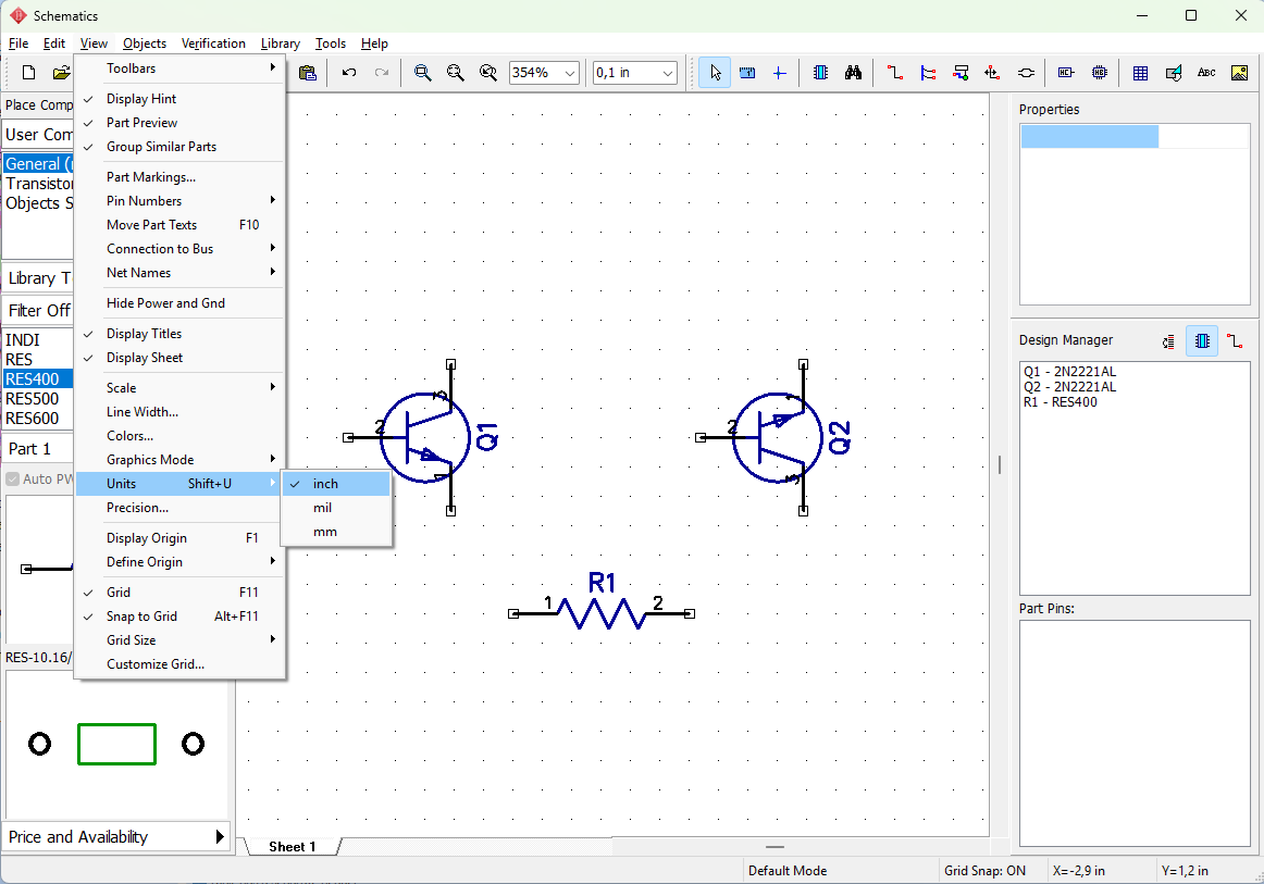
Select General (non-IPC) library, find RES400 resistor, and place it on the design area. If you prefer metric units, switch units with Shift+U combination or select the Units in View submenu, however, we will keep inches as these are the most suitable units for the current project.
Copy components
We need 4 resistors for this project. You can place them manually, like Q1 and Q2 transistors, but this time we select one resistor on the design area and copy it three times. There are two ways to copy a component:
1. Once a component is selected, go to "Edit/ Copy" from the main menu or right-click on the component, and select Copy from the submenu (Ctrl+C hotkeys), then select "Edit/ Paste" three times, or right-click on the design area, and select Paste (Ctrl+V hotkeys) from the submenu.
2. Copy Matrix. This option is good for bulk copying. Select resistor, then go to "Edit/ Copy Matrix" from the main menu (or press Ctrl+M hotkeys).
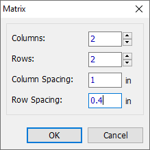
In the Matrix dialog box set the number of columns and rows ("2" columns and "2" rows to get 4 resistors) and spacing (1 inch for columns and 0.4 inch for rows is good), click OK. Now you can see four resistors on the design area:
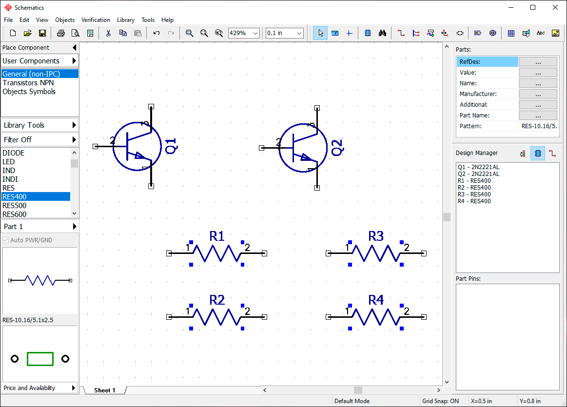
Move resistors to a proper location, like in the picture below (use mouse or arrows on the keyboard for orthogonal moving), and rotate components 90 degrees (use Space or R shortcuts to rotate selected components). Another method to rotate an object is by using the "Edit / Rotate" main menu item or right-clicking on the object and selecting Rotate from the submenu.
Notice that you can pan design with the right mouse button or the mouse wheel: move mouse arrow to the design area, hold down the right mouse button or the mouse wheel, and pan.
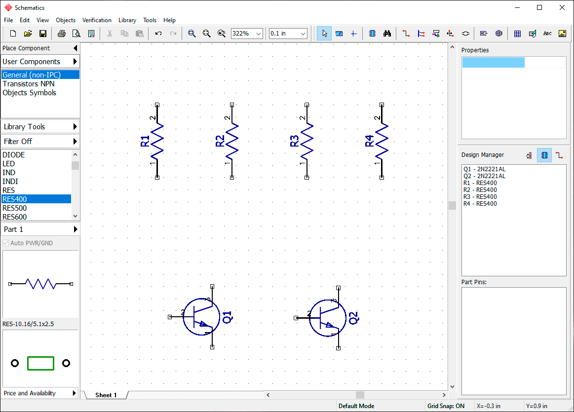
Components' markings
The reference designators of Q1 and Q2 transistors have inappropriate locations, we need their RefDes to be under the component symbols. To change the RefDes location, select both transistors, right-click on one of them, and select Properties from the submenu. In the pop-up dialog box open Part Markings tab, and select Bottom from the Align drop-down for RefDes.
Let's display component names for these transistors too. To do that, in Name line select Show from Show drop-down and Corner from Align drop-down. This will show the names of selected components. Notice that reference designators are already displayed as primary markings. Common means using common Schematic settings for all components (defined in View/ Component Markings).
If you want to set precise position of a marking, select Position from the Align drop-down - Position column will become active, press  button to set X and Y coordinates and rotation angle for the corresponding Markings.
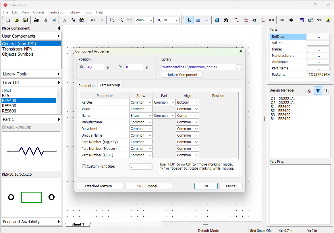
Press OK.
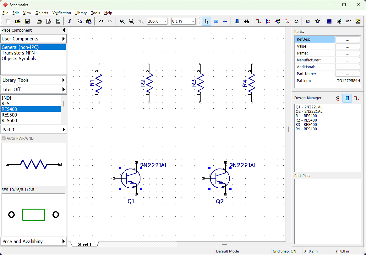
You can show or hide pin numbers for the entire circuit by selecting "View / Pin Numbers / Show" from the main menu, if they are not displayed yet. To change pin display settings for the selected part, right-click it, and select Pin Numbers from the submenu.
However, if you're still not satisfied with location of RefDes, numbers, pin names or any other markings, you can move them around visually with a special move tool. Select "View/ Move Part Texts" from the main menu or press F10. For precise moving it's better to disable Snap to Grid option (Alt +F11 hotkey). You can move and rotate part markings like separate objects with R or "Space" shortcuts.
"View/ Part Markings" menu item allows the user to change common settings of part markings. Common settings are applied to all schematic parts, except those with custom properties.
Use Undo or Redo tools ( buttons) if you are not satisfied with the changes you've made. The DipTrace saves up to 50 steps. Remember to save schematic into a file. Select "File / Save" from the main menu or press the Save button on the Standard toolbar. If the current schematic has never been saved, the Save As dialog box will pop up to define the file name and location. If the file already exists, clicking the Save button or pressing Ctrl+S hotkeys is enough. You can use the "File/ Save As" dialog box to save the same file under a different name, for example, in order to backup it. The XML file format can be used for version control.
Create connections
Connect pin 1 of R1 resistor to pin 2 (base) of transistor Q1. You need to make sure that you are in the default mode ( button is pressed). Hover with the mouse arrow over the bottom pin of R1 resistor, and left-click it - Place Wire mode will be activated automatically. Then move the mouse arrow down to the base pin of the Q1 transistor, and left-click it to connect the wire and create the connection between R1 and Q1. Place Wire mode can also be activated using the toolbar button
  or from the main menu: Objects / Circuit / Place Wire.
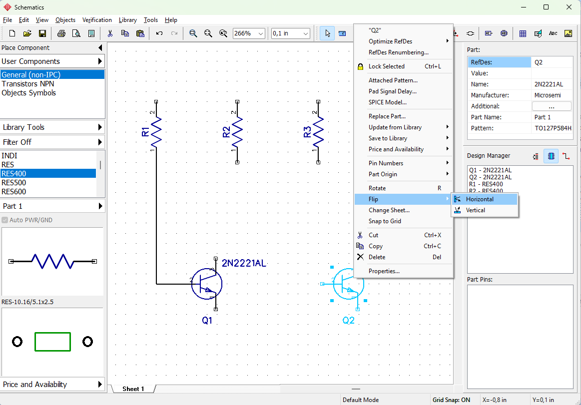
Now we need to mirror the Q2 transistor, this will make schematic easier to understand. First, return to the default mode by right-clicking on a empty spot, then right-click on the transistor, and select "Flip/ Horizontal" from the submenu.
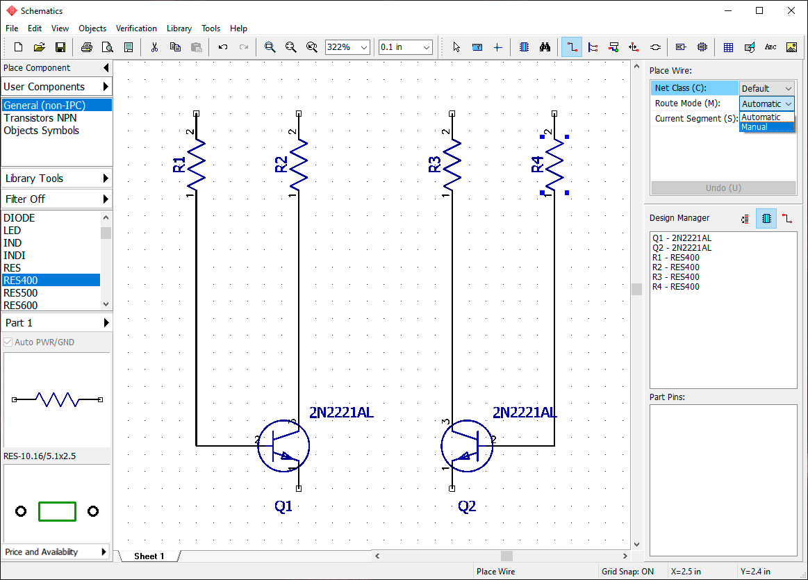
Connect R4 to pin 2 (base) of Q2, R2 to pin 3 of Q1, and R3 to pin 3 of Q2, like in the picture below. You can move components or wires to get straight lines, this is not important for electrical connectivity, but necessary to make schematic well-organized and easy to understand. If you don't like the automatic wire placement mode, you can turn it OFF on the Place Wire panel of the Design Manager to your right-hand side. Set Manual in the Route Mode section or just press the M hotkey. Place Wire panel is only visible in the wire placement mode.
Now select CAP100RP from the General (non-IPC) library and place it twice to the design.
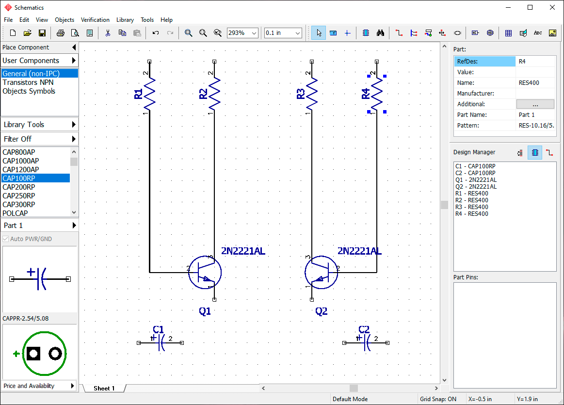
Flip C2 capacitor, select "Flip/ Horizontal" from the right-click submenu. C2 capacitor's positive pin should be facing right.
We need to place two capacitors between the transistors Q1 and Q2 with respect to their polarities.
You might need to move some components to give enough space for the capacitors and connections.
Move resistors a bit upwards, and select Q2, R3, R4 and related wires in order to move them to the right a little bit. Draw a selection box around these objects by holding down the left mouse button.
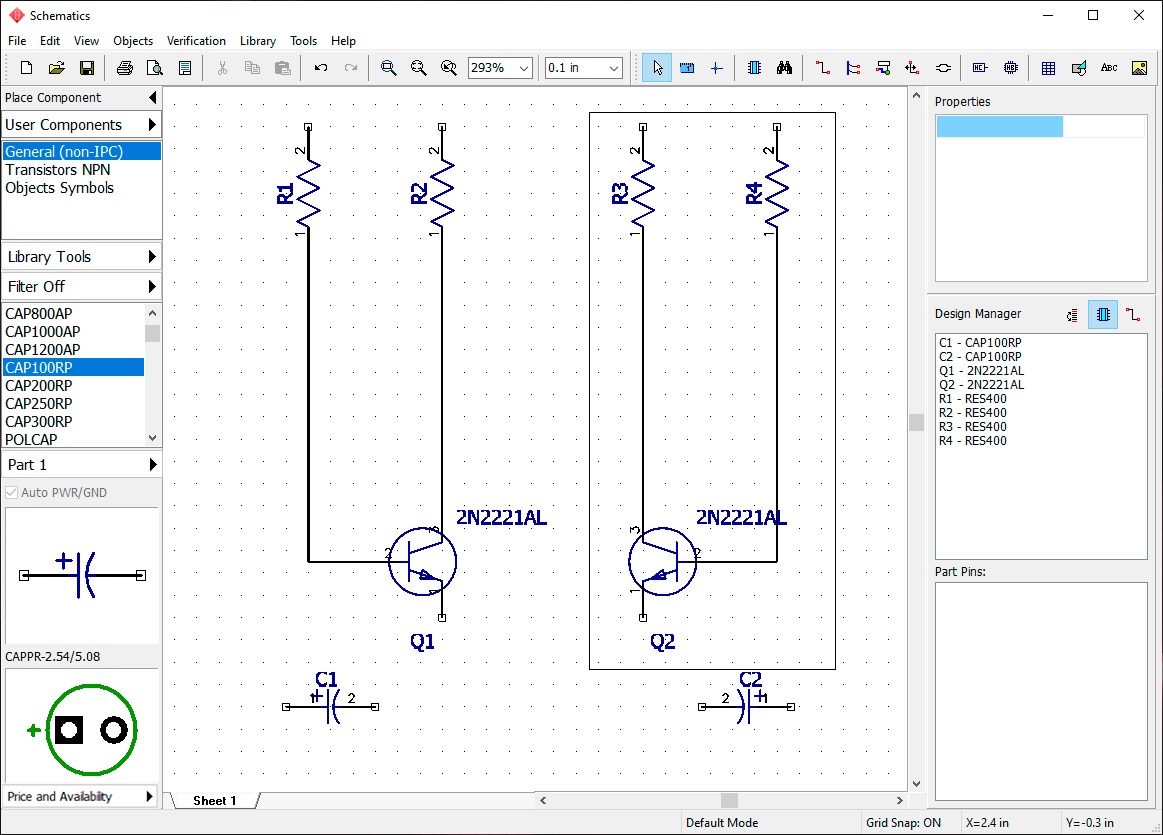
Right-click to deselect all, if you are in the Default mode, or double right-click if you are in another mode (first click to disable an active mode and the second click to deselect all).
Connect the positive pin of the C1 to pin 2 of the Q1: left-click the C1 positive pin and left-click on the wire between the R1 and Q1, the small circle appears if wires are properly connected.
Then connect C1 pin 2 and C2 pins like in the picture below.
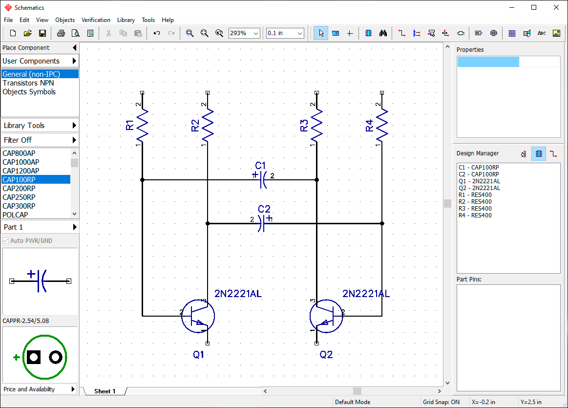
Scroll down the components list of General (non-IPC) library on the Place Component panel to find LED component, and place two of them onto the schematic. Then change the reference designators to "LED1" and "LED2" (right-click on the component, and select the first item from the submenu), rotate these parts with R hotkey or Space (pressed three times). Probably, you'll need to move and rotate the RefDes with the Move Part Texts tool (F10 shortcut). Then connect LEDs to transistors like in the picture below.
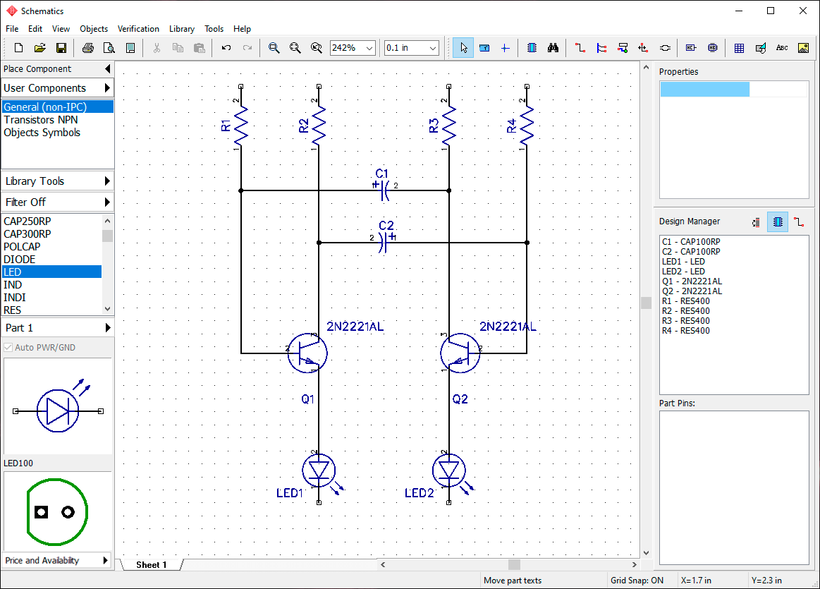
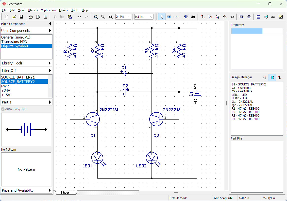
Place a battery symbol SOURCE_BATTERY2 component from the Objects Symbols, change its RefDes if you need, and complete the circuit by connecting the remaining pins (see the picture). Make sure that you see small black circles where two wires connect, if not, then wires are not connected.
Notice that you can align components in rows or columns automatically respective to each other, just select the components that you want to align, right-click on one of them, select Align Objects from the submenu, and set up the alignment tool properly. However, it's not needed for the current schematic.
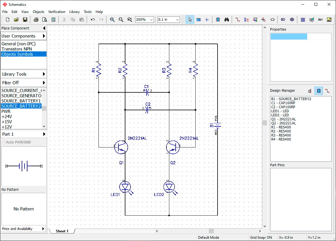
If you want to move existing wire, hover over it with your mouse (the net should highlight and the mouse cursor shows possible directions), then left-click on the wire and move it while holding the left mouse button.
Notice that if you are in the Place Wire mode and you click on the existing wire, you start creating a new wire, not editing an existing one. The Place Wire mode is enabled automatically when you left-click on any component pin.
If some objects do not highlight when you hover over them with the mouse, right-click on any free spot on the design area to switch to the Default mode. If you want to delete a wire, right-click it to open the submenu, and select Delete Wire. To delete a wire segment, select Delete Line from the same submenu. You can use the Undo to return to the previous state of the circuit.
Now we will add resistance values "10kΩ" for all resistors on this schematic. Vector fonts in DipTrace support Unicode characters, so switching to TrueType fonts is not required. However, you can still use TrueType fonts for part markings if needed. To do this, go to "View / Part Markings" and select a TrueType font in the pop-up dialog box. We will keep the Vector font. If necessary, it can be set to monospaced by enabling the "Monospaced Font" option in the settings.
Notice that there are various ways to enter special characters. We recommend to copy symbols from the Character Map ("Start / All Programs / Accessories / System Tools / Character Map" in Windows OS), and paste them in the DipTrace.
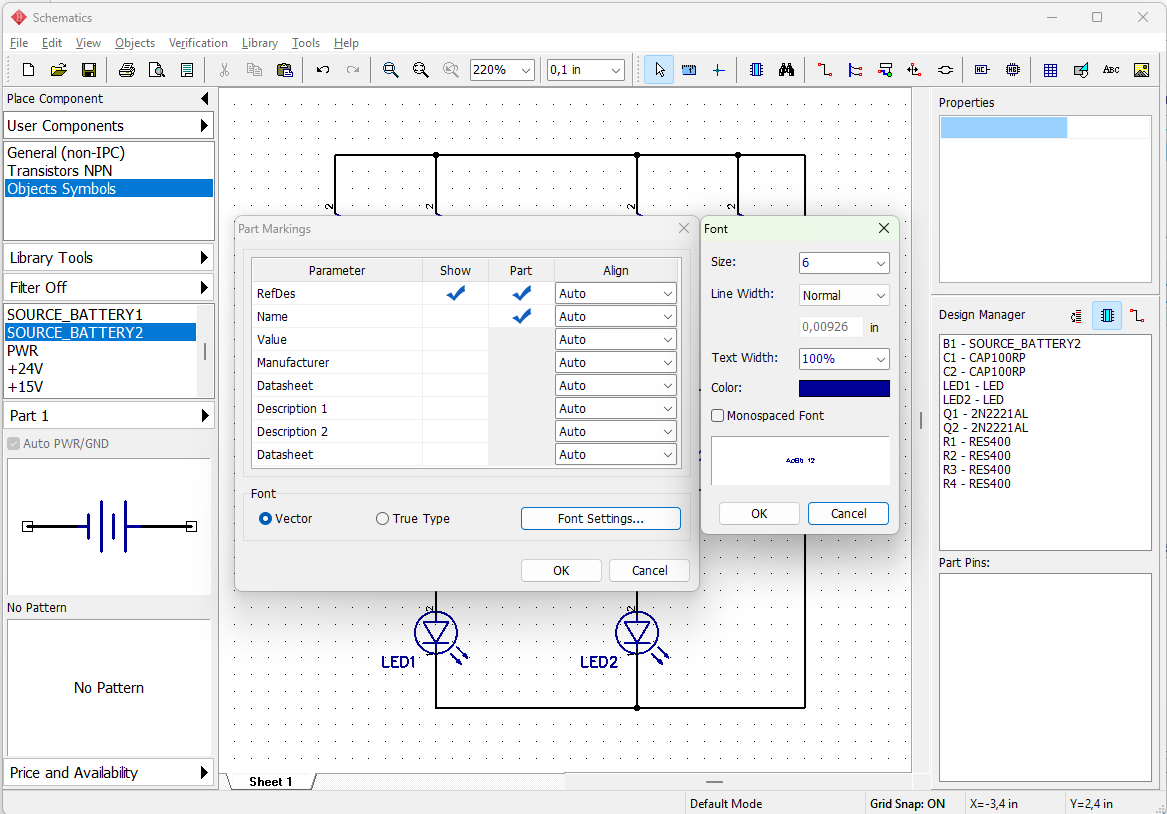
Now select all resistors, then right-click on one of them, and select Properties from the submenu. In the Parameters tab type "47 kΩ" into the Value field. Now open Part Markings tab. In Show column select Show from the drop-down for Value, click OK.
As you remember, we took the battery component from the Objects Symbols library. All components in this library don't have patterns, they are just symbols (pattern preview field on the Place Component panel says "No Pattern"). But in order to proceed to the PCB layout stage, you should attach the related pattern to this symbol. If left blank, DipTrace will not be able to show this component on the circuit board and an error dialog box will pop up.
Hover over the battery symbol, right-click it, and select Attached Pattern from the submenu. In the pop-up dialog box you can see the list of all components of the current circuit in the left part of the dialog box, make sure "B1-SOURCE_BATTERY2" is selected (you can see the battery symbol in the preview field).
Select Patterns library group from the Pattern Libraries drop-down list on the right. This library group contains all standard DipTrace pattern libraries separately from the symbols. Select Batteries library from the list and find PANASONIC_BR-1225_VCN pattern in the pattern list at the bottom-right of the dialog box (use the search filters if you want). In most cases, DipTrace automatically assigns pin-to-pad connections according to the pad numbers, but this is not the case with this battery symbol.
Positive pad is usually square shaped and negative is round. Click on the corresponding row in the Pin to Pad Table, and type in related pad number in the Pad Number column (NEG pin should refer to Pad #2, POS pin – to Pad #1). Pattern pad numbers can be displayed by enabling the "Show Pad Numbers" option in the "Check Pattern Dimensions" dialog.
You can visually set pin to pad connections, just left-click on the pin in the symbol preview field, and then on the corresponding pad in the pattern preview field.
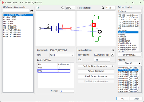
Press OK when ready to close the Attach Pattern dialog box.
Notice that some symbols in the libraries are intentionally made without attached patterns (for example, VCC, GND or other logical connectors, Net Ports).
Our schematic is now ready to become a PCB. Do not forget to save the schematic, select "File / Save" from the main menu or click on the Save button or simply Ctrl+S.
You can print schematic or save it in BMP or JPG file. You can also export it to PDF.
Select "File / Preview" from the main menu, in the pop-up dialog box customize the preview, and press Print All to print all schematic sheets, or press Print Current Sheet to print the selected sheet, press Save to create a BMP/JPG/PNG file with defined resolution. To export the schematic to PDF, press Export PDF.
7. Converting to PCB
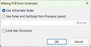
You can open DipTrace schematic files (*.dch) in PCB Layout module, but if you want to save your time, select "File / Convert to PCB" or press Ctrl+B hotkeys directly in the Schematic. In the pop-up dialog box you can use Schematic rules or load rules from any other PCB layout file. When you press OK, the schematic will open in the PCB Layout.
|
In case of incorrect exit from the program or if you somehow forgot to save the project, it is possible to recover the latest schematic by selecting "File / Recover Schematic" in the Schematic or "File / Recover Board" in the PCB Layout module. |
If you want to hide the Design Manager to get more space on the design area, press Ctrl+2 hotkeys or uncheck "View /Toolbars / Design Manager" main menu item.
Designing a PCB
8. PCB Layout UI
DipTrace PCB Layout's main window includes the design area, the main menu, toolbars, the Place Component panel, Design Manager with layers/objects/properties panel, and the status bar.
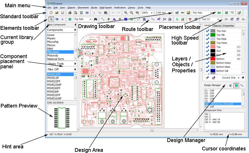
You can place and edit different objects (components, ratlines, traces, copper pours, shapes, tables etc.) on the design area. The main menu provides access to all common features.
Other interface elements:
Standard Toolbar – tools to work with files, cut/copy/paste objects, print, preview and configure titles, launch 3D Preview, change scale and grid size.
Elements Toolbar – tools to switch to the default mode, measure, change origin, place components, ratlines, pads, vias, mounting holes, copper pours, dimensions, and tables.
Route Toolbar – tools to create and edit traces, create a board outline, run and setup the autorouter, check design rules, select current signal layer.
Placement Toolbar – placement and auto-placement tools.
Drawing Toolbar – tools to create shapes, text, insert images, and select shape and text placement layer.
High Speed Toolbar – define differential pair, edit single trace of a differential pair, free single trace editing mode, add meander, and phase tune tool.
Place Component panel – select library, select component and place it on the design area. Library groups, library tools, search filters, pattern preview.
Layers / Objects / Properties panel (active tab depends on current selected object/tool/mode).
The Layers tab allows for working with layers (show/hide, add/delete/edit, change position and layer color) and changing layer display mode;
The Objects tab allows the user to show/hide different objects on the design area and block certain objects from being selected;
The Properties tab shows properties of selected tool/object and allows the user to change them.
Design Manager – allows to quickly find any component or net in the circuit board, the same as in the Schematic.
|
Press Press
|
Status bar – shows the standard or detailed pop-up hint (containing pad/via/hole dimensions, trace length) for the objects on the design area, the current mode (Default, Route Manual, Edit Traces, etc.), view (Normal, Mirror, the current Snap to Grid, and coordinates of the current position of the cursor or selected element.
Go to "View / Toolbars / ..." to hide/show any of the UI toolbars (or use Ctrl+1 through 9 hotkeys). See DipTrace Help for details ("Help / PCB Layout Help" from the main menu).
Routing: preparation, layers and vias
9. Preparing to route
The routing itself is one of the final stages of board design, but its quality greatly depends on the preparation.
Right after converting to the PCB, the circuit looks chaotic. Press  button on the Placement toolbar or select "Placement / Arrange Components" from the main menu, all components will be placed near the design center, called the Origin (blue line cross), and arranged according to the placement settings. If the Origin is not displayed, you can enable it using the F1 hotkey.
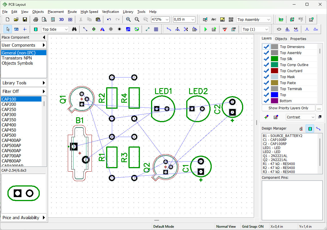
You can use Auto-placement or Placement by list features after converting to PCB. These are very convenient and useful tools which allow the user to get advantages of both automatic and manual placement modes. We will place components automatically in Part III of this tutorial with more complex circuits.
Component markings
Make sure that reference designators are visible. Select "View / Component Markings" from the main menu. In the pop-up you can set up display parameters for reference and other designators of all components of the current project, except those with individual settings, in the Silk Screen and/ or Assembly Layers. In Show column tick the parameters you want to be shown; we'll select only RefDes. You can leave Auto alignment mode and let DipTrace select the best alignment option for markings or select another mode (Center, Top, Bottom, Left, Right, Corner). Uncheck Rotate Markings with Component if you want marking to maintain its position when a component is rotated.
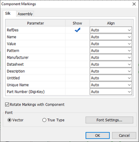
For the PCB Layout we recommend vector font in most cases. The vector font can be configured as monospaced.
To change the font parameters of the marking text, press Font Settings button. You can choose any size, but don't make it too big (we'll set 5 pt).
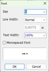
To define custom component marking parameters for the selected components, right-click on one of them, select Properties from the submenu, then select the Markings tab in the pop-up dialog box. You'll be able to define, which Markings to show, how to align them as well as their position, rotation angle and font size for both Silk Screen and Assembly layers.
Remember that you can use the move tool – F10 or "View / Move Component Texts". This option allows for moving and rotating (90 degree step) any text object on the board.
Manual placement
Now distribute the components manually, according to your preferences and design rules. It is a good practice to keep power supply components in one area and functional blocks in another. Apply appropriate layout rules and differential signaling for high frequency circuits. Notice that we use 0.05 inch (1.27 mm) grid; you can change it using a drop-down list on the Instruments toolbar. Grid display can be toggled with the F11 hotkey, and grid snapping can be enabled with the Alt+F11 hotkey. Select "View / Units / Inch" main menu item to change the measurement units or press Shift+U. You can configure precision of all the values used in the current project as well as set grid minimum size and precision. To do that, open a dialogue-box by selecting Precision item in View submenu.
Create a layout similar to the one in the picture below, with resistors at the top and LEDs at the bottom of the board. Drag and drop components to move them on the board. Press Space or R default hotkeys to rotate selected components by 90 degrees. If you need to rotate by a different angle, select components, then right-click on one of them, and choose Define Angle or Free Rotate for precise and visual rotation respectively.
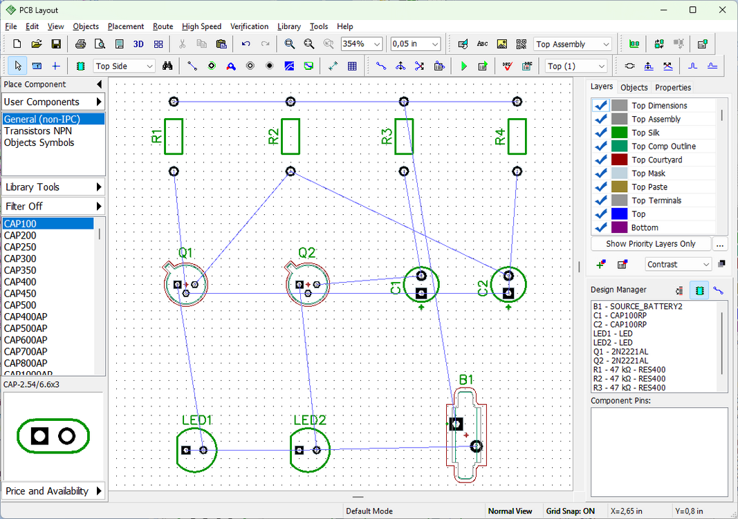
Aligning objects
|
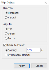
This project is simple and guidelines that appear while moving components will help you align them, but you can also use the Align Objects tool to organize components in rows and columns automatically. For example, select four resistors (use the box selection or the Ctrl key to select multiple objects at a time), then right-click on one of them, and select Align Objects from the submenu. In the pop-up dialog box, set Horizontal direction, check the Distribute Equally and Spacing checkboxes and enter 0.55 inch in the Spacing field. The Align By section of this dialog box does not matter to us because we are aligning similar footprints. Press Apply. Press F12 to optimize visual appearance of the connection lines on the screen (this does not change the net structure). |
Changing the net structure
We're going to practice in changing the net structure on the board, adding and removing connections. Blue thin lines between pads show logic connections, these lines are called "ratlines".
Hover over any pad with the mouse, right-click it, and select Delete from Net, the pad will disappear from the net. This pad is no longer connected with a blue line.
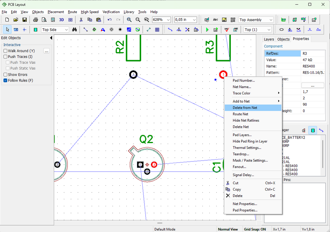
You can create a pad-to-pad connections visually. Select "Objects / Place Ratline" from main menu or press  button on the objects toolbar. Then hover the mouse pointer over unconnected pad, left-click it, and move your mouse to any other pad (connected or unconnected), and left-click it. A new wire or a new net (in case if both pads were unconnected), represented as a thin blue line (ratline) will appear. To delete an existing connection, just select Delete Net from the right-click submenu on the pad.
If you would like to add a pad to some net without creating a connection visually on the design area, hover over the pad with the mouse, right-click it, and select Add to Net/ Select from List, then select net from the list of all nets of the project or select the option Add to Net/ Select by Mouse Pointer to point the required net with the mouse cursor on the design area.
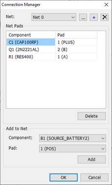
However, the most convenient way to add, delete or rename nets, as well as add or delete pads to/from the nets is the Connection Manager. Select "Route / Connection Manager" from the main menu to launch it. Connection manager is easy to use.
|
Select a net from the Net drop-down list and you will see all pads of the net in the table; you can easily delete any one of them. If you want to connect some pad to the net, select a component and its pad, using the drop-down menus at the bottom of the dialog box, and press Add button. If you have changed the net structure, please press Undo until previous design is restored. Close the Connection Manager. By the way, if you lose design or schematic because of incorrect exit from the program, use "File / Recover Board" in the PCB Layout and "File / Recover Schematic" in the Schematic to recover the latest project version. To protect the net structure from accidental change, select "Route / Lock Net Structure" in the main menu. |
Board outline
We haven’t determined the board outline yet. If you launch the autorouter, it will create an appropriate rectangle board automatically, but in real life electronic designer usually has certain board requirements well before starting the project. You can create a relatively simple board polygon directly in the DipTrace or import it from the DXF file (if its shape is complex).
Select "Objects / Place Board Outline" or press  button on the Routing toolbar, then place the board outline by left clicking the key points on the design area. Right-click in the final point of the polygon, and select Enter from the submenu or press Enter on the keyboard. For this design we require a simple rectangle board about 2.5 x 2.5 inches, see the picture below (notice that the origin point is hidden with F1 hotkey).
If necessary, you can create arcs in the board outline by selecting Arc from the right-click submenu while drawing the polygon. You can also select the most convenient Arc Mode (Start-Center-Angle; Start-End-Radius; Start-End-Middle Point) to build the arc from the submenu.
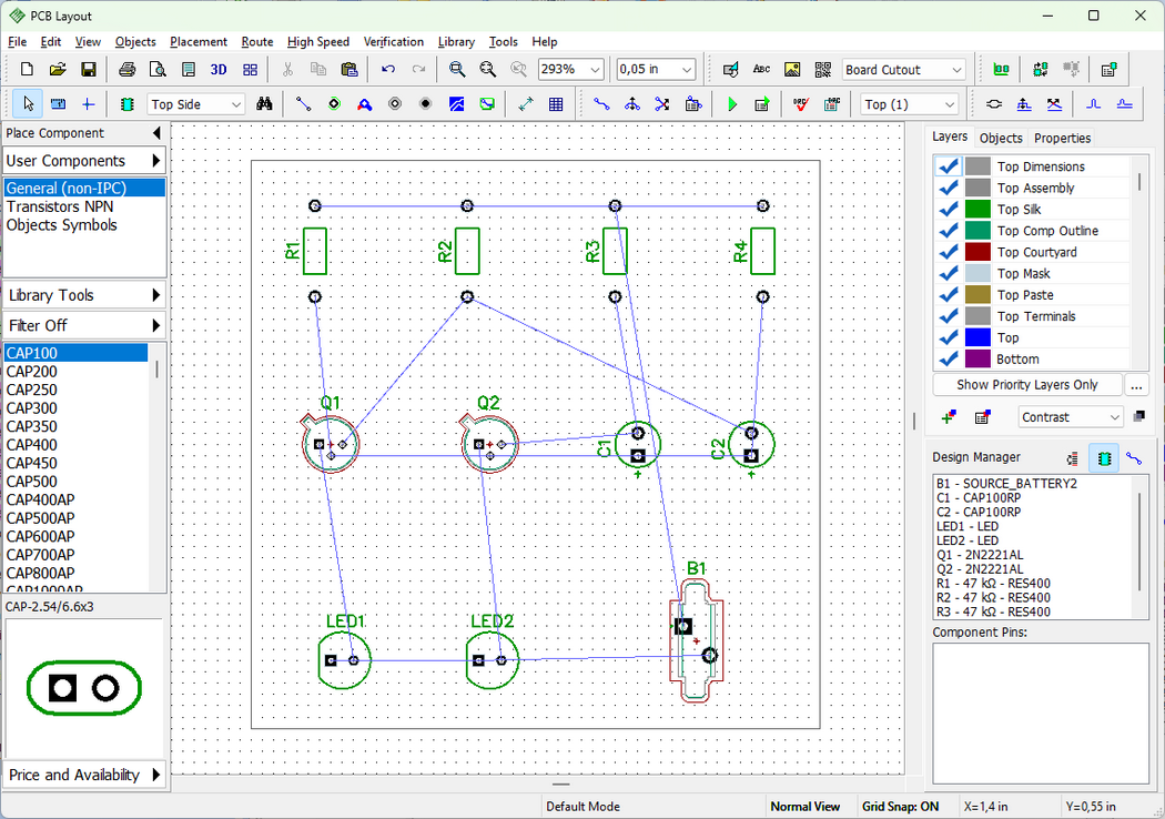
You can insert new points (right-click/ Insert Point) into the completed board outline polygon or move each point/ entire polygon on the design area. Point coordinates appear as a hint when the cursor hovers over it.
Another way to draw a board outline is to place a shape or a series of shapes (lines, polylines, arcs) so that they form a continuous contour in the Board Cutout layer (it should be selected from a drop-down on the Drawing toolbar), then right-click on the shape and select Convert to Board Outline.
There is one more way to create a board polygon that does not involve drawing it on the design area. Select "Objects / Board Points" from the main menu.
|
In this dialog box you can Add, Insert and Delete key points. Coordinates are shown and can be edited in absolute or incremental mode. If you check the Arc checkbox for some point, that point will become a middle point of an arc and the neighboring points will become the arc's first and end points. For rectangular boards, check Create Rectangular Board box and simply define the first point (base), width and height of the board. |
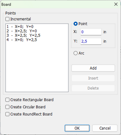
It is also possible to make circular and rectangular boards with rounded corners automatically.
Press OK to apply changes or Cancel to close the dialog box.
You can use "Objects / Delete Board" from the main menu, if you want to delete the outline polygon.
Origin point
Correct board origin is important, because it is the reference point and beginning of the coordinates for the circuit board. Bottom-left corner of the board outline is the best place. If you strictly followed the instructions given before in this tutorial, then you should see two blue lines crossing exactly there. However, in the case you do not see the origin point or it is not in the bottom-left corner of the board, select "View / Origin" from the main menu or press F1 hotkey to show it. If the position is wrong, go to "View / Define Origin / By Mouse Pointer" from the main menu or press  button on the Instruments toolbar, and left-click on the design area (DipTrace helps to target on the key points).
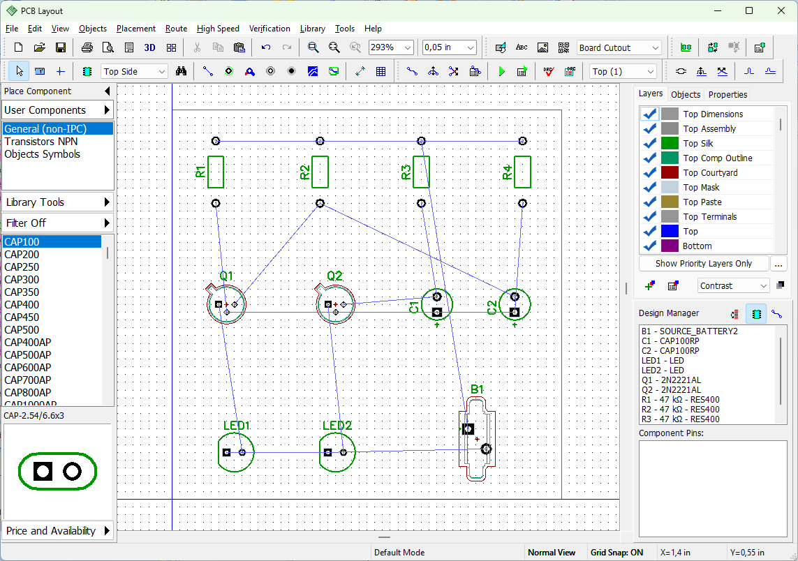
Now all coordinates in the PCB Layout will be displayed and edited relatively to the origin but you can change the origin's position at any moment.
Notice that coordinates of components on the board are calculated by pattern's origin point. It is defined in the Pattern Editor. To show or hide an origin of the selected component/s or to change its display mode, right-click on one of them, and select Pattern Origin from the submenu.
Board cutout
DipTrace allows the designer to create board cutout polygons. You can create a cutout of any shape but in our case, we will make a simple rectangle cutout between LEDs and transistors just to show you how to do this.
|
Select Board Cutout layer in the drop-down list on the drawing toolbar, then choose the rectangle drawing tool, and draw a rectangle cutout on the board on the design area. Pan, zoom and change the grid size for precise drawing. Board cutout is now ready. |
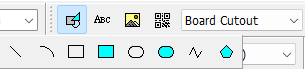
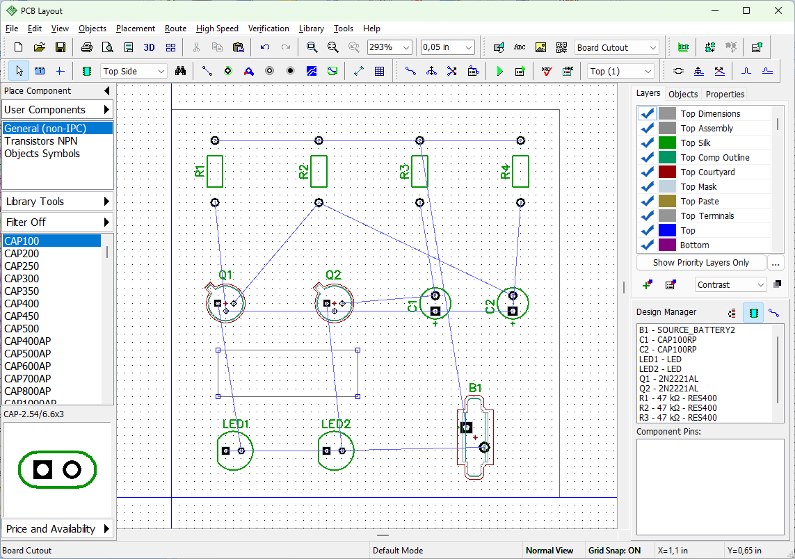
There is another way to create cutouts. Just draw a shape on any layer of the board or import it from the DXF file, then right-click on the shape, and select Properties from the submenu. In the pop-up dialog box, select Board Cutout from the Type drop-down list, and press OK.
Notice that board cutout does not visually differ from the board outline, you should be careful not to place a cutout instead of an outline.
Route Keepout
Route keepout is an area on the board not intended for any copper. Autorouter does not draw traces there, and the program will report errors, if you draw them manually in the keepout area. Board cutout shape does not have a clearance parameter like the board outline.
|
The route keepout around the board cutout will do the job. This allows for the clearance between the copper and the cutout. Since we plan to have copper traces only on the bottom layer, switch to Bottom layer with 2 hotkey, then select Route Keepout layer in the drop-down list on the Drawing toolbar, and select the Rectangle tool. Draw a rectangle which is a bit bigger than the cutout, like in the picture on the left. Change the grid size to 0.025 in for comfortable drawing. Then switch back to the top layer (press 1 hotkey). |
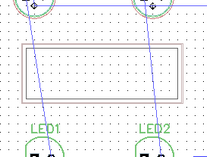
10. Autorouting
Now it is time to route the printed circuit board. DipTrace has a high-quality shape-based autorouter and the Grid Router suitable for simple PCBs and single-layer boards with jumper wires. Our project can be routed on a single layer (usually it is the bottom one). Single-layer boards usually have longer traces, but give many other benefits for prototyping. Longer traces do not affect the project this simple.
Select "Route / Current Autorouter" from the main menu, and choose Shape Router, it's the best option for complex and simple designs (unless you need jumper wires). Go to "Route / Autorouter Setup" from the main menu to set up the autorouter.
Notice that autorouter settings depend on selected router (different panels for different autorouters).
In the Shape Router Setup dialog box (which is selected now) go to the Settings tab, check Use Priority Layer Directions box, select Top in the list of layers, and set Off in the Direction: drop-down list below. This means that autorouter will not create any traces on the Top layer. Press OK to apply changes.
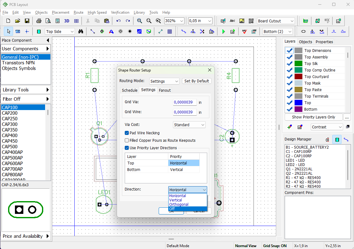
If you want to route a board with jumper wires you need to select the Grid Router, and check Allow Jumper Wires box in the Autorouter Setup dialog box. In our case, we don 't need that.
Select "Route / Routing Setup" from the main menu. In the pop-up dialog box, you can change the trace width and clearance between traces for default net class and the diameter of vias for default via style. Routing Setup dialog box is the quickest way to change these parameters, but more complex projects would require using several net classes and via styles. You can press All Classes... and All Styles... buttons to access the respective dialogs. We will discuss Net Classes and Via Styles later in this tutorial. On the Settings tab, the "Automatically Remove Loops" option is enabled by default. This allows traces to be optimized by removing closed loops. If you need to preserve loops on a specific trace, you can enable the "Do Not Remove Loops" option in Net Properties from the context menu.
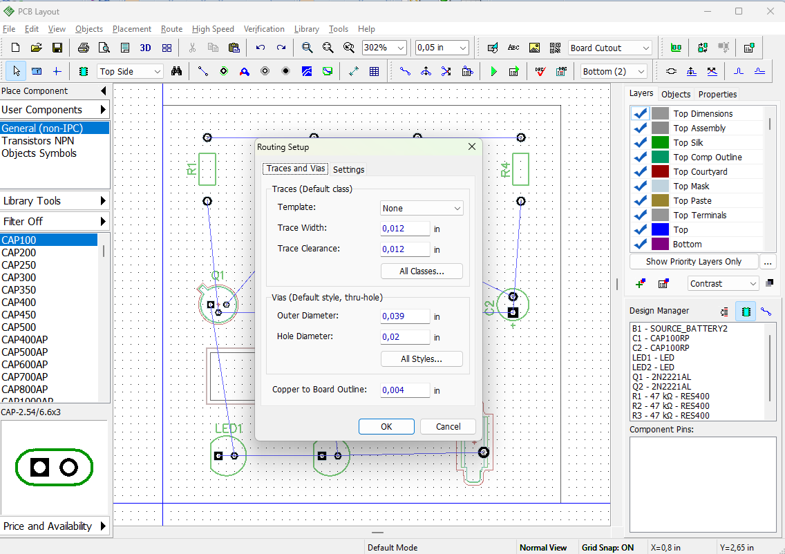
If you are new to DipTrace, we strongly recommend you to use the settings like in the picture above for this tutorial project, it will help to avoid any misunderstandings and errors later. Press OK to close this dialog box and apply changes, then set the grid size back to 0.05 inch.
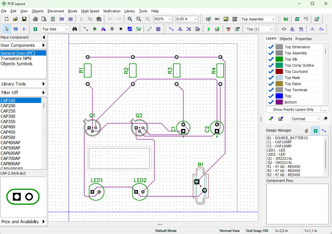
Now it's time to route the circuit board. Select "Route / Run Autorouter" from the main menu. You'll get something like in the picture below. Your layout doesn't have to be exactly like the one shown, so don't be confused if you are new to PCB design and some traces don't coincide with the picture.
Notice that the color of the traces depends on the layer color. We will change it in the next topic of this tutorial.
Automatic DRC
DipTrace has several verification options on different levels of PCB design. For example, Design Rule Check (DRC). It verifies object sizes, length/phase parameters of high-speed nets, and clearances between different objects according to user-defined rules. The DRC results are shown in the error-report list. Violations are marked with red and magenta circles directly on the design area. Design Rule Check in DipTrace operates in regular (offline) and Real-Time modes. If Real-Time DRC is active, you've probably noticed some red circles while moving components and creating traces. But it should be OFF by default, therefore we will discuss verification procedures later.
Regular or Offline DRC (Design Rule Check) runs automatically after autorouting. This project is very simple and you shouldn't get any errors, if there are some, make corrections and relaunch the DRC by selecting "Verification / Check Design Rules" from the main menu or press  button on the instruments toolbar. To change design rules, select "Verification / Design Rules" from the main menu. To hide error circles on the design area, select "Verification / Hide Errors". To disable automatic DRC after autorouting, uncheck the corresponding checkbox in the "Route / Current Autorouter" main menu item.
Select "File / Save" from the main menu, in the pop-up dialog box define the folder, type in the name of the file and press Save. You can save the design in XML format if version control is required.
Notice that now you can skip all topics till the Printing, because your PCB is actually ready for output, but if you want to learn some basic useful features of the DipTrace PCB Layout, we don't recommend to skip those.
11. Working with layers
The traces are in lower contrast, because they are on the Bottom layer of the board, while the Top layer is active. We can see those traces because the Contrast layer display mode and 50% opacity between the layers are default settings.
|
|
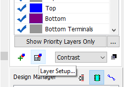
Look at the Layers tab on the Design Manager (press Ctrl+2 hotkeys if the Design Manager panel is hidden). First of all, you can organize the layers to your convenience here by selecting the priority layers and arranging their order in the list. Press |
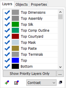
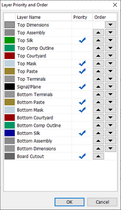
If you want to switch to another layer, double click it in the list or press the corresponding hotkey, or you can also use T and B keys for top and bottom layers respectively. Active layer can also be changed in the list box near the DRC control buttons.
We double click the Bottom layer in the list to activate it. Make sure you click on the layer name (text) in the list, not on the blue check mark or elsewhere. Click on the colored rectangle right next to the Bottom layer and select a color in the pop-up dialog box. Press OK to set the bottom layer color. You can change colors of other layers, if you like.
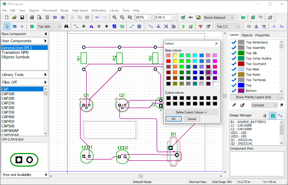
All layers are divided into two basic types: Signal layers and Non-Signal layers. DipTrace user can easily add, delete, and edit both. Our project is a simple circuit board with two signal layers: Top and Bottom. But as you can see in the list, there are much more of them. Assembly, Silk, Paste, Mask, etc. are non-signal layers. DipTrace creates them automatically on both sides of the board (and gives corresponding names to each of them depending on their side of the circuit board - Top Silk, Bottom Paste etc.). Each layer carries a special type of information.
Top/Bottom Silk are silkscreen layers, all texts and graphical information are automatically added there. Top/Bottom Mask and Paste layers contain information about solder mask and solder paste application zones. Some non-signal layers are necessary for correct board manufacturing, others provide additional functionality, for example, when drilling PCBs at home. More information about each layer in the Gerber Output topic of this tutorial.
Signal layers
Traces and copper pours can be created only on signal layers. There are two types of signal layers: Signal and Plane. Signal layers usually contain traces and sometimes copper pours, while Plane layers are inner (inside the board), they contain one or several copper pours. Autorouter can create traces only on signal layers.
|
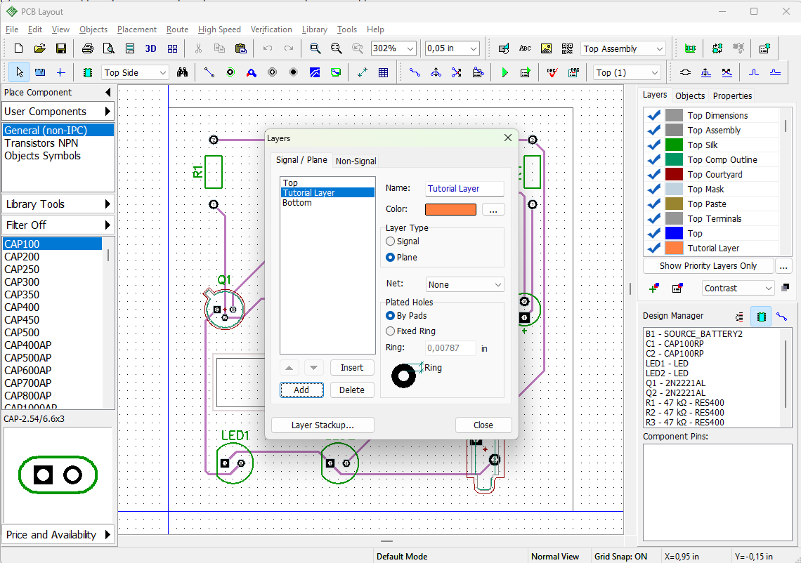
If you want to add, edit, create or delete a layer, go to "Route / Layer Setup" or press |
We will add a new plane layer called "Tutorial Layer" just to show you how it works. Press Add button in the Layers dialog box, then enter the layer name, select type and color. Press OK to create a new layer, now it appears in the list. Plane layers can be connected to one of the nets, usually Ground or Power, in our case it is unconnected. You can also define a single size for all pad rings on the layer. All pads on inner layers are always round.
Press the Close button to close the Layers dialog box, as you can see the Tutorial Layer is already on the layers panel, between Top and Bottom layers.
Right-click on any layer in the list to open a submenu for quick editing of the list and layers. Click on the color rectangle to quickly change the color of the corresponding layer.
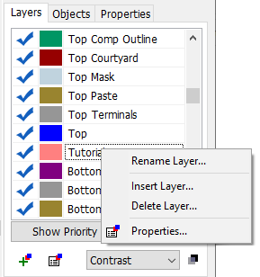
Insert Another plane layer and Call it Tutorial Layer 2.
Non-Signal layers
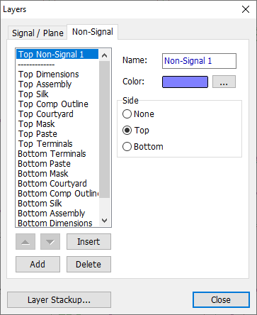
|
Customizable non-signal layers are used for various engineering purposes. They improve speed and total convenience of electronic design in DipTrace. If you need to create a non-signal layer, select the Non-Signal tab in the Layers dialog box ("Route / Layer Setup" from the main menu), then press the Add button, enter layer name, select color and layer side: None, Top or Bottom. None means that layer will not be locked to some specific side of the board. We do not need any custom non-signal layers. Close this dialog box. There are some quick-access buttons on the Layers tab of the Design Manager:
|
 – Add Layer;
 – Layer Setup;
 – layer display mode;
 – contrast level setup.
Remember to use 1,2,3, ... hotkeys to quickly change an active signal/ plane layer.
Notice that in DipTrace you see the bottom layer of the circuit board like if it was transparent. Pick "View / Mirror" from the main menu to mirror entire circuit board. Now you see how the bottom layer actually looks like. However, this is not necessary, because Gerber Export automatically creates the correct copper layout on the bottom layer.
Delete non-signal layer if you have created one, we don't need it for this project. But do not delete custom plane layers. Save the design.
12. Working with vias
DipTrace supports through and blind/buried vias (if divided by physical properties). Vias are also divided by two logical types that don't depend on their physical properties:
Trace Vias (regular vias), which are technically parts of the traces and appear automatically when you move trace segment to another layer;
Static Vias (similar to pads), which are placed manually, they have much more variable properties than trace vias.
All vias in DipTrace, disregarding their logical type, are organized to Via Styles.
We don't need a lot of different via styles for the current project, but we will add some in order to teach you the basic principles of working with vias.
Let's create two additional via styles: one with blind/buried vias of the same size as the Default via style (0.039 inch-diameter and 0.02-inch hole), and the other via style for through vias of bigger diameter. Go to "Route / Via styles" and check if Default via style has aforementioned parameters. Change them if you need. Then press Add button to add a new via style. It will appear under the Default one. Left-click it, and type in the name, change via type to Blind/Buried, and specify the layers involved (top and bottom layer of the via). In our case, we make blind vias from Top layer to Tutorial Layer. Specify via properties like in the picture below. Blind vias are impossible on printed circuit boards with only two layers, that is why we did not delete tutorial layers from the previous topic of this tutorial.
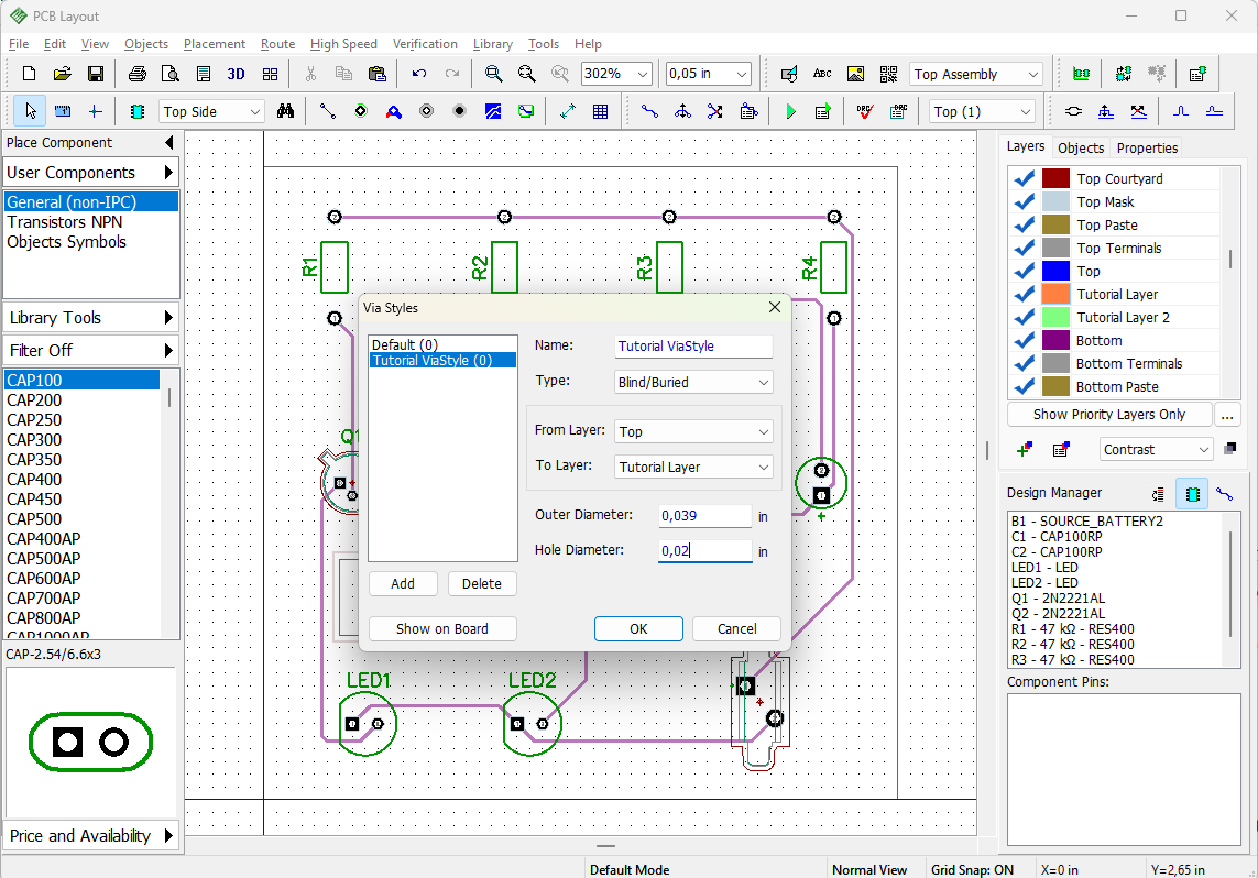
Now add one more through via style called "Tutorial ViaStyle2", and enter 0.065 inch outer and 0.03 inch hole diameters. Press OK.
Trace vias
Now unroute one of the nets (we will route it manually). We have chosen the net that connects resistors' pads with the battery.
Switch to the Bottom layer, then right-click on the net that you want to unroute, and select Unroute Net from the submenu.
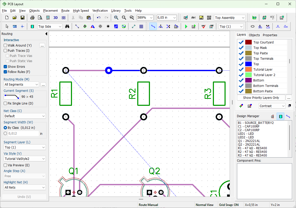
Go to "Route / Manual Routing / Add Trace" from the main menu or press the Tilde Sign (~) hotkey. You can enable the display of pad numbers in the View / Pad Markings menu. Left-click on the first pad (R1:2), to start routing a trace and draw it to some point between the R1 and R2. Use V hotkey and select Tutorial ViaStyle2 from the pop-up menu to apply it to the vias that will be created when changing layers. Auto means that DipTrace will use a via style that takes less space on the board, but in our case, we select the style with bigger vias (Tutorial Via Style2). Let's check Via Preview option on the Routing panel (alternatively, E button can be used). You can see that a circle, meeting the parameters of the selected via style, has appeared at the tip of the trace. Now left-click to set a trace segment between the pads, then right-click, and select "Segment Layer / Top" from the drop-down submenu (if you're routing on the bottom layer and vice versa). Trace via will appear automatically. Disable via preview with E hotkey and continue routing on the opposite side of the board to another pad (R2:2), and then left-click it. Create one more segment between the R2 and R3 components. Notice that trace color is defined by the layer color. Do not route the entire net all the way to the battery.
Static vias
You can use  button to place a new static via on the design area or you make one directly from a trace via - just right-click on it, and select Convert Via to Static. Then specify which vias to convert: Current via, Selected segments etc. Static vias behave almost like pads.
If you change the parameters of some via style, all vias of that style, even those on the design area, will change automatically.
We can change style, type, diameter of the static via and apply new settings to the current or selected vias or nets in the Via Properties dialog box. Right-click on one or several vias (or nets with static or trace vias), and select Via Properties from the submenu, make some changes, and press OK. If there is no via style with the parameters you've entered, DipTrace will ask if you want to create a new via style.
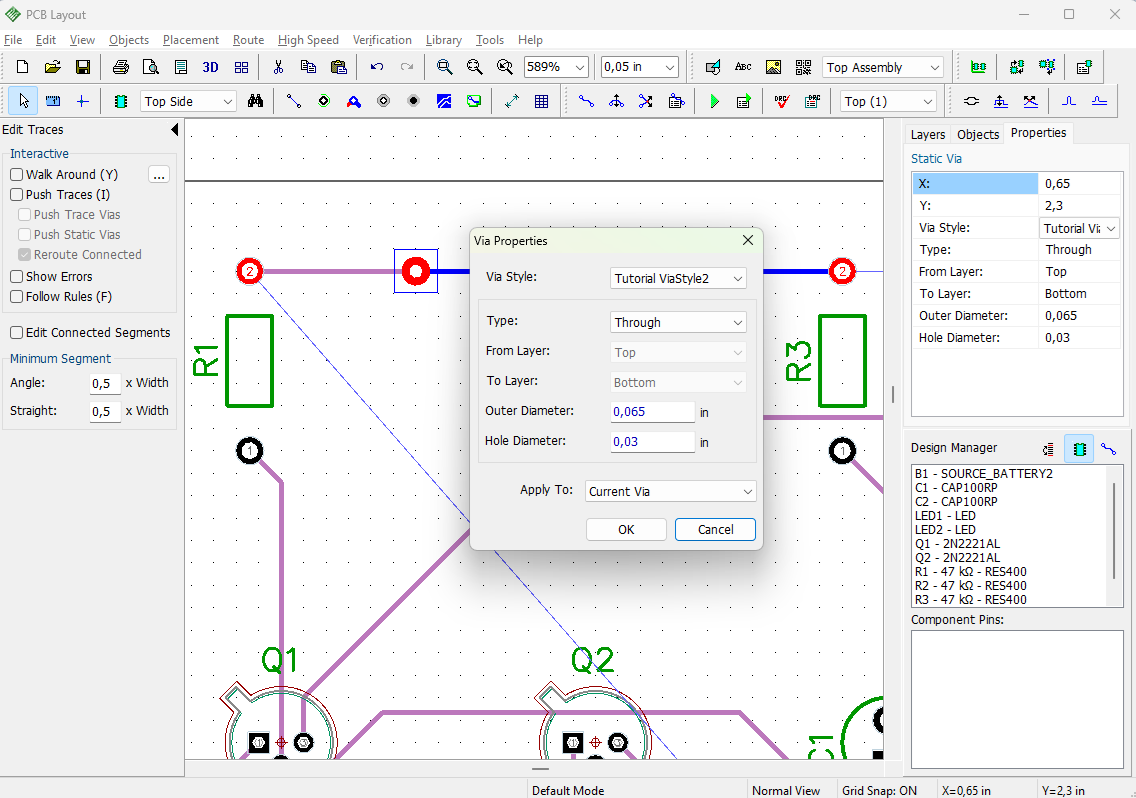
You can convert static vias back to trace vias - just right-click on the static via, and select Convert to Trace Via from the submenu, and select, which vias to convert. If you've placed a static via directly on the design area, you can not convert it to trace via.
Delete all vias, unroute the net again and route the trace on a single layer, but do not use the Undo tool, because this will delete custom via styles.
13. Net classes
All nets in DipTrace are organized to Net classes. Net classes allow the user to apply numerous parameters to any net with one click. Net classes work with manual and automatic routing (Autorouters). Specify net class parameters before routing nets.
We are going to practice in working with net classes using the same project, therefore, we need to completely unroute it first. Go to "Route / Unroute All" from the main menu. Then select "Route / Net Classes" from the main menu to open the Net Classes dialog box. You can see that only Default net class is available and all nets belong to this class. Press Add button and a new net class appears in the list of all net classes, right under the Default. Left-click it, and type in the name.
In the Class Properties tab, specify trace parameters and clearance value. In our case, we will make traces of a new net class significantly larger (0.03 in) with 0.05 in clearance.
Notice that asterisk symbol (*) in the input field means that it is a default value.
If you uncheck All Layers, the list under this checkbox becomes active, allowing different trace parameters on different layers of the board. We don't need this now.
Uncheck Use All Styles checkbox in the Via Styles section, and choose, which via styles you want to use with this net class. Just press << and >> buttons to add or delete via styles to/from the list of the active ones. The  button allows the user to preview parameters of each via style. We have allowed only custom via styles for this net class (see the picture below).
New net class exists, but it does not have any sense if no nets belong to it. So we're going to add nets. In the lower-right of the Net Classes dialog box, you can see the list of all project nets and the name of the current net class of each net in the brackets. In our case, it is Default net class. Select one or several nets with Ctrl key, and press the  button to add them to the net class (Class Nets list right above).
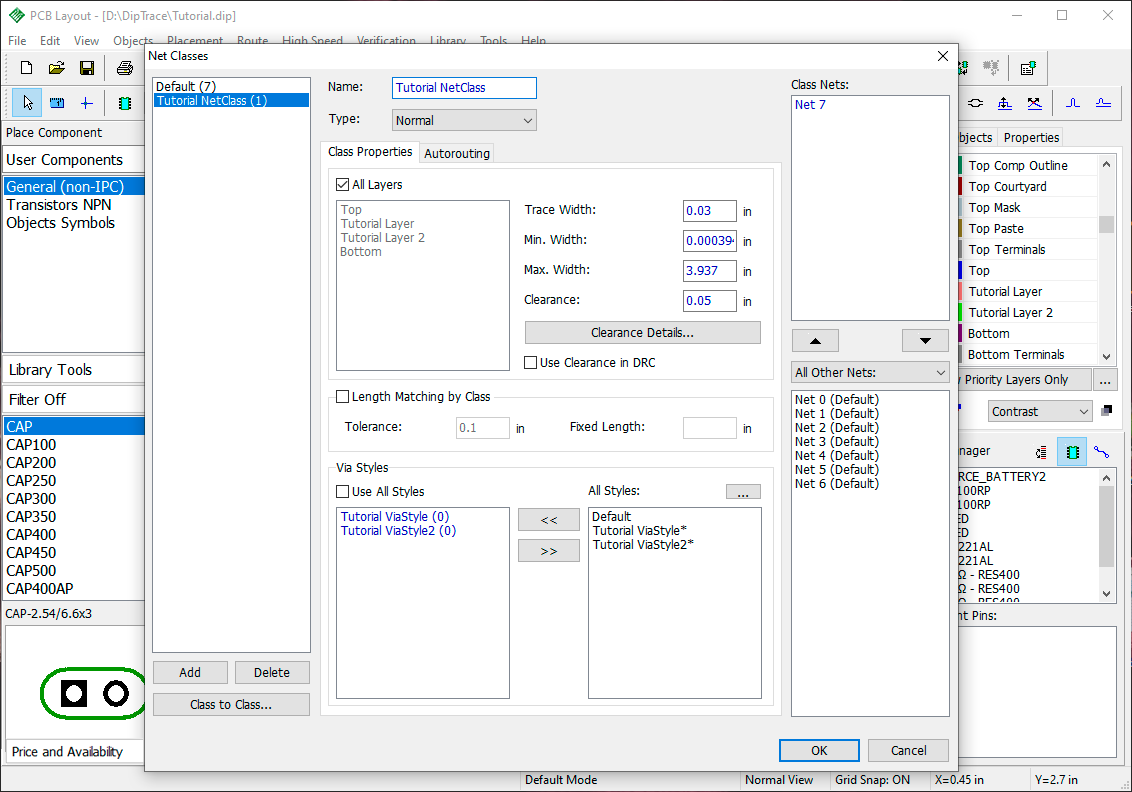
As you can see, the Tutorial NetClass contains one net (Net 7 in our case) with .03 inch trace width.
The Clearance Details button allows you to set different clearances depending on the type of the objects. Press Class to Class to specify clearance between the nets of different net classes. Class to class clearance is used by DRC and has priority over regular net class clearances. Make sure Use Clearance in DRC item is unchecked, and press OK to close the Net Classes dialog box and save changes.
Autorouting with net classes
Now you have two different net classes, one net belongs to Tutorial Net Class and the rest – to Default. It's time to route the board with autorouter, select "Route / Run Autorouter" from the main menu or press Ctrl+F9 hotkeys and you'll get something like in the picture below. As you can see, the traces on the PCB have different width, because they belong to different net classes with different parameters.
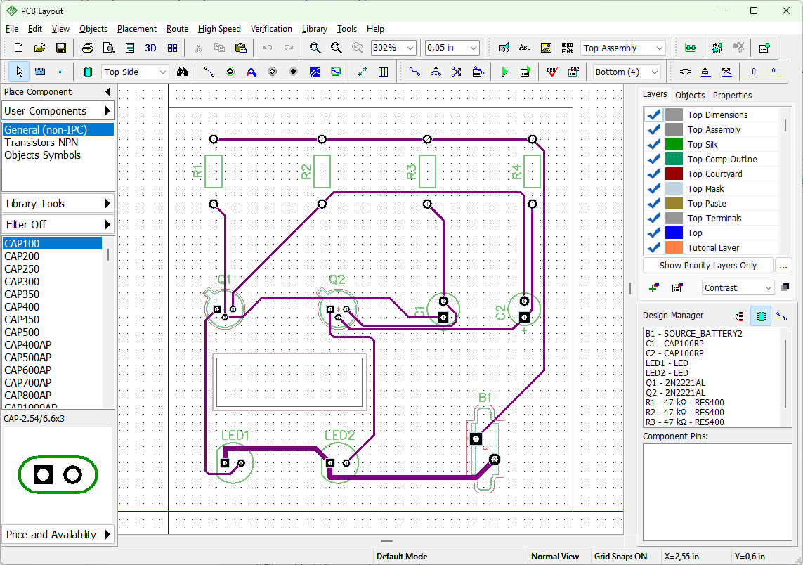
Now unroute the board again ("Route / Unroute All"), open the Net Classes dialog box and reassign Net 7 from Tutorial NetClass to Default class (use the  button). Press OK, then launch autorouter again and you'll get the circuit board with all traces of the same width. Tutorial NetClass still exists, but it doesn't do anything because no nets belong to it.
Manual routing with net classes
Select the Bottom layer, and left-click on one of the nets (for example, Net 6 between the resistors and the battery), you'll see the Net Properties panel on the Design Manager on the right. In the Net Class drop-down list select Tutorial Net Class. Then right-click on the same net and select Unroute Net from the submenu. Now press the Tilde Sign (~) hotkey to activate manual routing mode, left-click on the first pad (R1:2), and create a trace to another pad (R2:2) left-click it to create a trace segment. You'll notice that the trace is much wider because it belongs to another net class.
Notice that DipTrace allows for changing the net class of the routed net, but in order to apply changes, the net has to be unrouted and routed again.
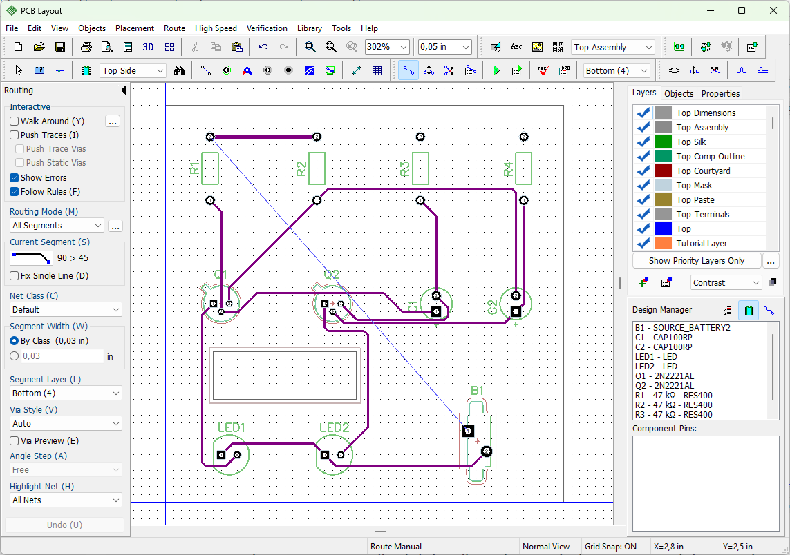
We don't need that trace width diversity on the board. Please Undo (Ctrl+Z) several times or manually delete all custom net classes, via styles, and inner layers to get the layout right after autorouting.
Save the project ("File / Save" from the main menu). You can save the design in XML format if version control is required.
Manual routing and measurement
14. Manual routing
Simple projects like ours can be routed automatically, but for complex boards, manual routing is a must. Actually, the entire board can be routed manually, but because of low speed of manual routing a combination of the two methods is usually the best choice for complex projects. This allows the designer not only to get a working prototype, but also to accomplish the project in reasonable terms. Critical nets are routed manually and the rest – with autorouter.
Our simple board is already good enough, but we're not done with practicing yet. Moreover, sometimes you may need to correct traces after the autorouter.
Manual routing panel
Manual routing offers complete control over your design and allows you to make adjustments that automated tools might miss. However, with this flexibility comes the responsibility of carefully managing any rule violations you may introduce. DipTrace helps streamline this process with interactive tools, allowing you to push traces, avoid obstacles, validate your design in real time or block actions that would conflict with your design rules.
To access these features, click the Route Manual button  . The Routing panel will appear on the left. Let’s explore some of the Basic Interactive tools.
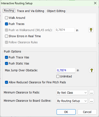
The Push Traces tool automatically shifts existing traces, making it easier to route the current net optimally. To try this out, enable Push Traces on the Routing panel and click  button to its right. This opens the Interactive Routing Setup dialog, which can also be accessed via Route > Interactive Routing in the main menu. In the pop-up dialog box, select "Push Traces" on the Routing tab.
Make sure that both Push Trace Vias and Push Static Vias options are checked. This will enable the software to relocate vias while routing.
Next, let’s configure the Jump Over Other Objects feature, which determines how far the software will search for placement options jumping over obstacles on the board. Set this distance to 0.5 inches.
Our project is quite simple, however, more complex designs may require fine-tuning. You can enable Reduce Pad Clearance for Smaller Pad Pitch if needed, and choose whether the Allowed Clearance to Pads will be governed by Net Class or Design Rules.
Once you've made these adjustments, press OK to apply the settings.
Right-click on one of the nets and select Unroute Net from the submenu. In this example, we've chosen Net 6, but feel free to select any net you prefer. The Unroute Net command will apply to all selected nets.
Now, left-click on any pad belonging to the unrouted net and begin routing a trace toward existing routed traces. You’ll notice that as you route, DipTrace automatically pushes and reroutes existing traces to accommodate the new path. In some cases, routed traces will jump over other objects on the board to make room for the new one.
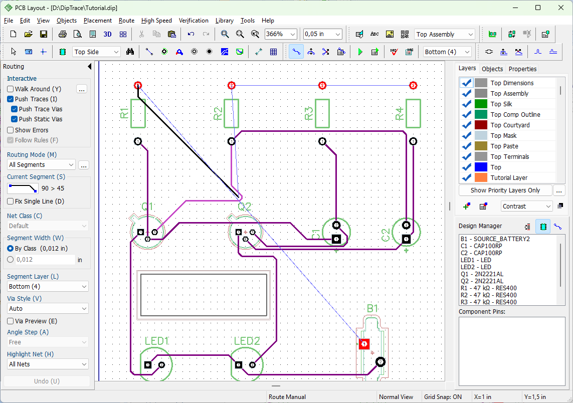
Disable the Push Traces option to explore the next interactive feature: Walk Around
The Walk Around tool automatically routes traces around existing objects, avoiding obstacles during routing. To try this out, enable Walk Around on the Routing panel. Now, left-click on any pad belonging to the unrouted net and begin routing a trace by simply moving the mouse in the desired direction. DipTrace will automatically create the trace, routing it around existing obstacles. Move the cursor to pad B1:1 and left-click to complete routing the trace. Notice that the blue ratlines are no longer displayed on pads R2:2 and R3:2, as they have been automatically connected to the new trace.
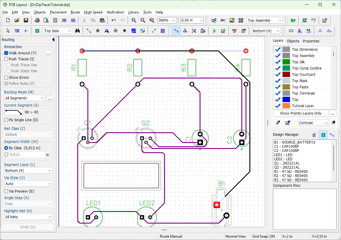
It is recommended to use Walk Around and Push Traces simultaneously. In this case, the router will choose the more optimal behavior: it will push existing traces where efficient, or walk around obstacles when that provides a better route. The Push vs Walkaround parameter on the Routing tab in the Interactive Routing Setup defines the balance between push-based routing in tight areas and walkaround routing with increased trace length to minimize trace pushing.
Undo the last routing action (Ctrl+Z), then disable the Walk Around option to explore the next interactive feature: Show Errors.
When enabled, any routing errors will be highlighted in real time with red circles as you route or edit traces. If the Follow Rules option is also activated, DipTrace will prevent any violations of your pre-set design rules while routing.
Let’s continue working with Net 6. Left-click on any pad associated with it and intentionally route a trace over other existing traces. You’ll notice red circles appear to indicate errors. Now, enable the Follow Rules option, and you’ll see that any trace segment violating the design rules turns into a dotted line, preventing you from placing it.
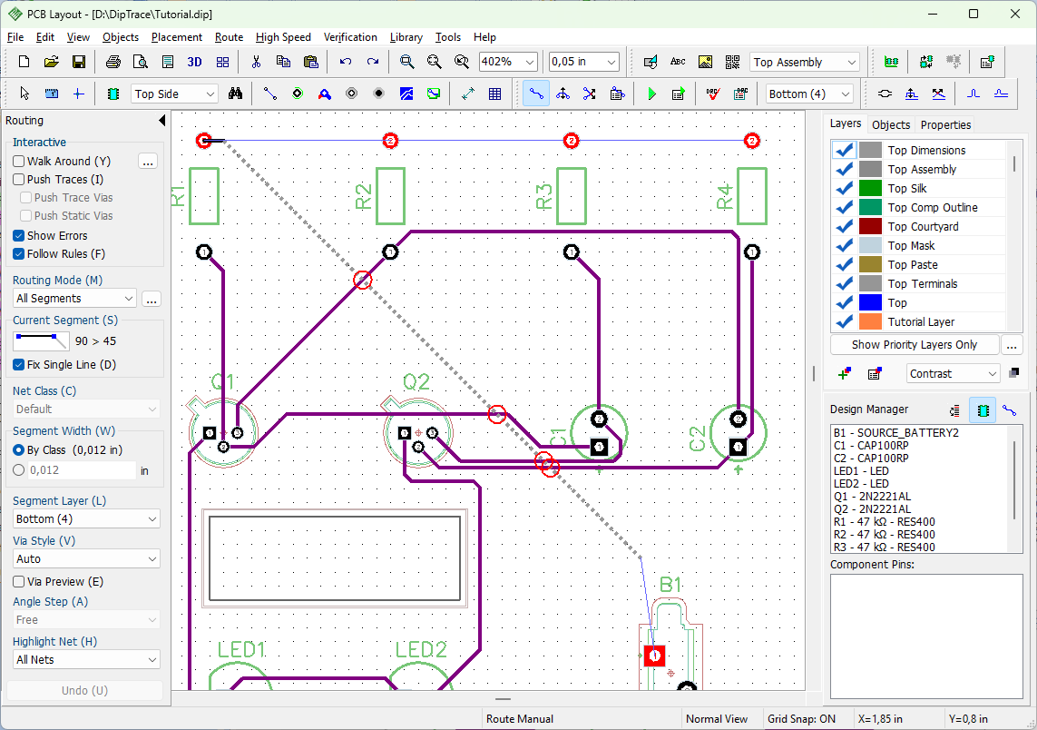
The rules defined in DRC are applied. DRC will be discussed in more detail laterNow right-click and select Cancel from the submenu or press Esc key to eliminate the trace we tried to route.
It's time to practice more in manual routing. Note that in the Routing Mode list (on the Routing panel) you can specify the group of trace segments that you are going to need for routing, therefore, you will be able to select the current segment not from the list of all segments, but from the list of segments of one mode. To do this, you should customize My Routing Mode.
Select All Segments routing mode, then left-click in the Current segment field and select 3-point Arc. Left-click on one of the pads of the unrouted net, then left-click on the second pad and move the mouse to adjust the radius of the arc and fix it with a left click.
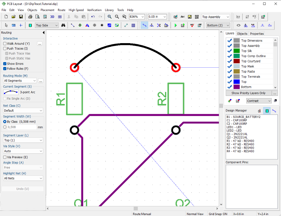
Our project is very simple, but when working on a more complex one you may find it quite handy to fix only one part of polyline and rounded line segments when routing a trace. Enable Fix Single line option on the Routing panel or use D hotkey, if you want the software to place only the first part of the segment and leave the second one in the routing mode. You can change Route mode to 90/45 Lines to check out this option.
Do not try to change the net class of the existing net on the Routing panel, net class should be defined in the Net Properties or Net Classes dialog boxes before routing.
Notice that you cannot change net class of the existing net on the Routing Panel. This change will be ignored and applied only to a newly created net. Don't forget that net exists irrelative of whether it is routed or not.
We have only one net class to avoid confusion and concentrate on the subject.
DipTrace allows changing the layer of the trace being routed. Undo the arc segment or right-click on it and select Unroute Segment from the submenu, you can also select the segment and hit Del hotkey. Set 90/45 Lines routing mode, left-click on the first pad (R1:2) and draw a trace to some point between the first and the second (R2:2) pad, left-click to anchor it. Now activate Via Preview by pressing E hotkey. Use V key to change Style of the trace via that will be placed automatically when routing layer is changed.
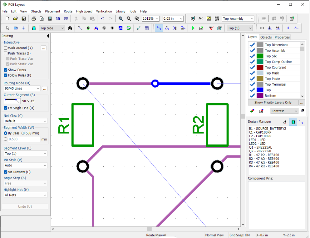
Press 1 to change the layer and E to disable Via Preview. Connect the trace to the R2:2 pad.
On the Routing panel, you can choose, which nets to highlight. If you highlight only the current net – no other nets will glow, even if you touch them with a new trace.
You can undo by pressing the U hotkey while routing. Notice that there are hotkeys that will make manual routing really easy and quick.
Y - enable/ disable Walk Around tool,
I - enable/ disable Push Traces tool,
F - enable/ disable Follow Rules option,
M – switch between routing modes,
S – change current segment,
D – fix only the first angle-forming segment of polylines and rounded lines,
W – set trace width,
T – switch to Top layer,
B – switch to Bottom layer,
L – change segment layer,
J – switch to jumper wire or back (if you are in Bottom layer, jumper will be placed to Top and vice versa),
V – toggle between via styles,
E – preview trace via before placement,
A – angle step,
H – highlight net,
P – pause routing; once the routing is paused, you can edit the layout and then resume routing by hitting P key again,
1 – 0 in the top of keyboard – switching between layers (up to 9).
Go to "Tools / Hotkey Settings" from the main menu to view and change the hotkeys. Refer to the PCB Layout Help document ("Help / PCB Layout Help") for more details about custom keyboard shortcuts and manual routing.
Now please Undo (Ctrl+Z) several times or change the layout to the state after autorouting (no net classes, via styles, new layers etc.).
Editing modes
You already know how to create traces ("Route / Manual Routing / Add Trace" from the main menu or pressing button; left-click on the first pad to start routing, and another click on the next pad to create a trace). Always make sure that a correct layer (Bottom in our case) is selected.
Editing traces is a bit different. Press  button or simply left-click on the trace and drag it to another location and drop it. The Edit Traces mode allows the user to move traces, respecting 45- or 90-degree angles. This is very convenient for almost any design, but sometimes you might need traces editing tool with more capabilities. Go to "Route / Manual Routing / Free Edit Trace" from the main menu or press
  button on the Route toolbar. Now you can edit traces without any restrictions.
Don't forget to set the grid size (with the  drop-down on the Standard toolbar or Ctrl+Plus Sign and Ctrl+ Minus Sign hotkeys). To configure the list of available grids, select "View / Customize Grid" from the main menu. F11 hotkey hides or shows the grid on the design area. You can adjust grid precision and set minimum grid size value in a dialogue, which pops-up when selecting "View/ Precision" item from the main menu.
Remember, if you don't know which tool you are working with, right-click a couple times on a empty spot on the design area and DipTrace will return to the Default mode.
Nodes
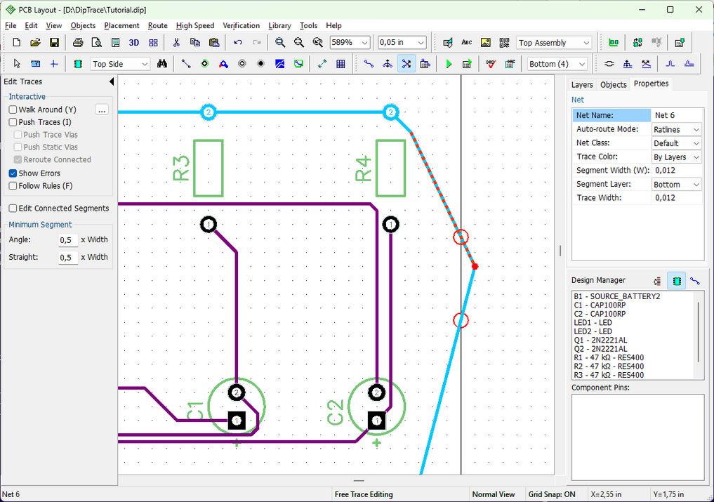
Any routed net is divided to traces (often called "tracks"). Trace is a copper track between two pads of the net. Trace (track) consists of segments. A segment is a route between two nodes. Node is a point on the route, which divides a trace into segments (red dot or a small square in the picture below). The designer can move existing nodes, add new ones or delete them. This gives more flexibility while editing traces. Left-click on a trace segment, and press N hotkey to add a new node in the selected place, then left-click it and drag to some point outside the board outline (Free Edit Mode in the picture below).
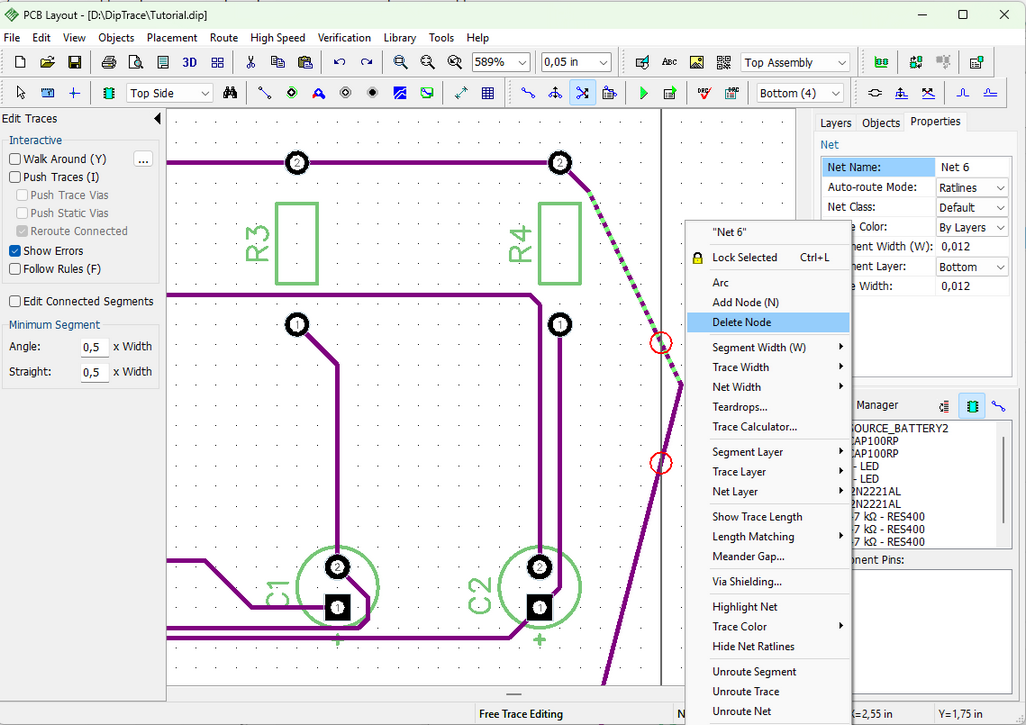
Undo free editing and right-click on the design area to return to default mode. If you don't need some node anymore, you can delete it – right-click on the node, and select Delete Node from the submenu. In the same submenu, you can change the name, color, width, and the layer of the net, trace or segment etc.
Change layer
DipTrace allows moving an existing net (trace or trace segment) to another layer - right-click on a trace segment of some net, and select "Segment Layer / Top" or use the Segment Layer drop-down list in the Net Properties panel on the Design Manager. Trace vias appear automatically. You can choose several segments of the same or different nets with Ctrl or Shift buttons and change their properties at a time.
Note that you can use Tab hotkey to toggle between the selection of a segment, a trace or the entire net.
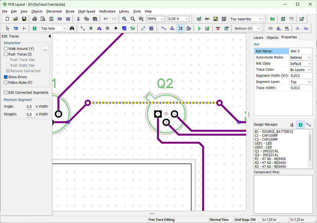
Edit Traces width Walk Around & Push Traces
In trace editing mode, Walk Around and Push Traces can be used similarly to interactive routing. The corresponding settings are available on the Trace and Via Editing tab in the Interactive Routing Setup.
If you need to move or rotate an object (such as a component, mounting hole, etc.), Walk Around and Push Traces can assist by automatically adjusting existing traces. The Walk Around and Push Traces settings for object editing mode are located on the Object Editing tab in the Interactive Routing Setup. If the object cannot be moved, disable the Follow Rules option (F hotkey).
Now return that segment back to the Bottom layer, and select the bottom layer.
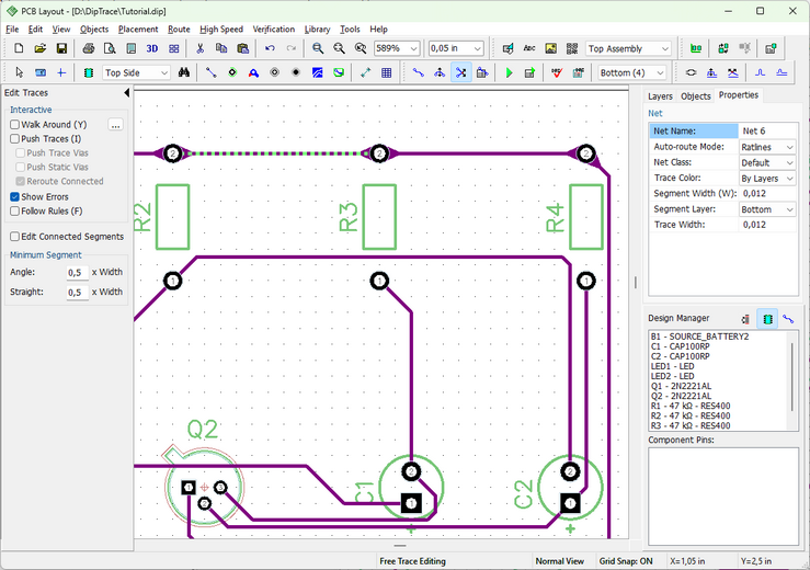
Teardrops
DipTrace allows creating teardrops, which are basically drop-shaped features at the junction of vias, pads and traces.The main purpose of teardrops is to enhance structural integrity in presence of thermal or mechanical stresses during fabrication as well as to enlarge manufacturing tolerances.
In PCB Layout you can define teardrop parameters as a function of the pad/ via or trace size and apply them to the selected object/-s.
Let's see, how to use this feature. Right-click on Net 6 on the design area or in the list of nets on the Design Manager panel and select Teardrops from the submenu. In the pop-up dialog tick Through-Hole Pads and Vias and set Length to 50% and Connection to 90% of pad size. We are not going to set teardrop parameters for SMD pads and trace to trace junctions because they are not any in our project. In the Apply to drop-down select Current Net. 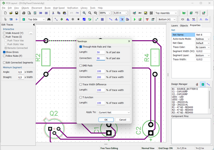
You can see that junctions between the traces and all through-hole pads, belonging to the Net 6, are now shaped like a drop.
Note that you can also add teardrops to individual pads or vias - just use a similar dialog, launched from the right-click submenu of the respective objects, to set their parameters.
Undo teardrops.
15. Measuring trace length
DipTrace allows for easy and convenient trace measuring. The current project is simple, therefore we don't need to use this tool, but if you design high-speed circuits with differential pair signaling, trace length becomes very important. This tool is often used with trace length matching tools, which we will review later.
Notice that hint of each trace can be configured to display its length: select Add Object Details in the View/ Display Hint submenu.
Please select several traces (you can use box selection or Ctrl button). Right-click on one of selected traces, and choose Show Trace Length from the submenu.
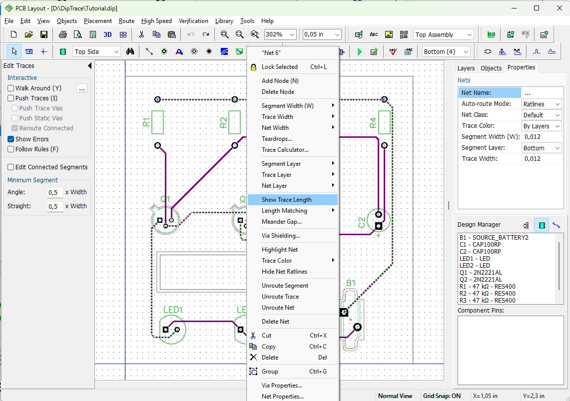
You will see the small boxes with trace length values near all pads of the selected nets, they are also highlighted when hovering over the trace with a mouse cursor. Values are in the current measurement units (inches in our case), they change in real-time when you edit the trace.
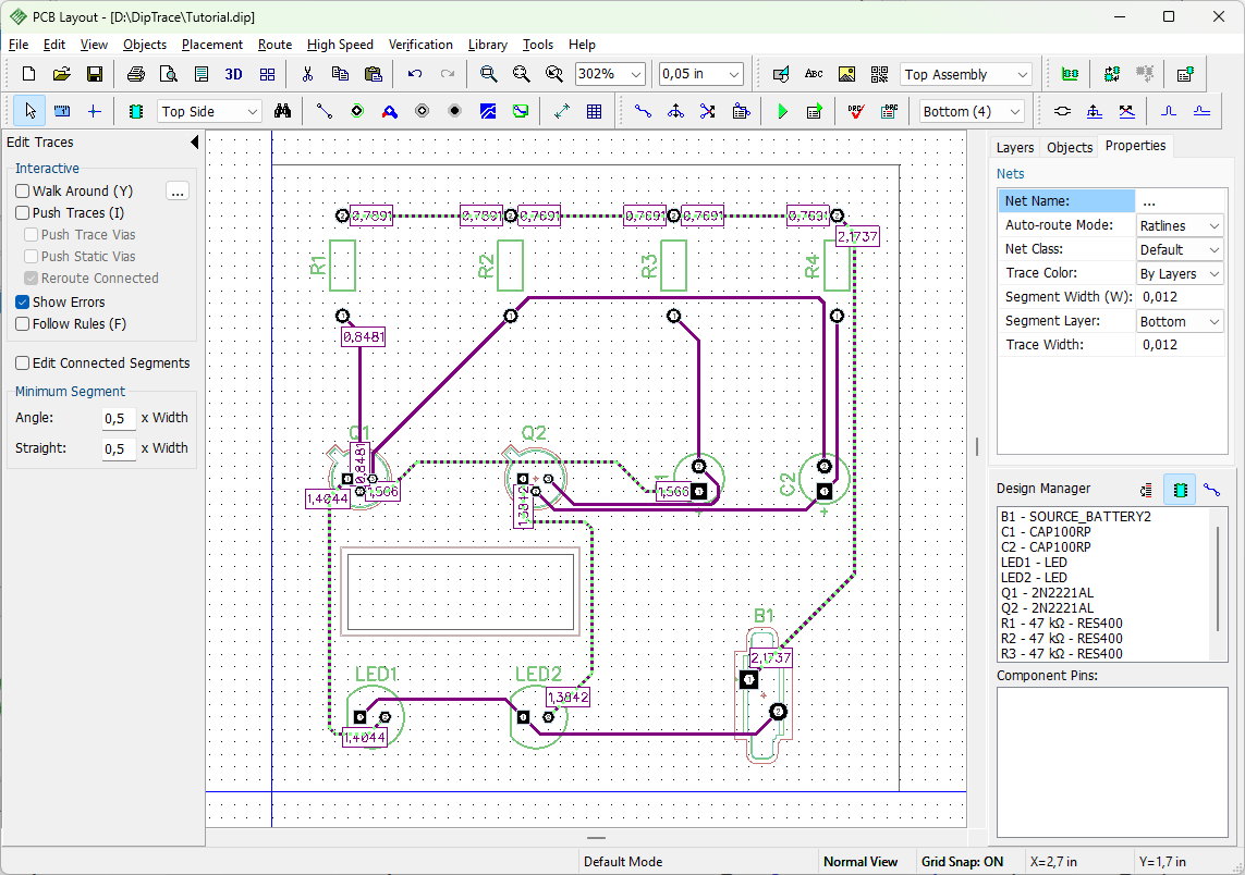
Notice that DipTrace can calculate a phase shift considering layer stackup (via height) and the length of bonding wires inside a component (determined by the Signal Delay).
By default, DipTrace does not consider these values for trace length calculation. If you want to consider them, go to "High Speed / Length Matching" from the main menu, then press button, and check Enable Layer Stackup and Enable Pad Delay in the Length and Phase Measurement Settings dialog box.
Now please hide the trace length boxes, using the net submenu (uncheck the same item) or Undo tool.
Working with board objects
16. Selecting objects by type/layer
Sometimes it is necessary to select all objects on one layer or exclusively components, nets, vias etc. With the current layout, it is very easy to do with the mouse and Ctrl key, but what if the layout is very complex?
Select "Edit / Edit Selection" from the main menu.
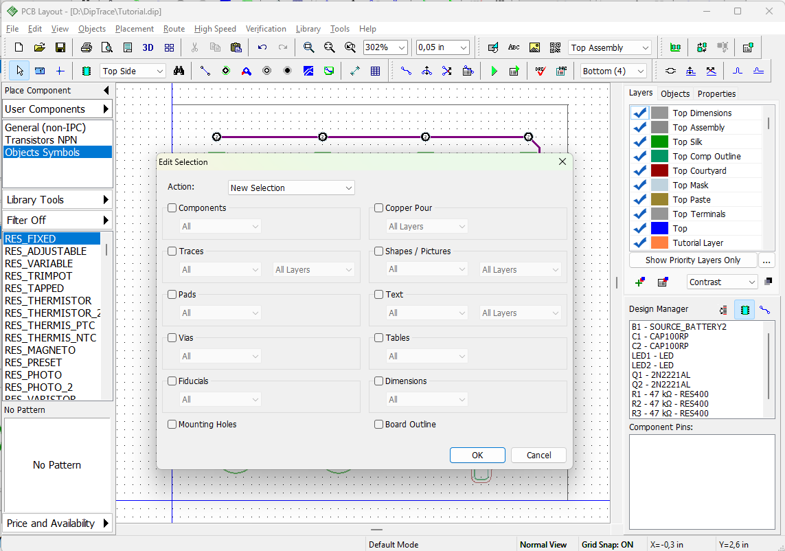
Check Components item, and click OK – all components are selected now.
Let's make it a bit harder and model a real-life situation, when we need to select only unconnected vias in the predefined area of the board.
First of all, deselect components with a right-click on an empty spot. Then place several static vias and connect only some of them to nets randomly, while leaving a couple of vias unconnected. Use "Objects / Place Static Via" from the main menu or button to place vias and "Objects / Place Ratline" or  button – to create connections visually. Left-click on the via, and then left-click on the pad to add via to the pad's net.
Now define selection area using the box selection. This box represents an area where we plan to select unconnected vias so we will not include all vias of the layout to this selection. Notice that we are on the Bottom layer, where we have all the traces.
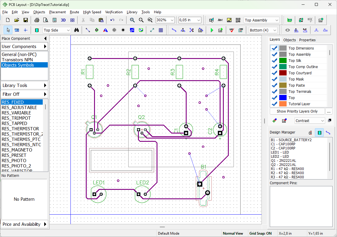
All objects in the box are selected. We need to extract only non-connected vias from the selection. Open "Edit / Edit Selection" dialog box, choose Action: Keep Selected, check only Vias checkbox (other boxes should be unchecked), and then select Not Connected from the Vias drop-down list. Click OK and only unconnected vias stay selected.
The next step could be connecting those vias to some net, all at a time. In real life, this feature can be used to connect ground net to plane/copper pours. Right-click on one of selected vias (it should be highlighted in red), select "Add to Net / Selected Vias" from the submenu, and specify the net in the pop-up dialog box.
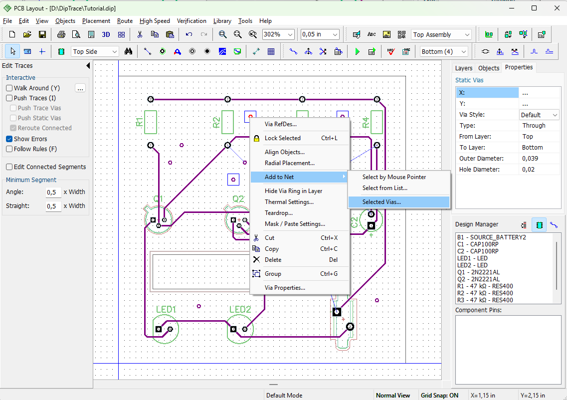
Choose some net from the list, and click OK. All selected vias will be connected. Remove all static vias from the board and return the circuit board to the previous state (select all vias and press Del key or Undo).
17. Placing text and graphics
With DipTrace you can add texts, shapes, and logos in BMP, DXF, JPEG or PNG formats directly on the board and export them to Gerber.
First, you have to select the layer where you're going to place graphics, usually, it's a silkscreen layer (Top Silk in our case). PCB Layout allows the user to change layers with two drop-down lists on the toolbar and in the Layers tab on the Design Manager panel. Double click Top Silk in the Layers tab of the Design Manager panel or select it from a drop-down.
Note that a drop-down list on the Drawing toolbar allows you to select any non-signal or Signal / Plane layer for placing graphics. If you have selected Signal / Plane layer, all shapes, texts and logos will appear on current signal/plane layer, which is specified with the drop-down list on the Route toolbar.
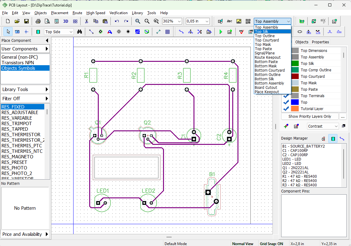
Let's make the board polygon a little bit bigger to place additional text at the top. Drag and drop upper-left and upper-right vertices of the board outline a little bit upwards. Make sure you click on the vertex point, not on the outline. DipTrace makes visual editing very easy with appropriate grid size.
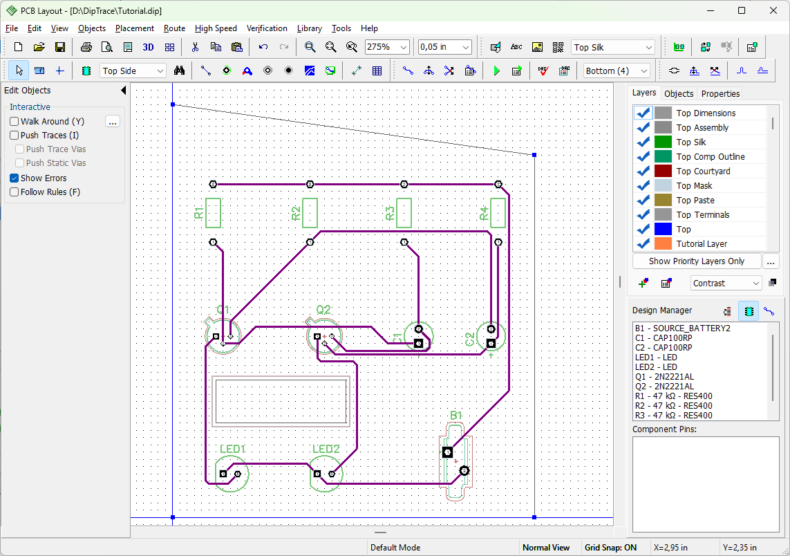
You can move the board outline. Left-click on the line (not the vertex), then drag and drop it.
Remember that if you can not highlight and edit certain objects, probably, you are not in the default mode. Therefore, right-click on a free area to cancel the current mode. Objects located on inactive layers of the board can’t be edited unless you are in the Contrast Edit layer display mode (View/ Layer Display/ Contrast Edit).
Press  button, left-click where you would like to place text, type it in, and press Enter to move to the next line. Right-click on a free spot to return to default mode.
Use the mouse or arrow keys to move the text object on the design area. You can easily resize the text by simply dragging its corner with the mouse. When a text object is selected, font settings, font type (Vector, TrueType), and text layer can be changed in the Text Properties tab on the Design Manager, or with the right-click submenu. Use vector font, because it is directly exported to Gerber. For Unicode and Non-English characters select TrueType fonts, however, these export to Gerber as small lines (created by a special recognition algorithm).
Some PCB manufacturers do not accept TrueType text objects in copper layers.
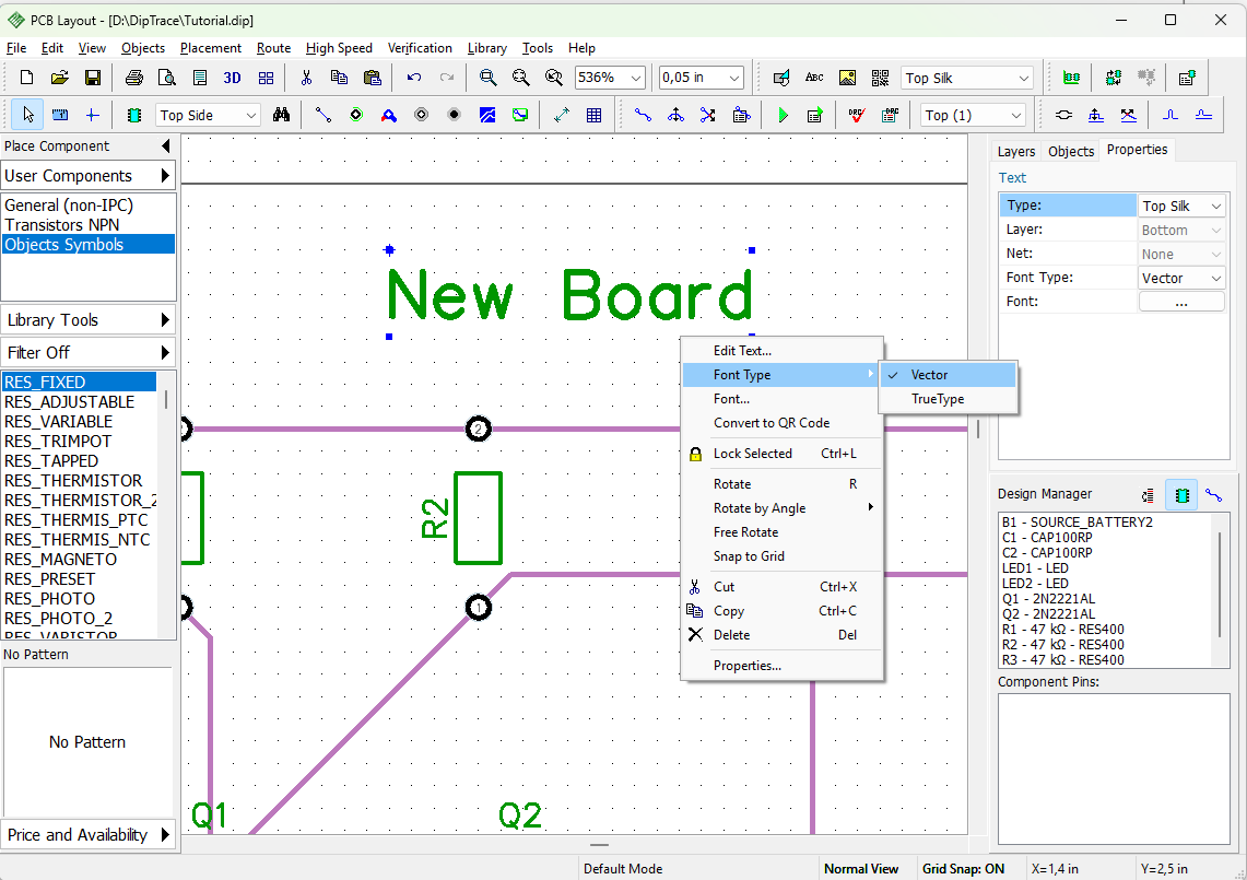
You can change all the parameters of the text object any time. Right-click it, and select Properties from the submenu.
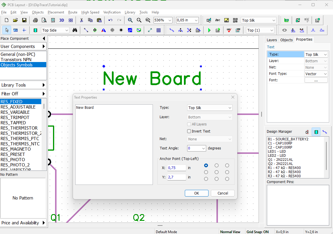
In the pop-up dialog box you can edit the text and its display parameters as well as rotation angle, location and coordinates of the anchor point. Select text object Type from the drop-down and move the object to another layer or define different properties (for example, create a route keepout used for autorouting, etc.). In our case, we just leave that text on the Top Silk layer.
Note that Invert Text option allows to place text as void in silk screen or copper pour.
Any text or URL can be placed as a QR code. Click "Place QR Code" on the Drawing toolbar or select Objects / Place QR Code from the main menu. Then left-click on the desired location in the workspace. In the pop-up dialog box, enter the required text or link, set the QR code Module Size (dot size), and choose the desired layer. For Signal/Plane layers, select the specific layer and whether the QR code should be connected to a net. Finally, click "Place".
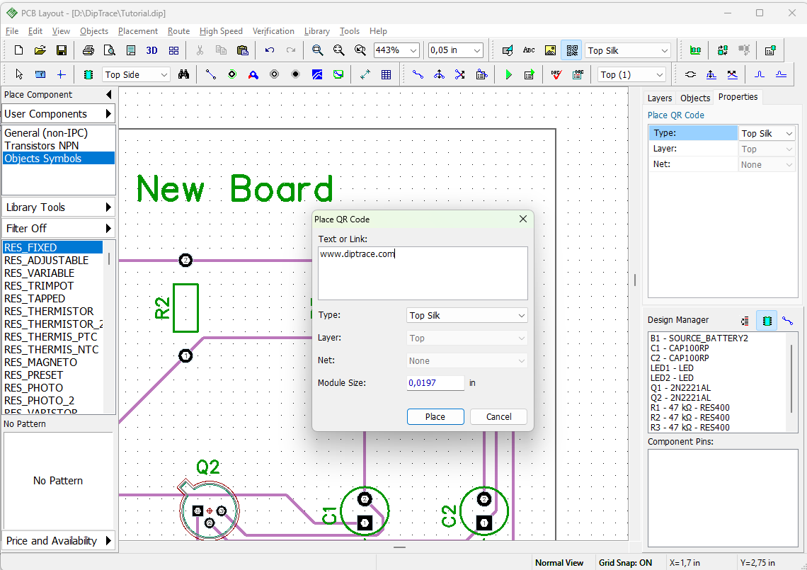
You can modify an existing QR code and its properties via its context menu by right-clicking on it. You can also convert any text to a QR code and back using the context menu.
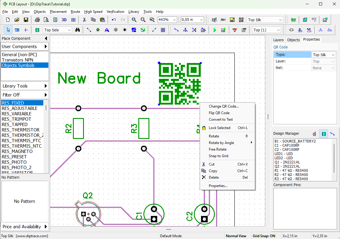
You can add shapes to assembly, mask, paste, signal, route keepout, board outline and cutout layers. The properties of the placed shapes can be defined via Shape Properties dialog box.
18. Copper pour
Copper Pour is used as a low-impedance conductor for Power and Ground nets. Pours are usually located on inner layers of the board, but they can be placed on top and bottom sides as well.
Place copper pour
Select the Bottom layer, then go to "Objects / Place Copper Pour" from the main menu or press  button on the Elements toolbar. Now you can draw a copper pour polygon borderline by defining its key points on the design area, then right-click on the last point of the polygon, and select Enter from the submenu to finish drawing. We need a copper pour that covers the entire bottom layer of the board. You can draw a precise polygon manually or create a random shape (for example, like in the picture below) and use the Depending on Board feature (Place Copper Pour dialog/ Border tab), which will pour the entire layer automatically, regardless of the initial shape. Place Copper Pour dialog box pops up when you select Enter from the submenu upon placing a copper pour border.
You can change the grid size up and down to your convenience at any point of copper pour placing/ editing.
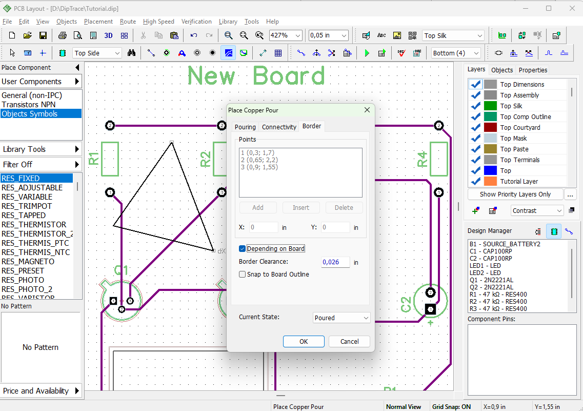
This dialog box has three tabs: Pouring, Connectivity, and Border.
Pouring tab allows you to specify different non-solid fills for the copper pour, clearance width, line width, line spacing, island removal options, pour priority, and current state (poured or unpoured). You can also apply net clearances as copper pour clearances by checking the corresponding item. DipTrace has shape-based copper pour system.
Connectivity tab – here you can connect copper pour to the net, select thermals and change their settings. DipTrace supports separate thermals for SMD pads. The Hide Net Ratlines regime can automatically show ratlines only for unconnected traces or other if specified.
Border tab allows you to define the border points and build the copper outline automatically.
Check Depending on Board checkbox and keep all other settings like in the picture above. The Snap to Board checkbox means that copper pour will resize depending on the board outline. Click OK to place a copper pour.
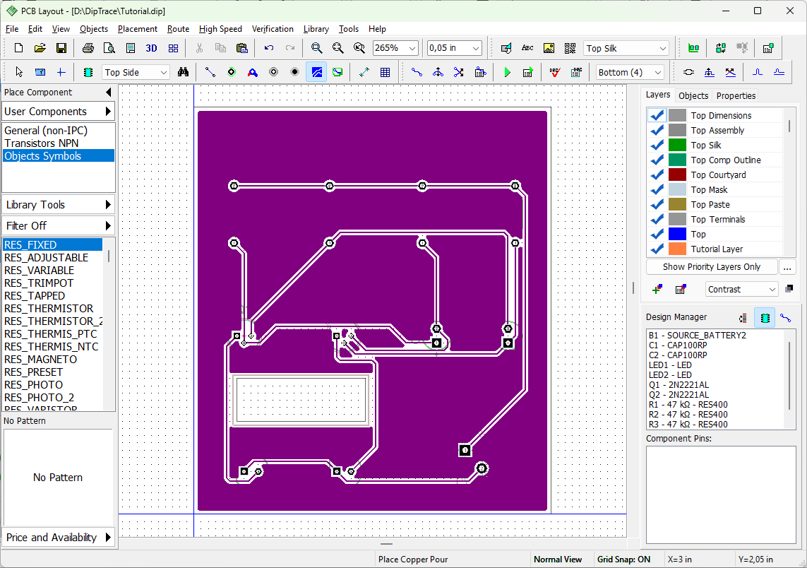
Board outline clearance specified in the copper pour settings is not applied to board cutouts. Always use route keepout to allow for a certain clearance between the copper pour and cutout, like we did before.
Copper pour can be in two states: Poured and Unpoured. The second state is often used for editing because only the copper pour border is visible in the Unpoured state. To change the copper pour state right-click on the copper outline (not on the copper pour body), select State from the submenu, and choose the item you need.
As you can see, we have a copper pour, but it is not connecting any net. Now we will practice and connect two different nets using two copper pours on the Bottom layer. Copper pour priority option will help us to achieve our goal.
Connect copper pour
Unroute one of the nets (for example, Net 6, which connects resistors to the battery), right-click on the trace, and select Unroute Net from the submenu. Remember the net name ("Net 6"). Right-click on the copper pour border, and select Properties from the submenu. Go to the Connectivity tab, and select Connect to Net: Net 6, then select appropriate thermals (for example, 4 spoke), and press OK to update the copper pour.
Notice that you should click directly on the copper pour border (not on the copper body or the board outline) in order to open copper pour properties dialog box.
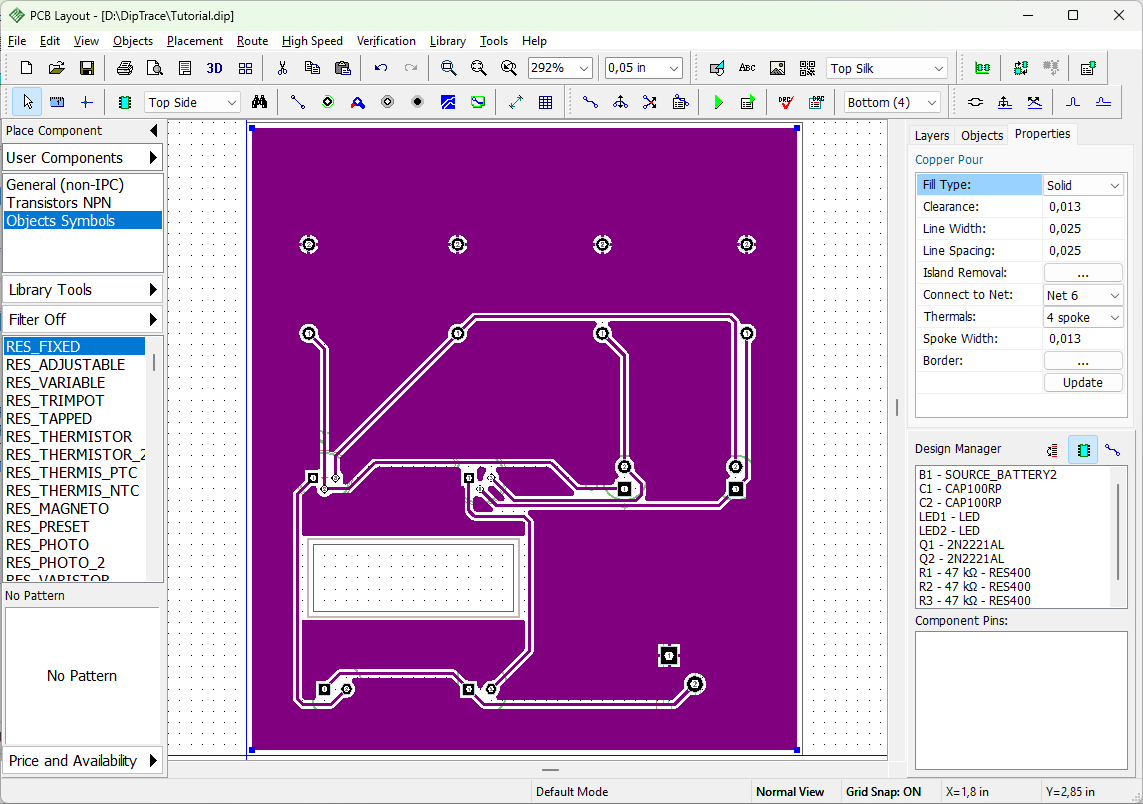
You can see that connection lines (ratlines) are hidden now and the net (Net 6) is connected to the copper pour with thermals of selected type (4-spoke thermals).
Now we will place the second copper pour. Select another net that we will connect with a copper pour (for example, Net 2 that connects R3:1, C1:2, and Q2:3 ) and unroute it, then right-click on the edge of existing copper pour, and open the Copper Pour Properties dialog box. Select Current State: Unpoured, but do not close this dialog yet.
Pour priority
Now it's time to change the pour priority for the existing copper polygon. Specify: Pour priority: 1 in the Pouring tab.
You can enter any value, depending on how many copper pours you plan to have on this layer. A lower value means higher priority, therefore copper pour with Pour Priority: 0 will have higher priority than Pour Priority: 1.
Notice that two different-net copper pours with the same priority level will intersect. Real-time Design Rule Check will show numerous errors in this case.
Press OK to apply new settings. Notice that in unpoured state ratlines are displayed automatically. Make sure Net 2 is unrouted, then select copper pour placement tool ("Objects / Place Copper Pour"), and draw the second polygon that covers pads of the Net 2, like in the picture below. You can change the grid size for convenience.
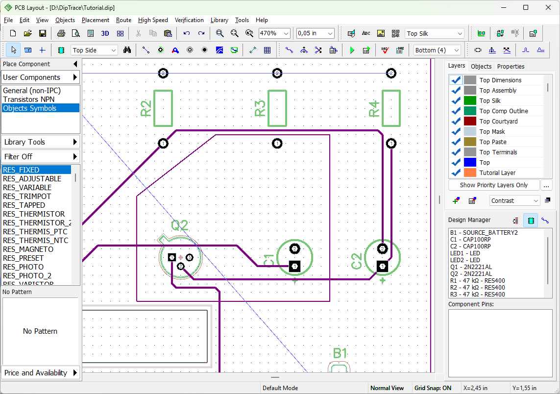
In the pop-up dialog box connect the second copper pour to Net 2, and specify the thermal type (4 Spoke should be fine). On the Pouring tab, set Line Width and Line Spacing to 0.004 in, and make sure the Unconnected checkbox in Island Removal is cleared. Press OK to close the dialog box and create a copper pour polygon.
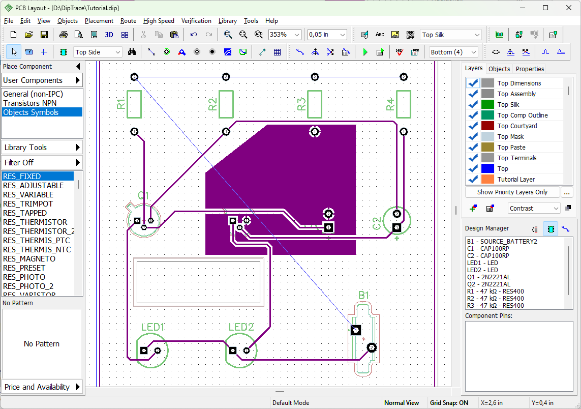
Now select Net 6 copper pour, which is unpoured now. Right-click on its border, and select "State / Poured" from the submenu. You will see that two copper pours connecting two different nets are independent and Net 6 copper changed according to the Net 2 polygon which has higher priority level.
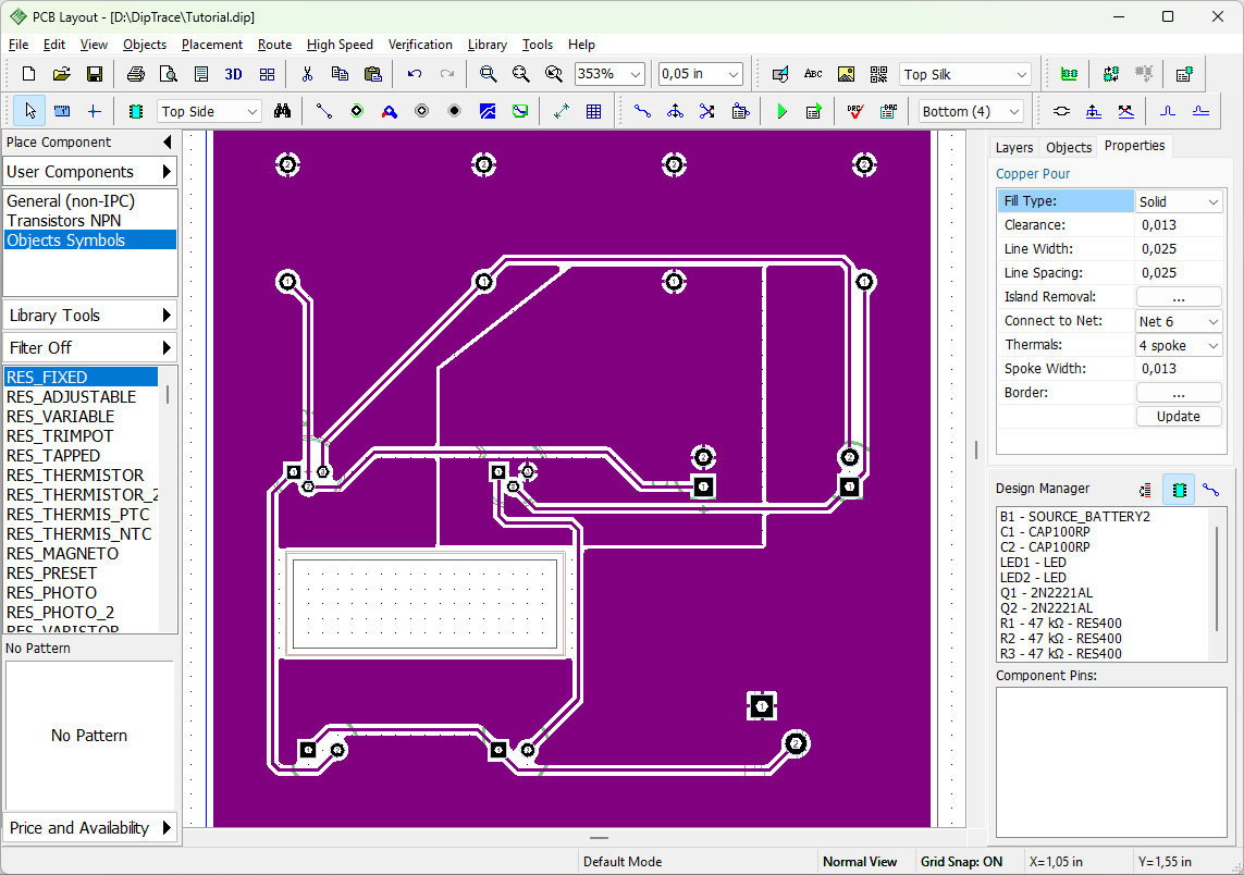
Thermals
Some pads require custom thermal connections that will be different from the copper pour's thermals. Right-click on a pad Q2:3 (when the pad is highlighted), and select Thermal Settings from the submenu, then check Use Custom Settings checkbox, and select a new thermal connection.
Some pads can become unconnected after placing a copper pour, because of selected thermal type and the layout structure (net connectivity check will report this), so selecting separate thermal settings for pads will help you to fix those issues.
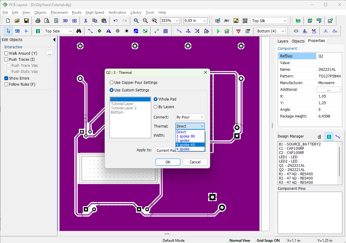
After changing thermal settings click OK to close the dialog box, then right-click on the copper pour border, and choose Update from the submenu to see these changes applied.
Select "Objects / Update All Copper Pours" from the main menu to update all copper pours at a time.
We'll try different thermals for pads to show you how it works.
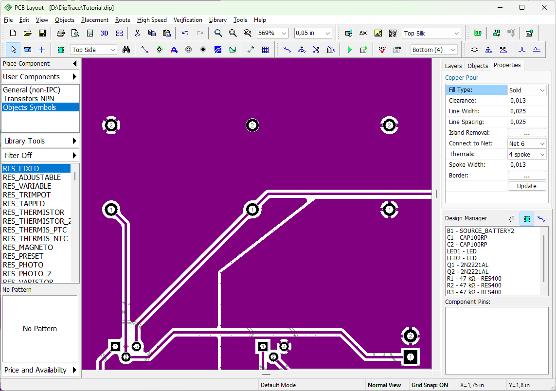
In the picture above, you can see that one pad has 4-Spoke 45-degrees thermal, another one is connected directly, and the third pad has 2-spoke 90-degrees thermal connection.
|
When the copper pours are used as Ground and Power planes, SMD vias usually connect to them by fanouts. You can create fanouts manually with the Fanout feature or automatically by Shape Router. |
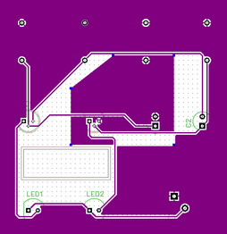
Let's see how to make a text etched in the copper pour. Switch to the Top layer, where we placed a text earlier. Right-click on the text object and open Properties dialog. In The pop-up select Type - Signal, Layer - Bottom and tick Invert Text box. Click OK.
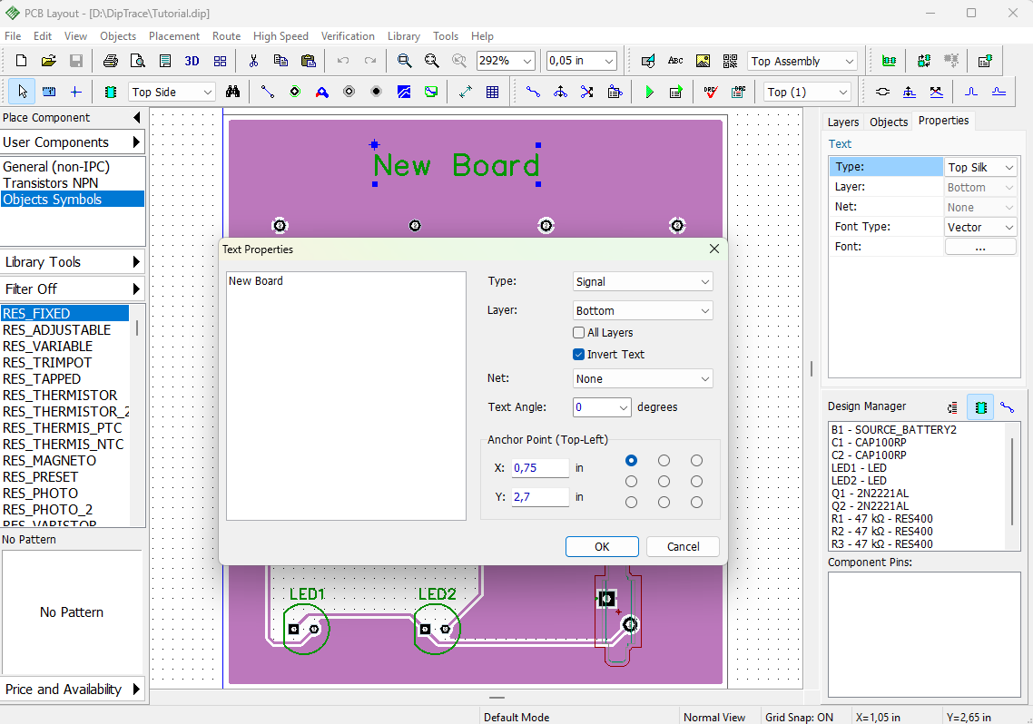
Now we'll have to switch to the Bottom layer and update the copper pour for the changes to take effect.You can see that the text has been placed as void in the copper and it's flipped (you can disable Flip Text Automatically option in the View menu for the text to be displayed without flipping on the Bottom Layer).
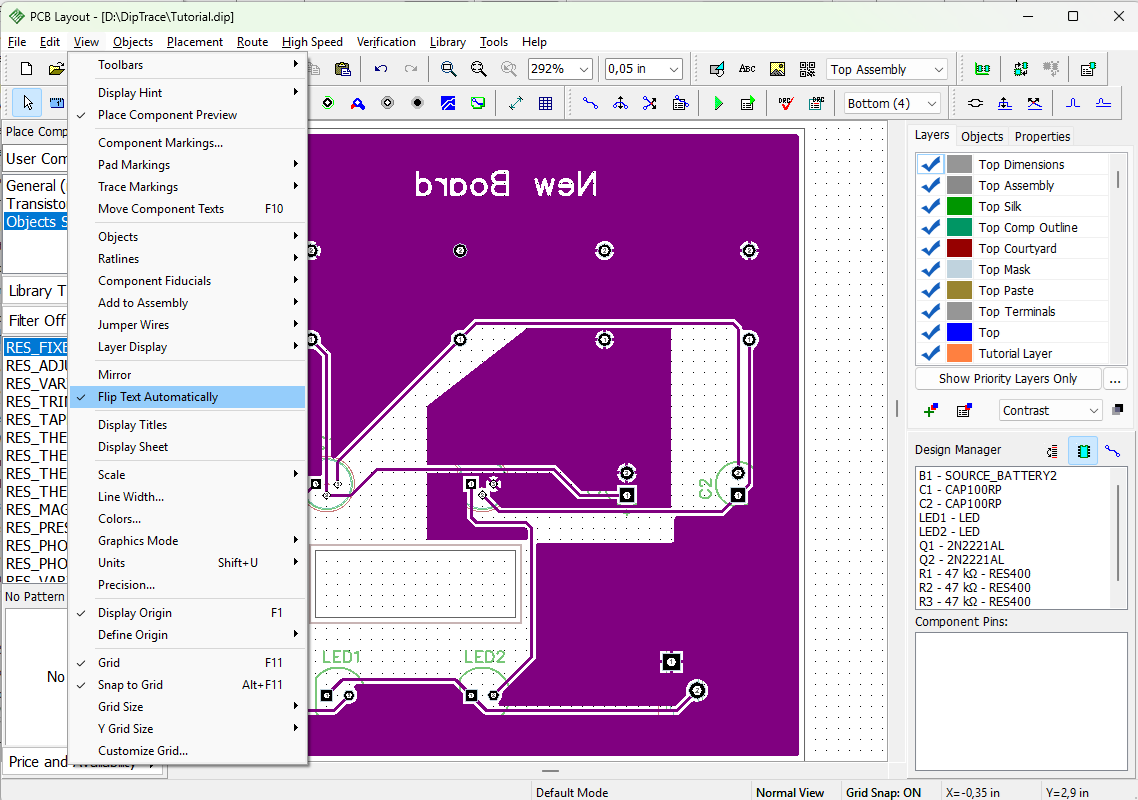
Undo the changes until the text is back in the Top Silk layer or just change the settings in the Text Properties dialog. Save the project.
19. Locking objects
Sometimes while making changes to the schematic or PCB, you need to lock some objects so you don't change them accidentally. Let's see how to do this in the DipTrace.
Switch to the Top layer, select several objects, right-click on one of them, and click Lock Selected from the submenu.
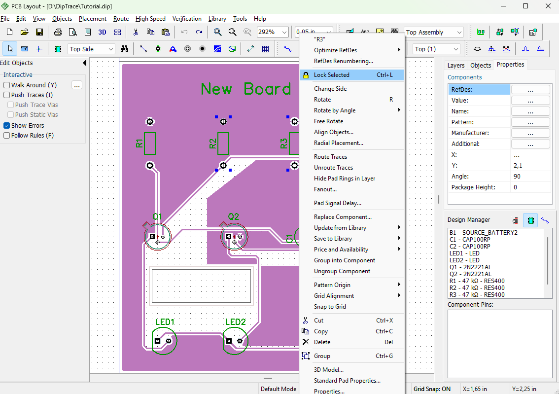
Notice that locked objects have their selection rectangles in lower contrast (in our case the color is similar to the copper pour, so we've made only current layer visible (with the drop-down list on the Layers panel or via the View / Layer Display menu). "Locked" text appears in the hint of the locked objects, you are unable to move, resize or edit them without unlocking first.
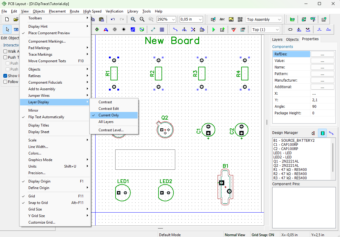
Now please unlock all objects, select all with Ctrl+A, and unlock ("Edit / Unlock Selected" from the main menu or Ctrl+Alt+L keyboard combination).
You can lock all the components after placing them on the top or bottom side of the board. Select "Edit / Lock Components / Top or Bottom" to lock the components on the respective layer (to unlock - just select the same item to disable it). Using this mode you can do the routing without worrying about changing something accidentally.
Return to the contrast layer display mode using the drop-down on the Layers tab (Design Manager).
Verification and output
20. Design verification
DipTrace has several verification procedures united in the Verification main menu item. We recommend using all three of them: DRC, Net Connectivity Check, and Compare PCB to Schematic.
DRC (Design Rules Check)
This feature is one of the most important verifications. It allows the user to check clearances between objects, control allowable object sizes, and differential pair parameters according to the set of design rules.
DRC works in regular (offline) and real-time modes. Real-time DRC checks all user's actions on the go. For example, when you move some component or create a new trace too close to another object, Real-time DRC shows red circles, which means that the clearance between these objects (trace, pad, copper pour) is smaller than the specified target value.
If the Real-time DRC function is not activated, you will not see errors until you start DRC manually in the regular mode by selecting "Verification / Check Design Rules" from the main menu or by pressing F9 hotkey. Error list or "No Errors Found" message will pop up. Most likely the current PCB has no errors because it is very simple.
Now select "Verification / Design Rules" to set up design constraints. There are four tabs in the pop-up dialog box: Clearances, Sizes, Real-time DRC, and Options.
Clearances. Specify object-to-object clearances. Uncheck All Layers item, select a layer from the list below, and define object-to-object clearances to be applied on a particular PCB layer.
Notice that clearance settings are NOT applied to nets with custom net class clearance (i.e. when Use Clearance in DRC option in Net Classes dialog box is checked) or Class-to-Class settings.
Check Same Net Clearance checkbox, and enter respective values, if you want to check the clearances between certain objects of the same net.
Sizes. Specify minimum and maximum allowed sizes for different elements on different layers.
Real-time DRC. Customize real-time DRC. You can turn it ON/OFF for specific actions, for example, manual routing, creating / editing, and moving objects. If you uncheck Enable Real-time DRC item, real-time verification will be turned OFF. However, enabling Show Errors option on the Routing panel will activate design rule check during manual routing, even if Enable Real-time DRC is unchecked - errors will be shown with red circles. Also, activated Follow Rules option will control that all design rules are followed and will not allow routing trace segments, if some violations are detected.
If you uncheck all secondary items in the corresponding tab, and leave only Enable Real-Time DRC item active, you will see errors right after completing a certain action, not while performing it. For example, if Moving objects item is checked, you will see errors before moving component to a new location, if this option is unchecked – you will see errors right after moving it, still no need to launch DRC separately. If Enable Real-Time DRC is unchecked, you will not see any errors (unless you enable Show Errors option for manual routing), till you start DRC manually.
Options. Set up other options.
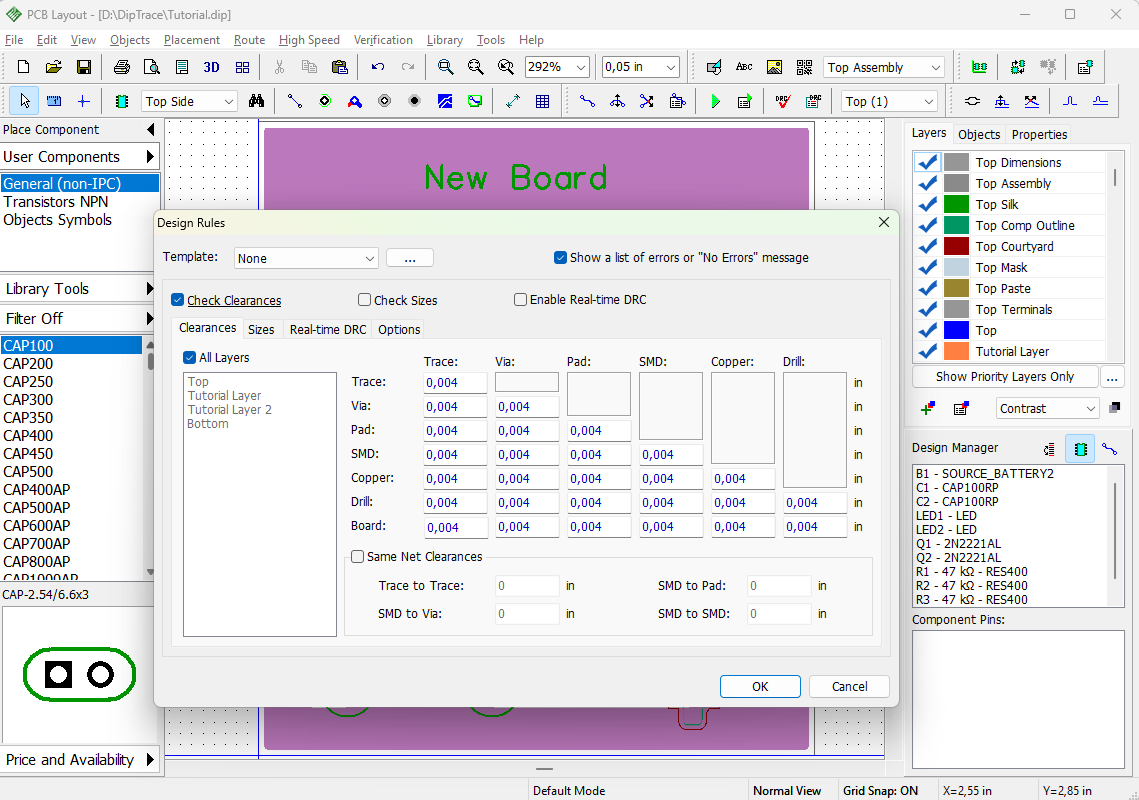
For this tutorial example, please turn OFF the size verification and Real-time DRC by unchecking the corresponding items. Make sure that Check clearances and Show a list of errors... checkboxes are checked. Keep settings like in the picture above (these values are quite small, but still within technical capabilities of most PCB houses).
Open the Options tab and make sure that Class-to-Class Rules, Length Matching, Copper Pours, or whatever objects you want to be verified are checked. Now let's try to see how DRC works in a regular mode. Even if the real-time DRC was ON during the design process, we recommend verifying project with regular-mode DRC at least once before exporting to Gerbers, just to make sure that everything is fine. Press OK to apply changes and close the dialog box.
Our project does not have errors, therefore we will create them intentionally. Select Bottom layer ("B" hotkey), switch OFF the grid (F11 hotkey), and move some trace until it touches the copper pour or another trace. Go to "Verification / Check Design Rules" or just press F9 hotkey to launch DRC. The list of errors will pop up automatically.
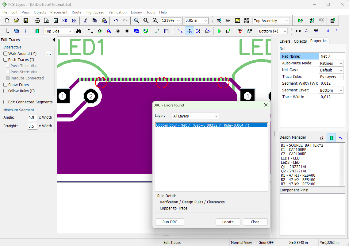
Errors can be sorted by layers. You can see the description of each error including the current value and the target value. Left click on the error in the list and DipTrace will show where to change the target constraint in the Rule Details section. Press Localize to see selected error on the design area and fix it. Red circle means a clearance error, magenta circle – size error.
Move the trace back to its original location without closing the error-report dialog, and then press Run DRC button. This time everything is OK and No Errors Found message appears.
Net connectivity check
This verification allows the user to check if all nets are properly connected. For such simple design this feature is not necessary, but if you have a larger board with many layers, pins, copper pours, and shapes, net connectivity verification becomes really useful. It checks the entire design and displays the list of broken and merged nets. Please select "Verification / Check Net Connectivity" from the main menu, and click OK in the pop-up dialog box. Most probably, your design will not have connectivity errors and you will see the No Errors message. More information about Net connectivity check.
Comparing to Schematic
This procedure allows you to check if PCB corresponds to the source Schematic file. Verification shows the net structure errors and unknown components. Select "Verification / Compare to Schematic" from the main menu then choose source Schematic file, and press OK. If your net structure was not changed and has no errors, you will see the "No Errors Found" message, otherwise, the list of errors will pop up.
Net connectivity check and Comparing to Schematic features work fast and provide an easy-to-understand user interface with reliable functionality.
21. Layout information
What about counting the number of pins or the board area? Select "File / Layout Information" from the main menu in the PCB Layout module.
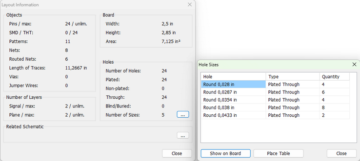
Here you can preview the number of different objects, layers, board and hole sizes. Press button in the Holes section to open the Hole Sizes dialog box. Press Show on Board button to highlight holes by size directly on the design area.
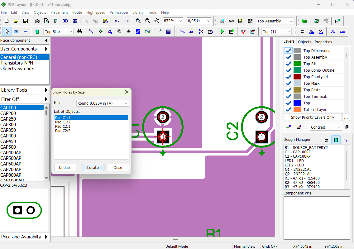
Close the dialog box, and save the layout.
22. Panelizing
With DipTrace you can panelize similar or different boards on a single layout.
Panelize project
If you need several copies of the same PCB, select "Tools / Panelizing" from the main menu or press  button on the Standard toolbar.
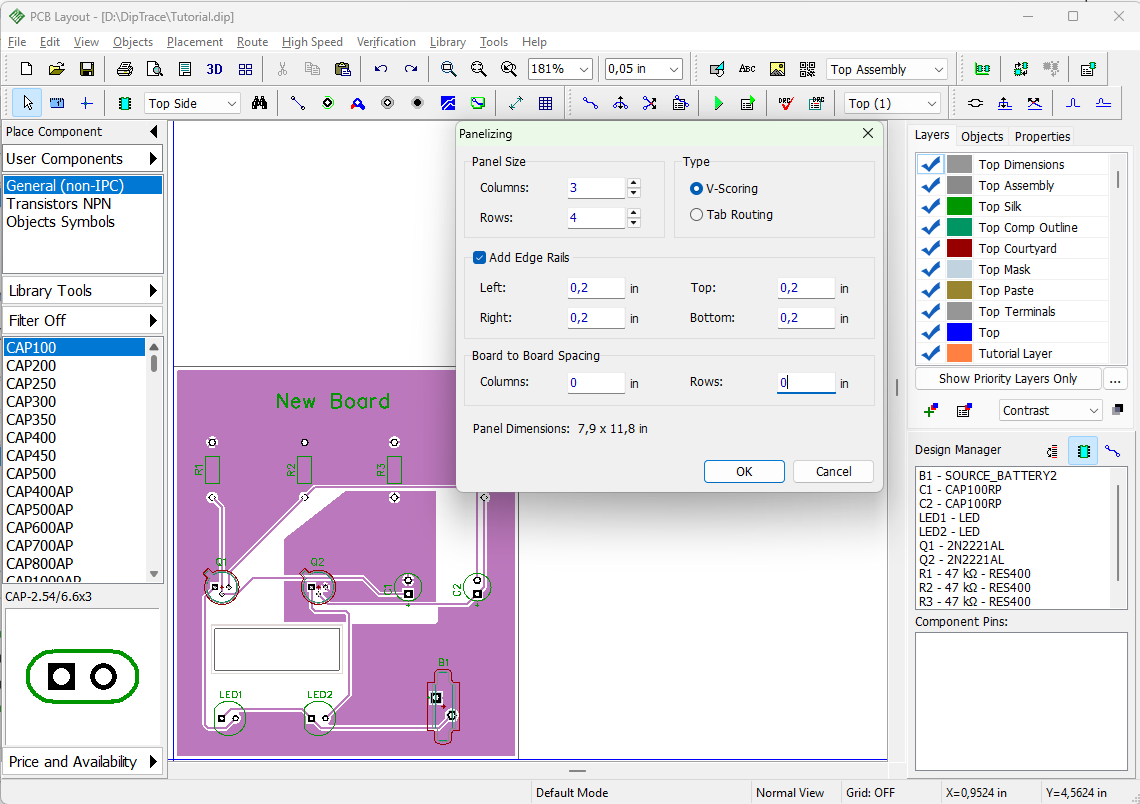
We will make 12 copies of this circuit board, 3 columns and 4 rows. Since our board is of a regular shape and does not have any parts overlapping the edge, we will use V-Scoring to facilitate the panel break-off. “Board to Board Spacing" will be zero (however, always check the requirements of your manufacturer).Tick Add Edge Rail checkbox and enter 0.2 in for each side to add a frame along the perimeter of the panel and make sure it’s suitable for industrial assembly. Click OK.
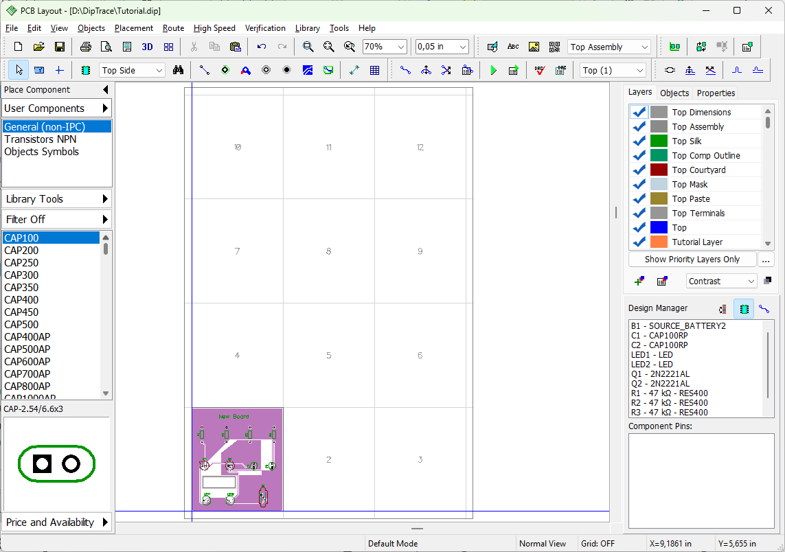
We can see only boxes with "#" text on the design area, but you can check the final layout in the Print Preview dialog box ("File / Preview" from the main menu), while printing or exporting to manufacturing formats.
It is possible to exclude some objects from panelizing (for example, holes or shapes). To exclude any object from panelization, right-click it, and check Do Not Panelize. This item is available only if Panelizing is active.
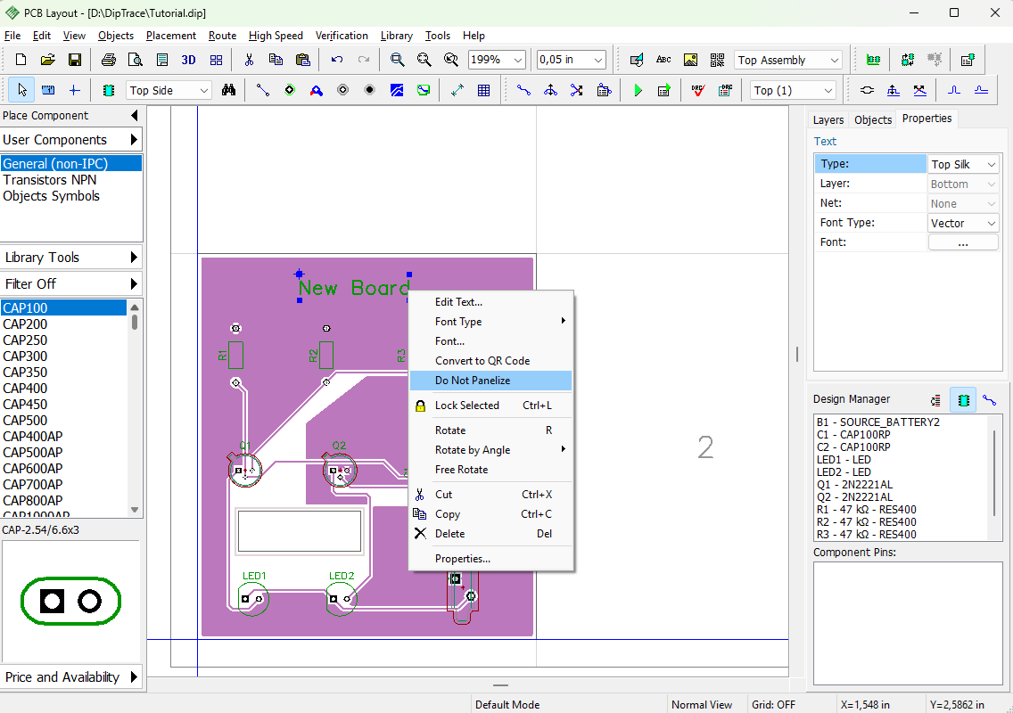
Notice that panelizing works only if PCB has a board outline.
For more details about panelization for Tab-Routing panels as well as V-Scoring and Tab-Routing combined, please consult PCB Layout Help.
Now open the Panelizing dialog box and change the number of columns and rows to "1" to remove copies and let us practice with panelizing different boards on a single layout.
Panelize different projects
Check "Edit / Keep RefDes while Pasting" item from the main menu, then select all objects (Ctrl+A) of your layout, and press Ctrl+C to copy them, then right-click on an empty spot on the design area (this will be an upper-left corner of the second board), and select Paste from the submenu.
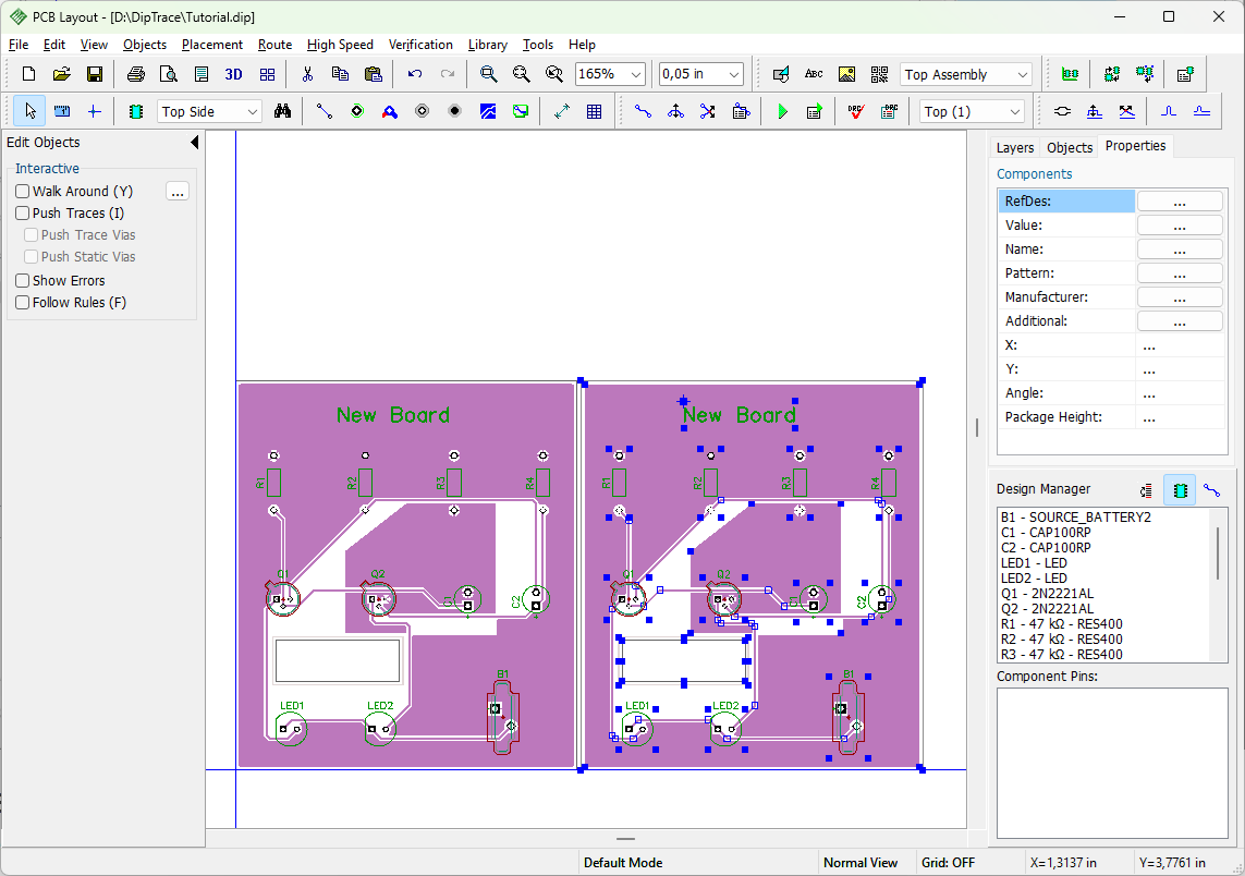
We got the second copy of our PCB (but it can be a different PCB, if you want). Reference designators will not change.
Notice that you need to create a common board outline and board cutouts; additionally, non-signal layers may be required for correct manufacturing. More information at our YouTube channel.
If Keep RefDes while Pasting item is checked, pin limitation of your DipTrace edition (Free, Lite, Standard, Extended) does not apply, so you can easily panelize several 300 pin layouts even with DipTrace Freeware.
23. Printing
We recommend using the Print Preview dialog box to print PCBs, select "File / Preview" from the main menu or press  button on the Standard toolbar. Notice that we did not describe creating titles in the Designing a PCB section of this tutorial. If you want to display titles, select "File / Titles and Sheet" from the main menu, and select ANSI A in the Sheet Template drop-down list, then check Display Titles, and close the dialog box before opening the Print Preview dialog box.
More detailed information about Titles and Sheets as well as creating and editing titles with the Title Block Editor in the DipTrace Help ("Help / PCB Layout Help" from the main menu).
Use Print Scale drop-down list or Zoom In / Zoom Out buttons to change the scale of the layout on the sheet and press  button to move design on the sheet.
In the upper-left, you can select current Signal/Plane layer and layer display mode. If you want to get a mirrored PCB or text, check Mirror or Flip Text checkboxes (the Flip Text box is disabled if "View / Flip Text Automatically" main menu option is ON).
Press Print button to print the layout. Press Save Picture if you want to save an image to PNG, BMP or JPEG file or press Export PDF if you want to export to PDF. The small button with colors to the left from the "Zoom Out" tool allows the user to define print colors ("View / Colors.../ Print Colors" from the main menu).
Notice that only layers with default color depend on the color scheme.
For printing all in black and white without changing layer colors, check Print in Black only box.
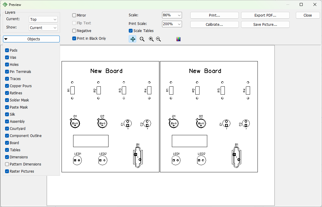
For hobbyist's attention. Be aware that laser printers often introduce some degree of dimensional distortion due to heat expansion of the paper. It depends on your laser printer and the quality of the paper used. For most people, it's not important. However, one way to cope with this issue is to preheat paper by running it through the printer, without printing on it (for example, you can print just a dot in the corner). For ink-jet printers, this is not an issue since ink-jet technology does not heat paper. Laser printers do not always visibly distort images but you have to be ready that this can happen. You can use the Calibration feature in the Print Preview dialog box to minimize heat distortions.
There are two methods of prototyping a PCB at home: using a TT (Toner Transfer) or UV exposure. TT is definitely a method for a laser printer, and UV exposure is better with ink-jet printers.
Close the Print Preview dialog box and Undo several times to remove the second PCB and return the board without panelization. Then save the layout.
Generating files for manufacturing
Manufacturing file formats and ordering
24. DXF
DXF output allows for exporting data to many CAD / CAM programs which support DXF import (AutoCAD and others).
DXF export
To export the circuit board to DXF format, select "File / Export / DXF" from the main menu, select layer from the list of all layers, and check/uncheck the corresponding boxes to show/hide different objects on this layer (text, pictures, vias, etc.). Set up the offset (distance between zero and the bottom-left corner of the board: design origin or custom value), mask and paste layers if needed. You can save each layer into a separate DXF file, but in order to export entire board into a single multi-layer DXF, press Select All button.
Notice that "Edge_Top" and "Edge_Bottom" are not selected. Technically these are not the physical layers of your circuit board. They are exported only if you are going to manufacture the board using milling method.
Press Export button, specify the name of the file, location, and save the circuit board into a DXF file.
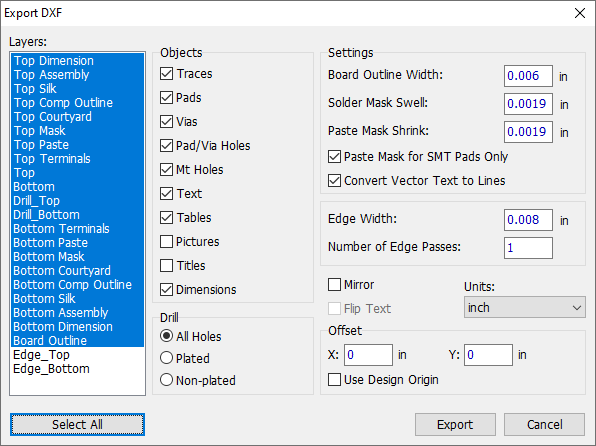
All layers of the board will be exported into a single DXF file. You can open it with AutoCAD or another program that reads AutoCAD DXF.
Export for milling (DXF and G-Code)
Milling method is convenient and cheap for non-complex boards.
Notice that copper pours (unlike thermals) are not considered when exporting edges for milling.
Select "File/ Export/ DXF" to open the DXF Export dialog box, then select Edge_Bottom layer, because all traces of our PCB are on the Bottom layer (if you have traces in the top layer, select Edge_top), check Mirror checkbox to mirror the design (for the bottom layer). This will allow us to see the actual bottom side of the board. You can leave default values if you're not familiar with specific milling settings or define the Edge Width parameter. Center line of the milling will be calculated as a half of the Edge Width value. Milling depth depends on the edge width and the instrument angle.
Press Export button, and save the DXF file.
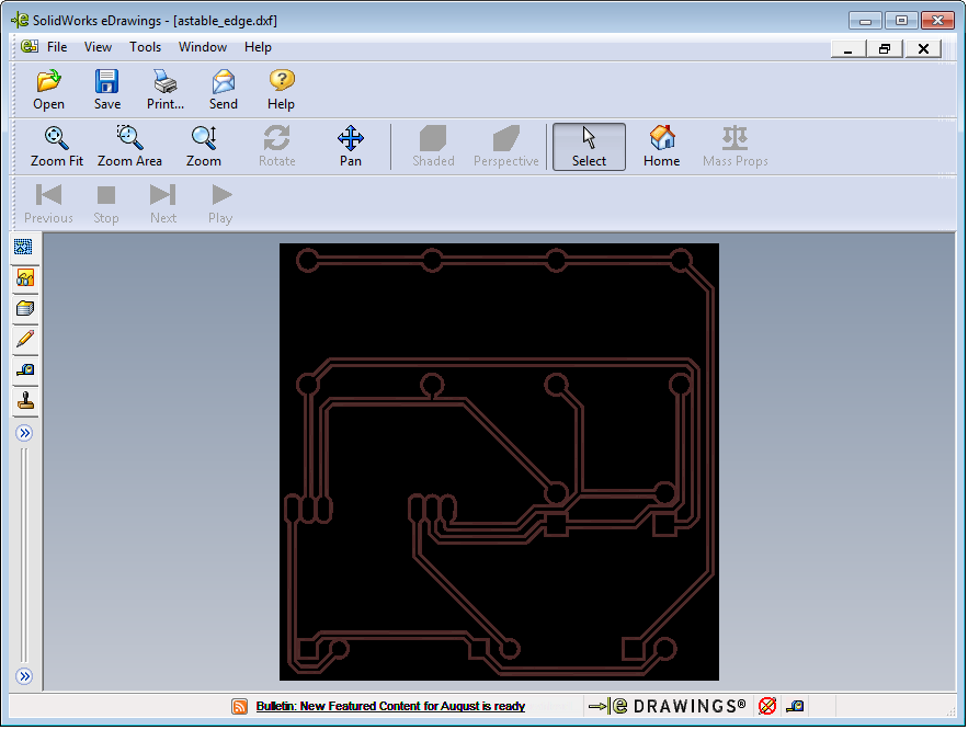
The edge exported from the DipTrace is a set of polylines with defined width. DipTrace checks design before export and if object-to-object clearances are less than the edge width, DipTrace shows a warning message and enables the designer to correct errors.
Notice that CAD programs usually show polylines with sharp angles, but when you mill the board or simulate milling with a CAM program, everything will look rounded because of the instrument radius.
CNC drilling machines work with G-Code files. Convert your edge from the DXF format to G-Code, using ACE converter, FlatCAM (both are free) or another software.
Please Undo several times to return the copper pour if you deleted one.
25. Gerber RS-274X
DipTrace allows the user to export a circuit board to Gerber format, accepted by almost all PCB manufacturers around the world.
Select "File / Export / Gerber..." from the main menu. In the Export Gerber dialog box select a layer from the list (multiple selection - Ctrl or Shift) and use the corresponding check boxes in the Objects section to specify, which objects will be exported to Gerber.
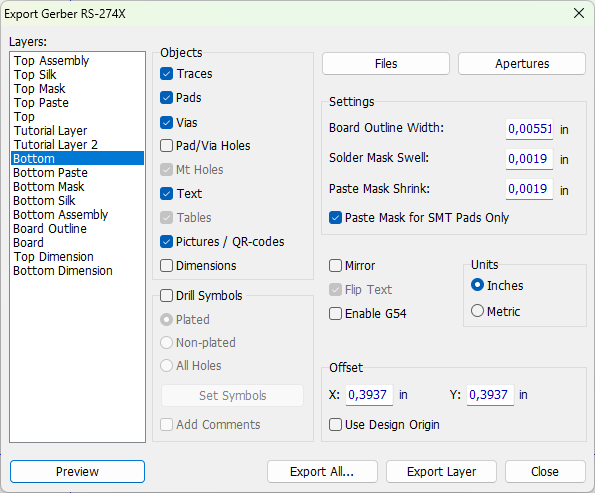
Press the Preview button to preview the selected layer. Unlike DXF, all layers should be exported to Gerber format separately, one layer per file. The image below shows the bottom layer of our PCB in the Gerber preview dialog box. You can zoom in and out. Press Close button to close the preview dialog box.
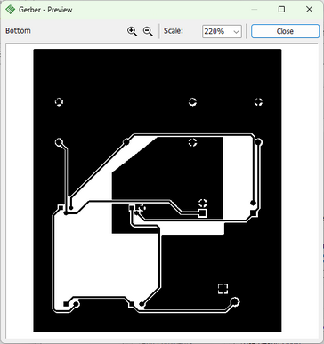
Press Export All and DipTrace will offer you several options to generate output files: zip archive with Gerber files only, zip archive with Gerber files and NC Drill (remember that PCB houses need Gerber and N/C Drill files to manufacture your PCB) or files for each layer separately. Once you export those, you can send them out for manufacturing.
Gerber layers
1. Top Assembly – this is assembly layer, it includes all shapes/texts placed on the Top Assembly as well as objects defined in the "View / Add to Assembly" main menu item.
2. Top Silk – includes pattern shapes, texts and all other shapes and texts placed in the Top Silk layer. Do not change these settings, and press Preview. Notice that if you use the TrueType fonts, some parts of the text can be invisible (depends on the font and size).
3. Top Mask – this is a solder mask layer. It is generated automatically, based on pads, custom pad settings, and common Solder Mask Swell parameter, defined in the Export Gerber dialog box. This layer also includes shapes placed in the solder mask layer. We should uncheck the Vias box (exclude vias from the export) because vias are usually covered with the solder mask. To change custom solder mask settings for pads, right-click on the pad, and select Mask / Paste Settings from the submenu.
4. Top Paste – this layer is used for SMD pads only, so we can check Paste Mask for SMD Pads only.
5. Signal layers (Top, Bottom, etc.) – these are copper layers. Please check the Vias checkbox for all of them and preview each one to make sure that layers are correct.
Notice that Pad/Via Holes item in the Objects section should be checked only if you plan to drill holes manually (not using a PCB house). If Pad/Via Holes check box is checked, two Gerber layers will be created inside one Gerber file: Positive Drawing and Hole Clearing. The second layer is used to remove artifacts over the drill holes. Manufacturers prefer Gerber files without pad/via holes.
6. Bottom Paste, Mask, Silk and Assembly layers are just like their analogs from the top side. By default all text objects in Bottom layers are flipped – "View / Flip Text Automatically" option from the main menu.
7. Board Outline layer includes the outline of the board or panel, if the board is panelized.
8. V-Scoring - contains V-scoring pattern, if this type of panelization is used for the design.
9. Board layer includes the board as a filled polygon.
10. Top/Bottom Dimensions – layers created specially for dimensions. These layers are blank in our case because the current project does not have any dimensions on the design area. Top / Bottom Dimensions can help some manufacturers to avoid mistakes in sizes.
Notice that NOT all layers are necessary for successful board manufacturing. It depends on your project and additional features that you order.
Other settings
The Offset parameter in DXF, Gerber, N/C drill, and Pick and Place export dialog boxes is the distance between the zero and the bottom-left corner of the board. You can use a custom value or design origin (check the corresponding item or enter values in the Offset section of the Gerber export dialog box).
Press Files button in the upper-right corner of the Export Gerber dialog box, define filename and extension for each Gerber layer, and include or exclude certain layer/s from exporting when you press the Export All button. Select a layer in the list, and type in a new name and extension. Layer name and project name tags are supported. You can also adjust how to export NC Drill files in Export All Options section; those settings will be applied if you chose to export both Gerber and NC Drill files together in one archive. We will not change anything, keep the <layer> tag – all files will be named as layers. Press OK.
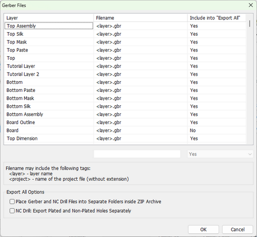
Drill Symbols (Legend)
Some PCB houses require Drill Symbols. DipTrace allows you to export them as a separate Gerber file. Check the Drill Symbols checkbox in the Export Gerber dialog box, then press Set Symbols button. In the pop-up dialog box, you need to manually assign each hole with the symbol from the list in the right side or press the Auto button to assign all symbols automatically. Close this dialog box.
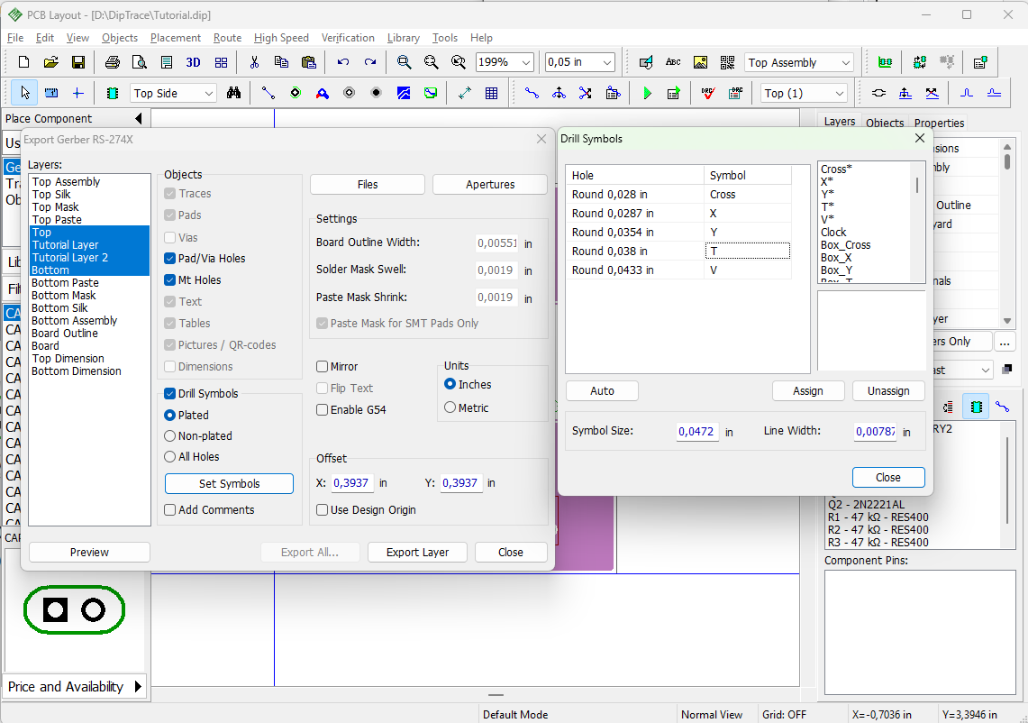
Now check the Add Comments checkbox, and press Preview. You will see the drill symbols and a table with hole parameters.
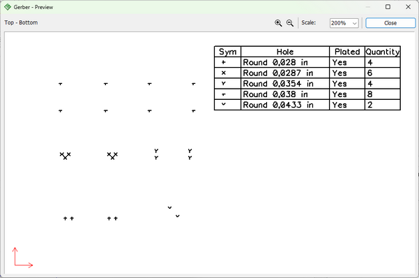
Close the preview panel, and press Export layer to save Drill Symbols in the file. Drill symbols will be exported in a separate file just like any other Gerber layer. If apertures are not defined, DipTrace will ask you to set them automatically.
Uncheck the Drill Symbols checkbox when done, otherwise, you will get a blank file/preview while exporting silk, assembly, signal layers, etc.
DipTrace allows the user to export any texts, fonts, and Unicode symbols (even Chinese hieroglyphs) as well as images (company logo, etc.) to Gerber format. All those objects are vectorized.
We recommend checking Gerber files with third-party viewer, before sending them for manufacturing. The best option is to use the same software (or a free viewer) as your board manufacturer, because some programs may read Gerber files a bit differently from the official RS-274X specification.
We tried to take into account specifics of different manufacturing software in DipTrace Gerber export feature, but verifying files is a very good practice.
If you don't know what software your manufacturer uses, we recommend Pentalogix Viewmate, it has strict RS-274X conformity.Or in the Ucamco online Gerber viewer..
26. Gerber X2
Gerber X2 is the latest evolution of the Gerber format and DipTrace was one of the first electronic CAD systems with Gerber X2 support. If your PCB manufacturer accepts Gerber X2 files, you can completely enjoy the benefits that format gives to an engineer. Gerber X2 stores information about PCB stackup order, a function of each layer, PCB attributes and pad functionality.
Select "File / Export / Gerber X2" from the main menu in the PCB Layout. Since Gerber X2 is compatible with Gerber RS-274X, the dialog boxes are identical and exporting procedures do not differ from the ones described in the Gerber Output topic of this tutorial.
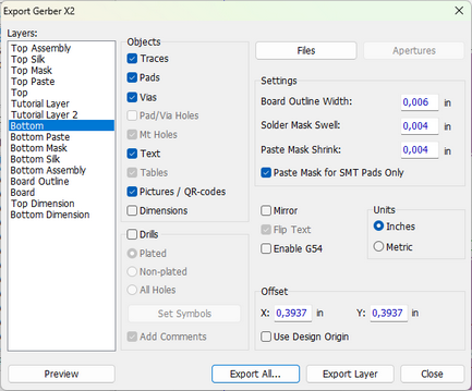
However, Gerber X2 saves comprehensive drill layout in the Gerber-formatted file (not just Drill Symbols, like Gerber RS-274X). To export drills, check Drills checkbox, select all copper layers (they should be selected by default) to export through holes, then press Export All button and select one of the options - Zip Archive: Gerber X2 or All Files Separately - to export all holes of the project automatically into the corresponding Gerber file/s. Each type of the hole goes into a separate Gerber Drill file. Note, however, that most manufacturers still require drills in the N/C Excellon format. You can export both Gerber X2 and NC Drill files simultaneously - press Export All button and select the respective option.
Check with your PCB house if it accepts Gerber X2.
27. N/C Drill file (Excellon)
If you order board manufacturing at a PCB house, you need to provide Gerber and N/C Drill files. Select "File / Export /N/C Drill" from the main menu, then press the Auto button to define the tools. Press Files button, if you want to configure default names of NC Drill files. Hit Export All button to save all necessary files automatically. Use the Preview button to visually check the layout.
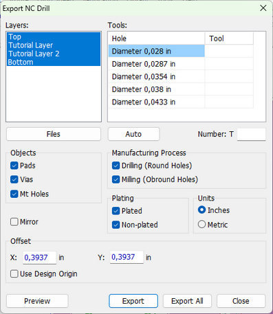
If you want to export just the holes of a certain type separately from the other, select the layer pair of the via style, and press Export.
Remember that you can also export both Gerber and NC Drill files in one click in the Gerber export dialog.
Notice that for through holes all layers should be selected, for Blind/Buried vias – only top and bottom layers involved in the via style.
28. ODB++
DipTrace allows the user to export circuit boards into ODB++ format for manufacturing. Select "File / Export / ODB++" from the main menu in the PCB Layout. In the pop-up dialog box you can check or uncheck certain PCB layers for exporting, change default solder mask swell and paste mask parameters with respective fields and checkboxes, edit the offset values. The export mode can be defined by choosing between CAM350 and Mentor Graphics ODB++. For Mentor Graphics option, ODB++ 8.1 version is available. Default settings usually work for most cases so do not change them unless it's really needed.
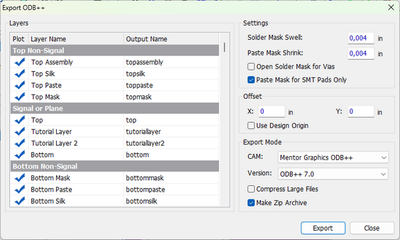
If Make Zip Archive item is checked, DipTrace will zip all ODB++ files into a single file for sending out to the board manufacturer. Press Export and specify a folder, where you'd like to save the output files. You can preview ODB++ files with a free Mentor Graphics ODB++ Viewer.
29. Order PCB
For those who doesn't want to look for a PCB house to manufacture a circuit board, DipTrace allows for a simple ordering tool with Bay Area Circuits, our partner PCB manufacturer in California. No need to export Gerber or N/C Drill files, enter a few details and manufactured board will be delivered to your place. Go to "File / Order PCB" from the main menu in DipTrace PCB Layout, select "Bay Area Circuits" from the Manufacturer dropdown list, review the board parameters, specify quantity, manufacturing time, shipping address, name, phone, email, and some additional details. The price will be calculated automatically.
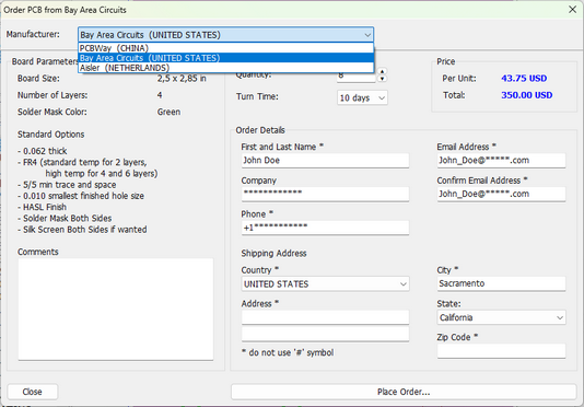
Press Place Order button to open the order page in your web browser, review the total cost, including shipping. Online payment is done via PayPal.
DRC checks your PCB automatically. If there are errors, we recommend to carefully review and fix them. Please do not allow for any ambiguity, especially related to Solder Mask and Solder Paste settings. Describe it in the Comments section, or contact Bay Area Circuits to clarify any of the questions that you think may arise.
Email: support@bacircuits.com
855-811-1975 FREE (toll free)
510-933-9000 (local)
510-933-9001 (fax)
Corporate Headquarters
44358 Old Warm Springs Blvd
Fremont, CA 94538
DipTrace can also generate all the necessary files for ordering PCB manufacturing from PCBWay (China) or Aisler (Netherlands). To do this, select the desired manufacturer from the Manufacturer dropdown list and click "Place Order." The software will automatically create an archive containing all necessary files and open the manufacturer’s order page, where you can complete the order.
Congratulations! You have finished designing a simple project with DipTrace.
Please, save your schematic and PCB files if you want.
P.S. Do not forget to uncheck the Use Priority Layer Directions check box in the Autorouter Setup dialog box if you plan to route 2+ layer boards.
Creating pattern libraries
30. Creating Component Libraries
In this part of the tutorial we will show how to create component and pattern libraries. In most cases you can find appropriate pattern in DipTrace standard libraries and attach it to a new component, but for demonstration purposes we will create a new pattern from scratch.
Important:
In this tutorial we often refer to components as patterns or footprints (if talking about the PCB Layout), while in the Schematic components are often called symbols, component symbols, or schematic symbols, all these mean the same physical electronic component.
A regular component in DipTrace consists of a schematic symbol, a pattern drawing and, possibly, a 3D model. All three represent the same entity, but on different stages of the design: schematic capture, PCB Layout, and 3D visualization/export respectively.
Components and attached patterns are saved together in the files with *.eli / *.elixml extension. Components are always stored in libraries. If if you need to create just a single component, you have to create a separate library for it or ad it to an existing user library.
DipTrace also allows access to patterns separately from the components. Patterns are also stored in libraries. Pattern libraries are saved with *.lib / *.libxml extension. No surprise, these files are only accessible in the PCB Layout and Pattern Editor.
*.wrl, *.3ds, *.iges, and *.step files store 3D models. Patterns and schematic symbols can exist as separate stand-alone parts, but correct component always have all of them properly connected.
Different schematic symbols can have the same pattern (footprint) attached to each of them and vice versa, for example the same resistor can be in through-hole and SMD packages.
DipTrace has two separate programs Component Editor and Pattern Editor for designing components. Component Editor is used to manage components – draw schematic symbol and connect them with pattern drawings (footprints). However, pattern drawing is not editable in the Component Editor, Pattern Editor should be used instead.
Read Working with libraries topic in the Component and Pattern Editor Help documents for more details.
31. Designing a pattern library
Open DipTrace Pattern Editor, i.e. go to "Start / All Programs / DipTrace / Pattern Editor" on Windows machine or use DipTrace Launcher on MacOS.
If you create a new component it is always better to start with drawing a PCB footprint (pattern), which you can assign to a certain schematic symbol in the Component Editor. If you know that the pattern is already available in the standard pattern libraries, you can proceed directly to the Component Editor to draw the schematic symbol, attach that existing pattern, and save complete component in the component library (*.eli / .elixml file). However, we will start from the footprint design just to show you, how to do that and give you a full perspective of the design process.
There are two ways to create patterns - manually and automatically (using Pattern Generator). We will go through both methods of creation of patterns for a through-hole and a surface-mount device.
32. Customizing Pattern Editor
First of all, we need to show a center point and X, Y-axes, select "View / Display Origin" from the main menu or press F1 hotkey (if it is not displayed yet). Notice that you can change the origin at any time while designing a pattern ("View / Define Origin / ..." from the main menu or press  button on the Instruments toolbar). Origin is a zero point of the pattern when you place, rotate, or change pattern's position by coordinates in the PCB Layout.
You can configure the precision level by defining the number of decimal places (up to ten) for all the values used in the project by units and set the minimum grid size and grid precision for the current units, using Precision of Values dialogue-box ("View / Precision…").
Please note that high precision rates are used only at designing stage. When the project is saved into a file, precision up to 0.001 mil is applied.
Pattern Properties panel in the upper-left of the design area allows the engineer to design patterns by types or templates, define pattern attributes, attach 3D model, and change default pad settings. The panel can be hidden, minimized or moved during pattern design. To minimize the panel, click the arrow button in its upper-left corner. To expand the panel, left-click on its border and drag it.To hide/show this panel select "View / Toolbars / Pattern Properties" from the main menu.
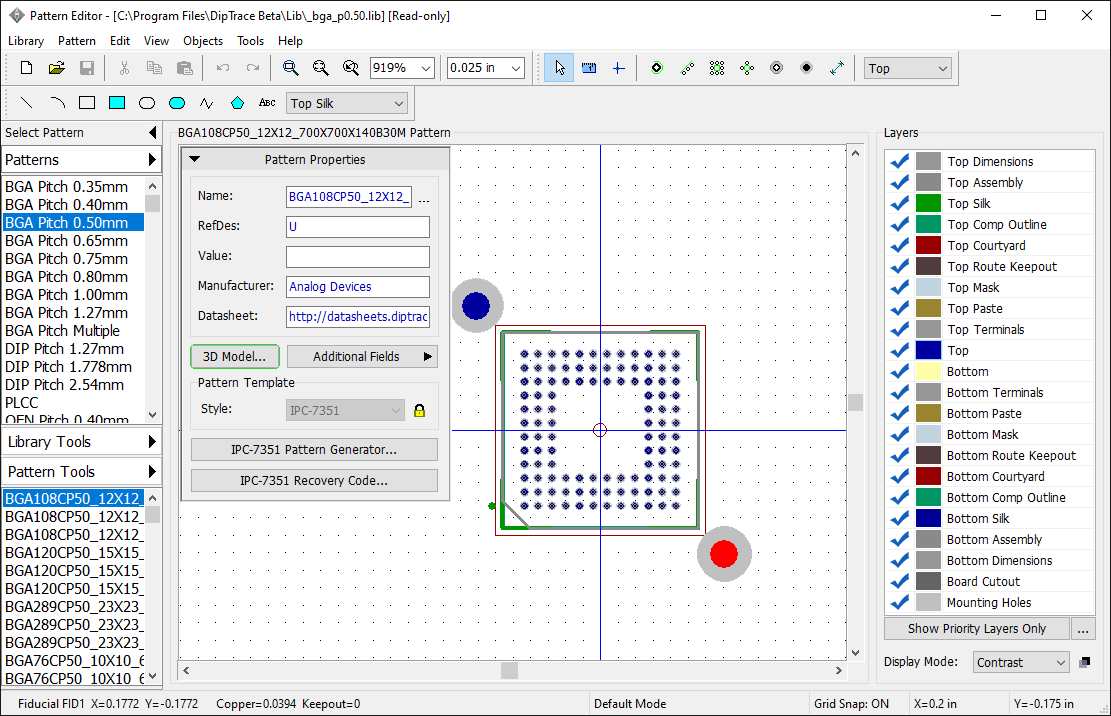
Use the Plus Sign (+) and Minus Sign (-) hotkeys or the mouse wheel for zooming in and out in the Component and Pattern Editors or change scale in the scale box on the Instruments toolbar. Go to "View / Pad Numbers /..." to show/hide the pad numbers.
You can also choose to display a standard or detailed hint (with pad/hole dimensions) for the objects on the design area ("View/ Display Hint").
Notice that hint is also shown in the bottom-left corner of the screen.
33. Create/Save library
Create a library
Press  / New Library on the Library Manager panel on the left side of the screen. In the pop-up dialog box enter the library name, hint, and select the library group. You can't save a library outside any of the library groups. We recommend creating new libraries in the User Patterns library group offered by default. Press OK.
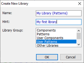
A name of your library will appear on the Library Manager panel, User Patterns library group becomes selected automatically. Now save the newly created library in a separate file.
Save library
|
Once a library has been created you need to save it in the file. Select "Library / Save" from the main menu. We recommend saving user libraries in the "Documents/DipTrace/My Libraries" folder for Windows, which is offered by default, however, you can select another location (Mac users should save custom libraries in another location because you can accidentally lose the "My Libraries" folder when uninstalling the software).
|
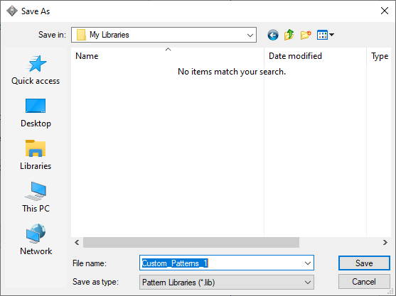
DipTrace does not allow saving user libraries in the folder with standard libraries.
You can save the library in XML format if version control is required.
Type in the file name (not shown in DipTrace), and press Save.
Now we have "My Library (Patterns)" pattern library saved on your computer. Notice that file has *.lib or *.libxml extension, meaning that this is a pattern library.
Designing a resistor pattern
34. Designing a resistor (pattern)
We will design the first pattern of our library, it is going to be a resistor with 400 mils lead spacing. First, let's see, how to create it manually and then move on to the automatic generation of the pattern.
35. Manually
To start, we'll have to name the pattern and fill in the basic description fields. Type "RES 400" into the Name field, "R" – into the RefDes field and "47kΩ" – into the Value field on the Pattern Properties panel. In DipTrace Pattern and Component Editors, you need to define just a basic RefDes (not a number index). For example, when you place several resistors: R1, R2, R3, etc., the designators will be assigned automatically. Use Windows Special Characters Map to find and copy/paste special symbols for Ohms, Farads etc.
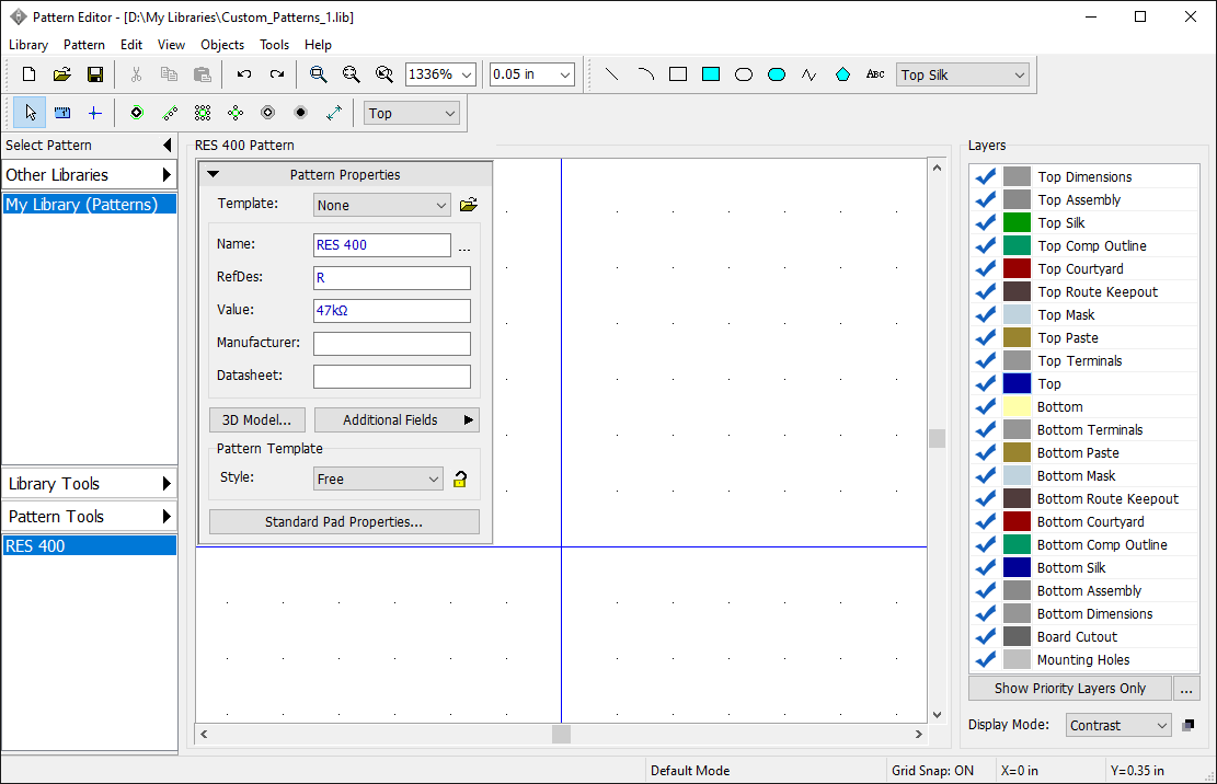
For this pattern, we have used the Free style, but it is faster to use Lines instead. You'll see how to use this option in one of the subsequent topics.
Placing pads
Please make sure that 0.05-inch grid is selected (change measurement units in the "View / Units" main menu item or with Shift+U hotkeys) then minimize the Pattern Properties panel. For convenience, you can activate Snap to Grid option in View menu. Select the Place Pad tool ( button on the Objects toolbar) and left-click on the design area to place two pads like in the picture below. Right-click to exit placement mode.
Note: for through-hole pads Pattern Editor applies color settings defined in PCB ("View/ Colors"), that's why they are colored black in our case instead of blue.
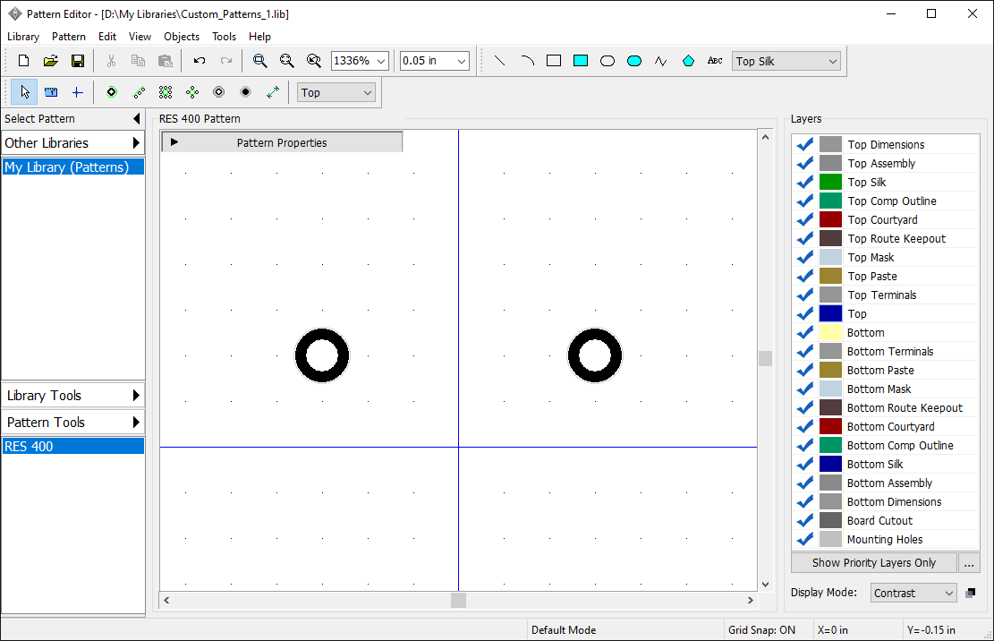
Let's place a dimension line, this will make editing more simple and visual. Select "Objects / Place Dimension / Horizontal" from the main menu or Place Dimension / Horizontal tool on the Objects toolbar, left-click in the center of the first pad, then in the center of the second pad, move the mouse pointer a bit upwards, and click one more time to place a dimension line. The key points of the object are highlighted when you hover over them with your mouse. Dimension pointer is attached to the key point, it recounts parameters automatically, when you move or resize objects.
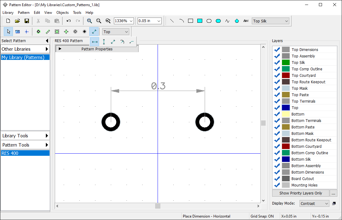
Right-click on the dimension line, and select Properties from the submenu if you want to change Layer, Units, Arrow Size etc. Drag and drop the dimension line like a regular object if needed.
Move the pads so that the spacing between them is 0.4 inches.
Layers
On the right side of the screen, there is a layer list. All signal and non-signal layers of the pattern are displayed here. The panel facilitates layer management: you can show/hide a layer on the design area by clicking on the corresponding blue check mark, change layer color (a left-click on the color rectangle) and quickly select the layer for object placement.
Let's short list the layers, press  button below the list of layers. In the pop-up, select Top Dimensions, Top Silk, Top Comp Outline, Top Mask, Top Paste, Top, Bottom layers in the Priority column. You can change the position of the layers in the list by using arrow buttons in the Order column, but we'll leave the order of layers as it is. Click OK to close the dialog. Pres Show Priority Layers Only to display only previously selected layers in the list.
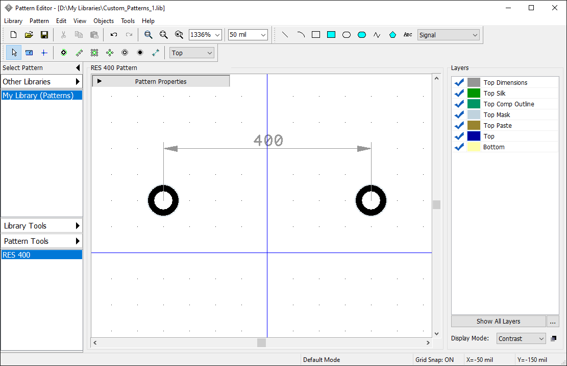
Pad properties
|
Pads can have default or custom properties. Default are applied to all pads of the pattern, custom – only to selected pad/s. To change default pad settings, select "Pattern / Standard Pad Properties" from the main menu or press Standard Pad Properties button on the Pattern Properties panel. In the pop-up dialog box, you can change the pad shape: Ellipse, Obround, Rectangle, D-Shape or Polygon (click Points for polygonal pad customization). Corner Radius can be defined for Rectangle pads. You can make round or obround holes and change the hole diameter (for Through pads only). |
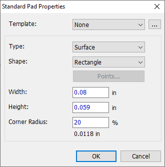
Pad templates allow the user to quickly apply selected parameters in different dialog boxes of the Pattern Editor and PCB Layout.
Change pad Type to Surface, shape to Rectangle, width to 0.08, height to 0.059, and corner radius - 20%, then click OK to apply changes. You can also change the measurement units (mil is 1/1000 inches).
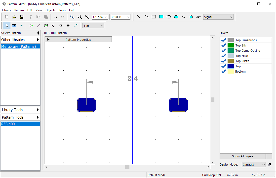
Notice that you can select the side for the surface pads, i.e. place them on the bottom side of the PCB. Select pad(s), right-click on one of them, and select Change Side from the submenu. Select the current side for placing new pads and shapes on the Objects toolbar (drop-down box with the "Top" text) or on the Layers panel.
We need the first pad to have custom pad properties. Right-click on the first pad, and select Properties from the submenu (if the pad is not highlighted while hovering over it, you're not in the default mode – right-click on any free spot or press on the Objects toolbar). In the pop-up Pad <Number> dialog box, select the Type / Dimensions tab, and uncheck Use Pattern's Standard Pad Properties box to enable pad’s custom settings.
Polygon pads
Let's create a hexagonal-shaped pad. The fastest way to achieve that would be selecting an appropriate (Polygon1) template, but let's practice a bit. Do not assign any template, change type to Through-Hole, shape to Polygon, width and height to 0.09 inch and pad hole diameter to 0.04 inch, then press Points to open the Polygon Points dialog box. Here you can create regular or custom polygon shapes that are not available in the templates drop-down list.
Select: Regular, 8 Sides, and specify 0.045-inch Radius. Edit custom shapes with the table below or visually in the preview field (drag and drop the polygon's points).
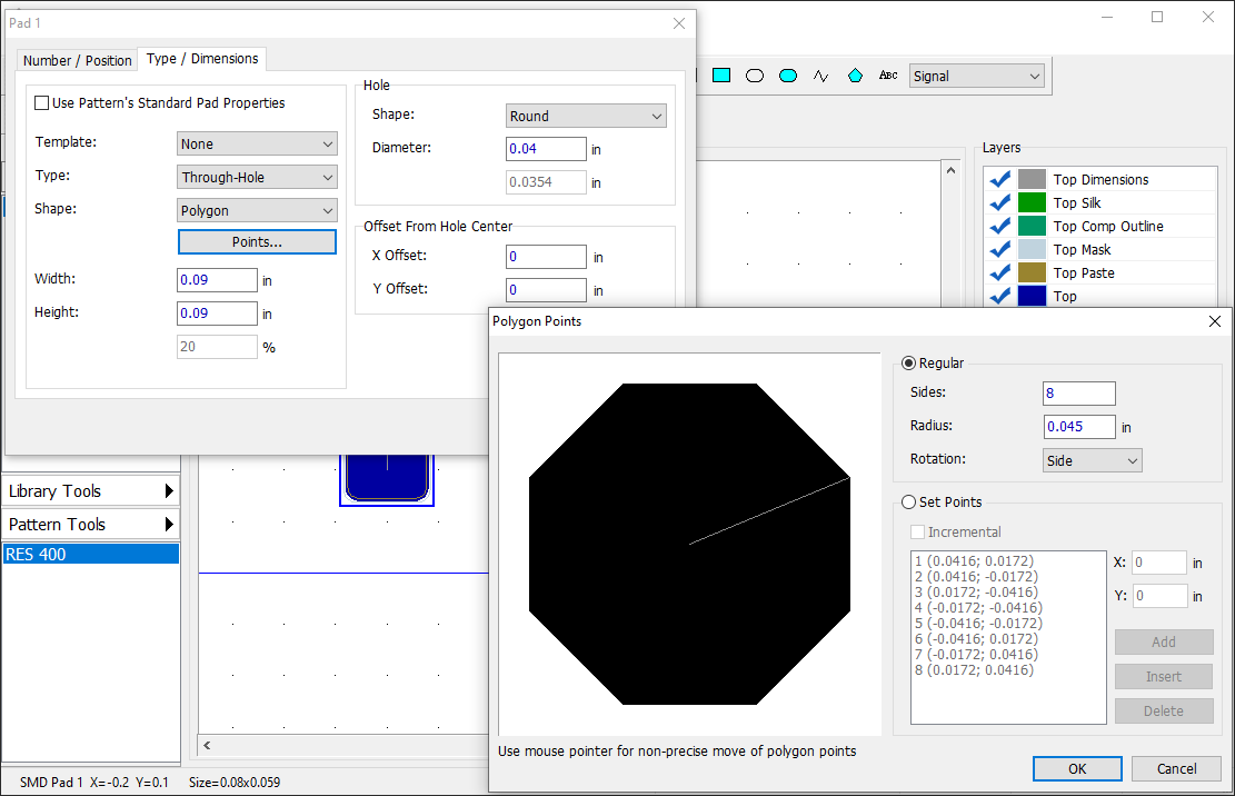
Press OK to apply the polygon shape.
You can change pad coordinates and angle in the Number / Position tab of this dialog box, but do not do that. Press OK. Changes will apply to all selected pads.
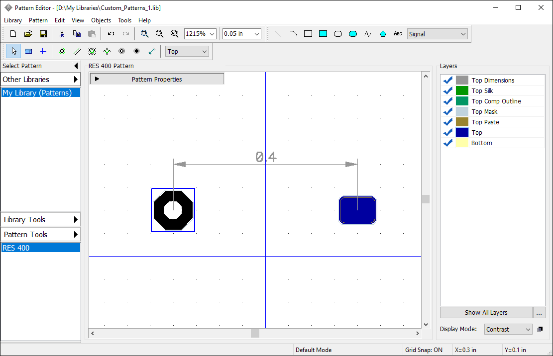
There is also another way to create polygon pads, select the Polygon tool on the Drawing toolbar and draw a shape directly on the design area. Make sure that the shape is on the signal layer (select Signal from the drop-down list on the Drawing toolbar or on the Layers Panel prior to drawing or change shape layer in the shape properties dialog box after placement – right-click on the shape and select Properties from the submenu). When the shape on the signal layer is ready, right-click it, and select Convert to pad from the submenu. This options is visible only for Polygon drawing tool.
Please define the following properties for the pads:
the first pad – 0.09x0.09, Through-Hole, Rectangle, hole – Round, diameter – 0.04;
the second pad – 0.09x0.09, Through-Hole, Obround, hole – Round, diameter – 0.04.
Now let's place a silkscreen for this resistor. Click Rectangle button on the Drawing panel, make sure Top Silk layer is selected. Place a rectangle by clicking in two key points on the design area. Note that DipTrace displays size parameters while placing a shape.
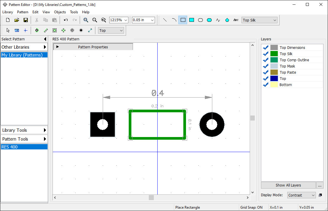
Now disable the rectangle placement mode (right-click on the free spot or press button).
Silk shape looks a bit small for this pattern. There are several ways to change it: 1) right-click on the shape, select Properties, and enter new Width and Height values in the pop-up dialog box; 2) drag-and-drop shape's key points (to use this option disable Snap to Grid option in the View menu to be able to place shape between the grid points or change the grid size). We will use the last method. Let's change the grid size to 0.025 inch with Ctrl+Minus Sign hotkeys or with the grid box on the Instruments toolbar, then hover over rectangle's key points, and resize the shape (the mouse cursor shows possible directions).
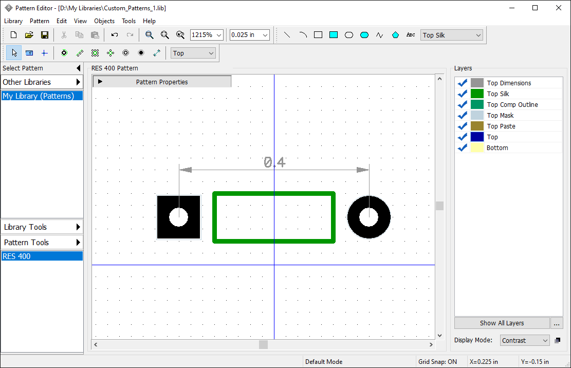
Center the pattern by selecting "Edit / Center Pattern" from the main menu or Ctrl+Alt+C.
To show pad numbers, select "View/ Pad Numbers/ Show".
The resistor is ready.
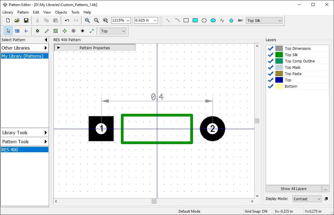
Try to rotate and mirror the first pattern of your library, select "Edit / Rotate Pattern" to rotate and "Edit / Flip Pattern / Vertical or Horizontal" to mirror it.
Press Save on the Standard toolbar. We will attach 3D model for this resistor in the next topic of this tutorial.
36. Attaching a 3D model
There are three options for attaching a 3D model in DipTrace: you can use a STEP file with a 3D model of your component; apply a model from Pattern Generator (works for patterns created with this tool); or create a model by component outline (this option works best for surface-mount devices since a 3D shape with defined parameters is created to mimic an SMD).
We are going to use the first option now.
Please make sure that you have downloaded and installed free 3D Models package from the DipTrace official website, which contains more than 10 000 3D models for various components.
When a component footprint (pattern) is ready, we can attach a 3D Model. Press  button on the Pattern Properties panel. In the pop-up dialog box press All Models button and the list of all available 3D models will pop up, 3D models are sorted by libraries. We will probably find an appropriate resistor model in the _General library. Scroll it down to find the res-10.16_5.1x2.5.step model, left-click it, and it will appear over the footprint. Sometimes you might need to map a 3D model respective to the footprint (see below).
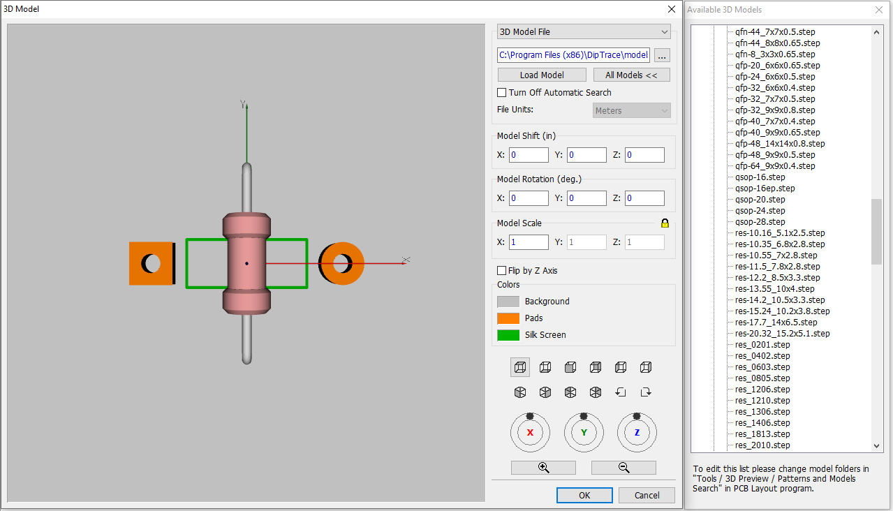
Mapping a 3D model
DipTrace automatically places a 3D model to fit the pattern's drawing, however, sometimes you may need to adjust 3D model location or the scale. Just enter appropriate values into the corresponding fields on the 3D Model Properties section (shift, rotation angle, and scale for each axis). In our case, we see that we need to rotate the resistor 90 degrees and shift it up a bit. Specify 90-degree Z Angle and 0.03 inch Z Shift. You can rotate a 3D model by three axes, zoom in / out, and pan 3D Model preview with the mouse (left, right and wheel clicks). You can also use side and isometric view buttons for quick change of 3D display perspective or rotate the model by three axis with the wheels at the bottom of the window.
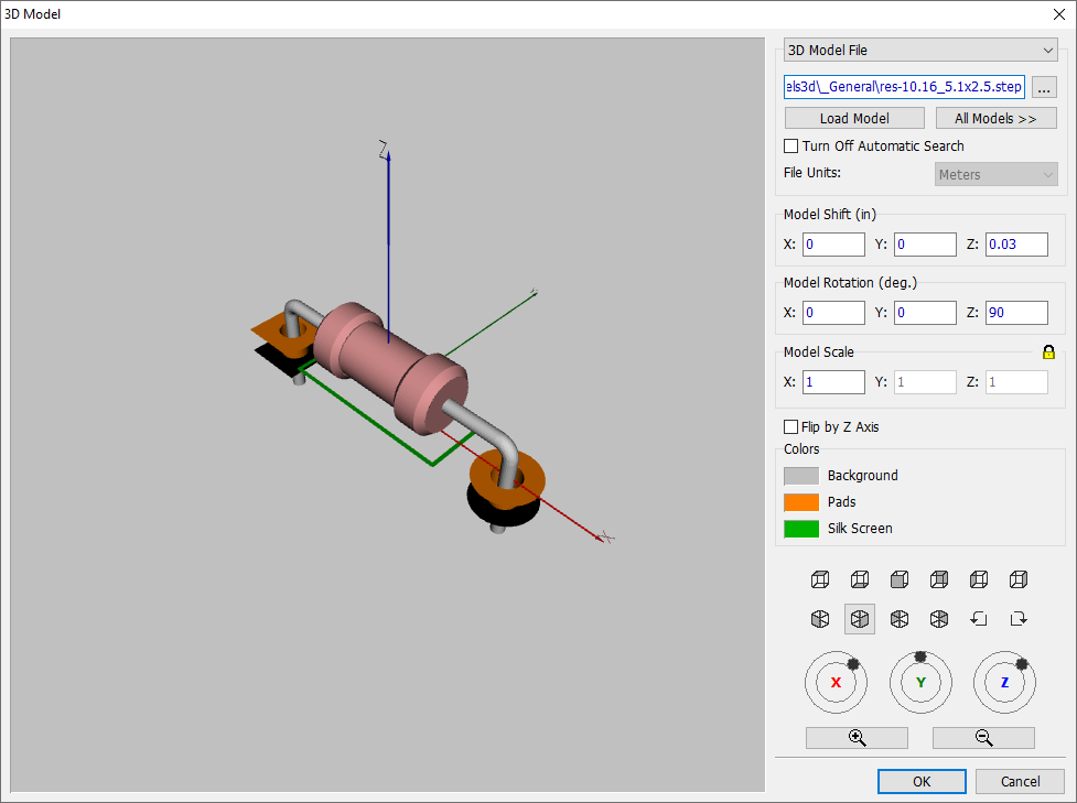
Press OK to attach a 3D model, and then save the pattern library. More details about DipTrace 3D Module later in this tutorial and in the DipTrace Help ("Help / Pattern Editor Help" from the main menu).
37. Automatically (Pattern Generator)
|
There's one more way to create a pattern. And now we'll explore how to make a footprint automatically. But before we start, let's add a new Pattern project to our library. Make sure My Library (Patterns) in User Patterns ( or Other Libraries) group is selected. Go to Pattern menu and select Add New to "My Library (Patterns)" library. Next, we have to launch Pattern Generator.To do that select IPC-7351 from the Style drop-down on Pattern Properties panel. Once selected, IPC-7315 Pattern Generator button appears right below. Click it to start the Generator. |
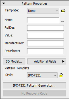
In Pattern Generator we'll make a footprint for HVR37 resistor with copper termination wire, using this datasheet.
First, select Through Hole device type. Next, choose Axial from the Family list on the left side of the dialog.
Now move on to the central part of the Pattern Generator window. Here we'll have to enter all the key parameters. In the SubFamily drop-down select Resistor. Set measuring units in the bottommost part of the window to mm.
Now open the datasheet on page 2 for dimensions. Check Package View images to find the required parameters.
The first cell - Pitch - is colored green, meaning that this value is optional. We are going to leave it empty and let DipTrace calculate the value.
Fill in the remaining Required cells colored red: Amax - 4 mm (this value is not available in the datasheet, so we will assume that A = E = resistor diameter), bmin - 0.67 mm, bmax - 0.73 mm, Dmax - 12 mm, Emax - 4 mm.
Basically, those values are enough to generate a footprint with all other parameters set by default.
For more details on customization of parameters for component generation, please see Pattern Editor Help manual.
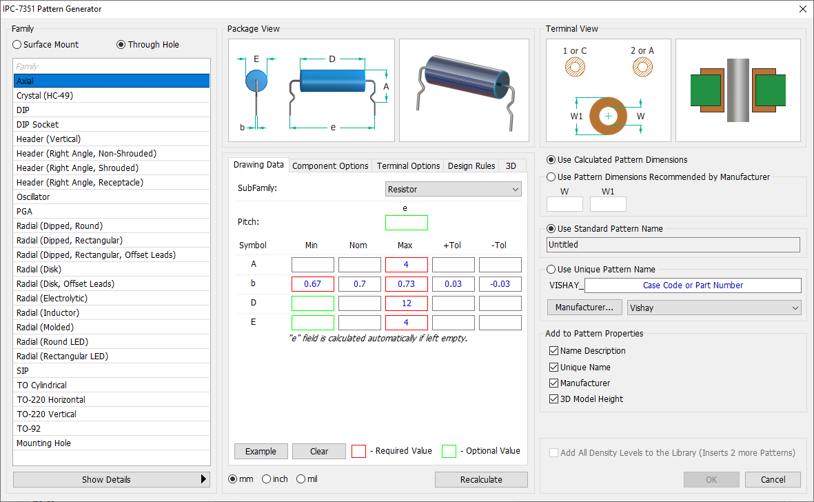
Press Recalculate button and DipTrace will calculate Pattern Dimensions (see the right-hand area of the Generator) based on IPC-7351 Standard, however, you can always change the calculated values for the ones recommended by the manufacturer.
The software has also generated a Standard Pattern Name, you can edit it or opt for using a Unique Pattern Name. Let's choose the latter option. Type-in HVR37 and make sure to choose a Manufacturer from the list, in our case it's Vishay. Note that Use Unique Pattern Name option requires specifying a manufacturer, otherwise the pattern will not be generated.
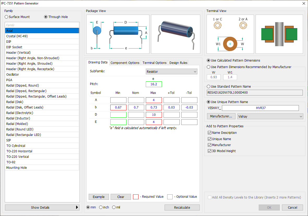
Press Recalculate button again and then OK - and DipTrace will generate the pattern with a 3D model.
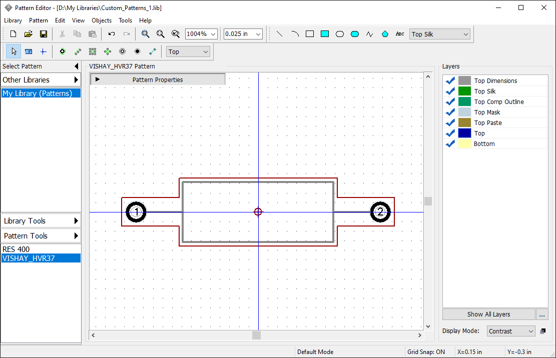
Designing BGA-144/13x13
Designing BGA and SOIC patterns
38. Manually
Press  , then select Add New Pattern to My Library (Patterns) Library on the Library Manager panel. This will add an empty pattern to the library. The pattern is selected. We will create BGA-144/13x13 (x0.8_10x10) pattern using available pattern types and automatic pad numeration. Maximize the Pattern Properties panel and type in the pattern's name.
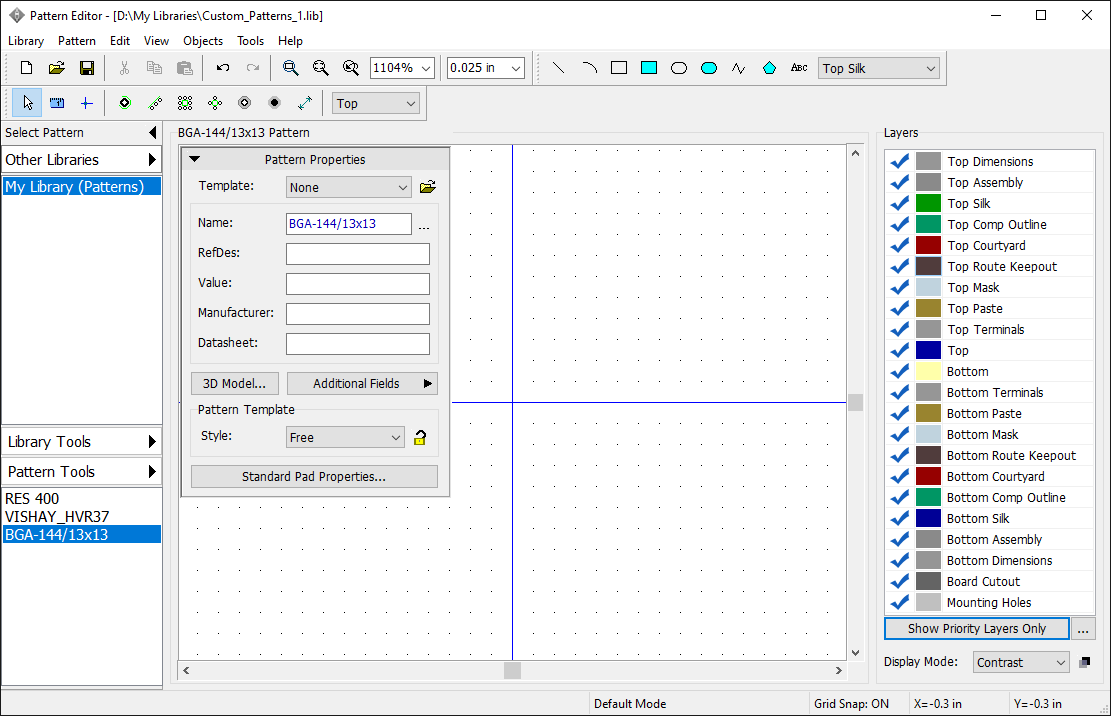
Press , if you want to add Name Description and Unique Name for your pattern.
Change units to mm, press Shift+U hotkeys. Change the Grid size to 0.635 mm.
Go to "Pattern / Standard Pad Properties" from the main menu and set: Type: Surface, Shape: Ellipse, Width: 0.45 mm, Height: 0.45 mm. Press OK to apply changes to default pad properties. On the Pattern Properties panel set: Style: Matrix, Columns: 13, Rows: 13, X Pad Spacing: 0.8 mm, Y Pad Spacing: 0.8 mm. 13x13 pad matrix and pad spacing dimensions appear on the design area.
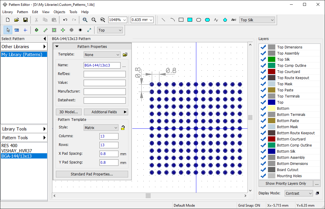
Click  button on the Pattern Properties panel to prevent accidental changes. Minimize the Pattern Properties panel. Pan design area if necessary with the right mouse button or zoom with the mouse wheel. For the BGA-144/13x13 pattern, we should delete 5x5 rectangle of pads in the center, like in the picture below. Select these pads using the box selection (move mouse to the upper-left corner, hold down the left mouse button, move to the bottom-right and release the button), then press Delete key on the keyboard to delete selected pads.
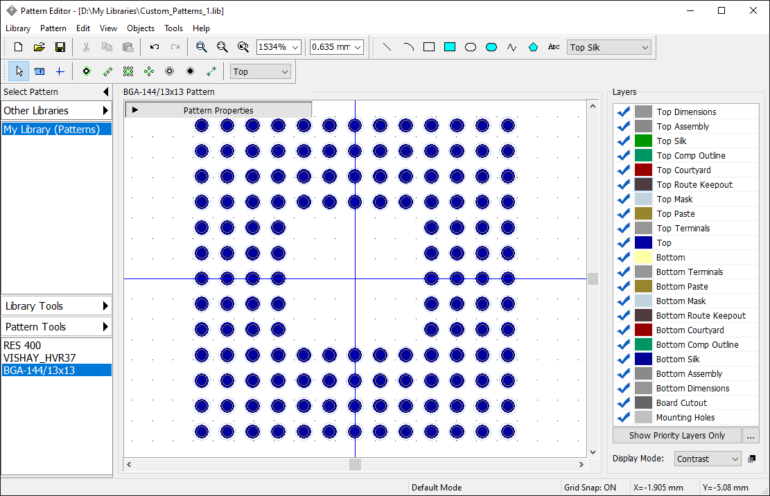
Select "View / Pad Numbers / Show" from the main menu to display pad numbers. Notice that our matrix has 1 – 169 numbers with some missing numbers in the center. This is not right. BGA pads should be A1, A2, A3 etc. Select all pads (Ctrl+A or a box selection), right-click on one of the pads, and choose Pad Array Numbers from the submenu. In the pop-up dialog box, select Type: BGA Matrix, keep other settings, and press OK button.
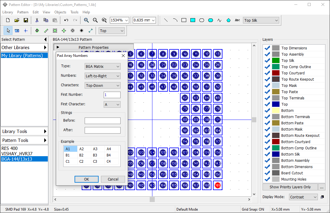
Now pad numeration is correct.
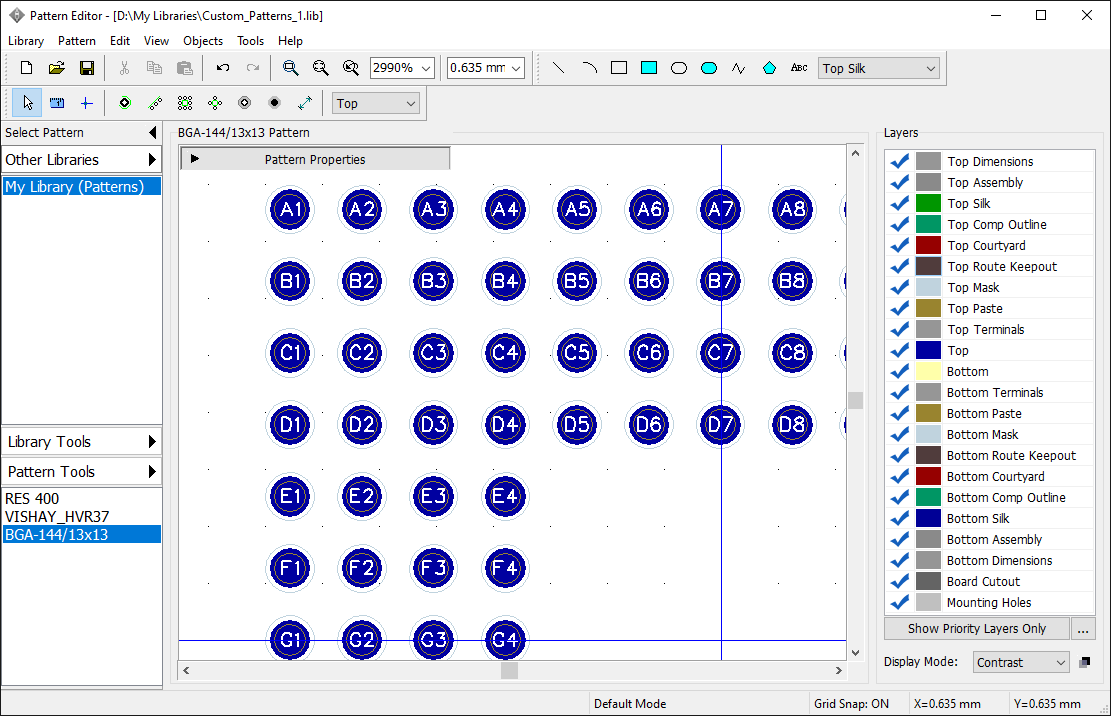
Notice that for Contour type of numeration the first pad will be the one you right-clicked on. This allows the user to numerate contour pads (QUAD patterns) starting from the upper-left, center or any other pad of the pattern.
Now draw a silkscreen for the pattern (like in the picture below), using the tools on the Drawing toolbar. Change grid size with Ctrl+Plus Sign, Ctrl+Minus Sign or turn it OFF/ON with F11 hotkey. You can move objects by dragging and dropping them.
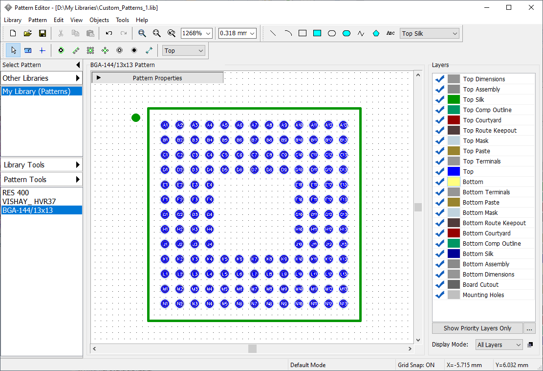
BGA pattern is ready. You can attach a 3D model now.
Attaching 3D Model from file
In the situations, where there is no exact model in the standard 3D model libraries, you can use similar ones because usually we don't need 100% precision for a 3D model. DipTrace allows the user to attach any 3D models in *.3ds, *.wrl, *.step, and *.iges formats to any footprint. You can download models from the component manufacturers' websites or create them in any 3D CAD.
Press button on the Pattern Properties panel.
If you have an appropriate model on your computer click button, select 3D model file on your computer, and press Open. You can also enter 3D model's disk address, and press Load Model button – a 3D model will appear in the preview area. Change 3D Model Properties in case the model does not correspond exactly to the footprint.
For example, we have decided to take the bga-144_12x12x1.27_17x17.step 3D model from the BGA library in the standard 3D model package and scale it down a bit to fit the footprint (see the picture below).
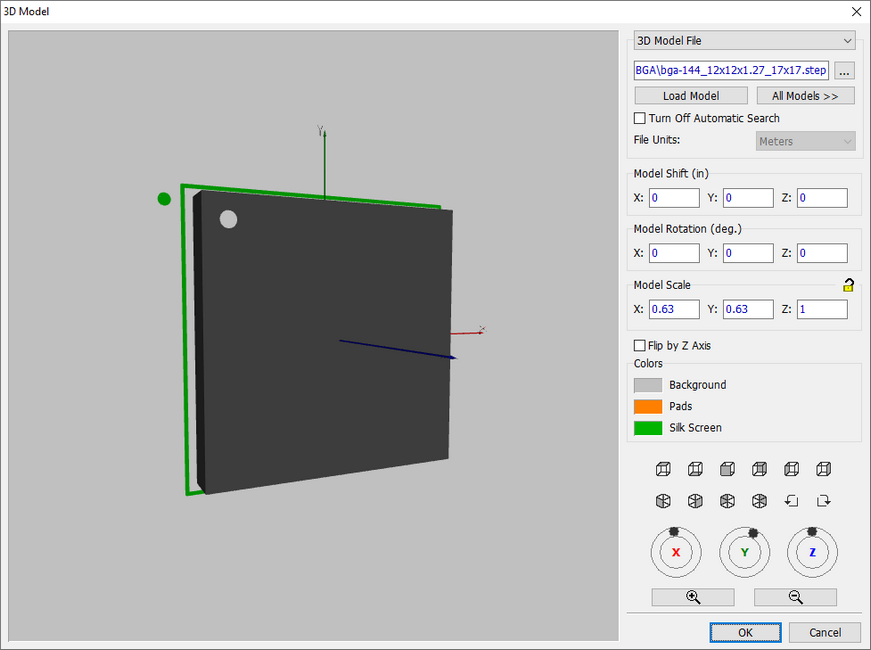
Try to enter different values into various fields and you will understand how to adjust model location. Press OK. Notice that button glows green when the pattern has a 3D model attached.
Save the pattern library (Ctrl+S or Save button on the standard toolbar).
Creating 3D Model by component outline
Another option is to create a 3D model by component outline. This is a particularly handy option, especially for SMD components. To place the outline, go to Objects/ Precize Shape Placement. In the pop-up set the following parameters: Shape Type - Rectangle; Layer - Top Outline; Anchor Point - Center; Height and Width - 11 mm and click Place.
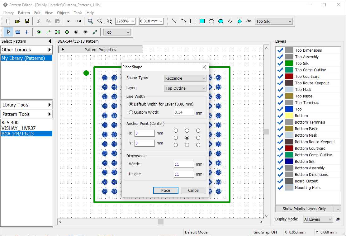
Once the outline is placed, press 3D Model button on Component Properties panel. In the pop-up, select By Component Outline option in the drop-down list at the top of the window, and set Model Height 1 mm. DipTrace will place a 3D shape, following the outline of the footprint. Click OK.
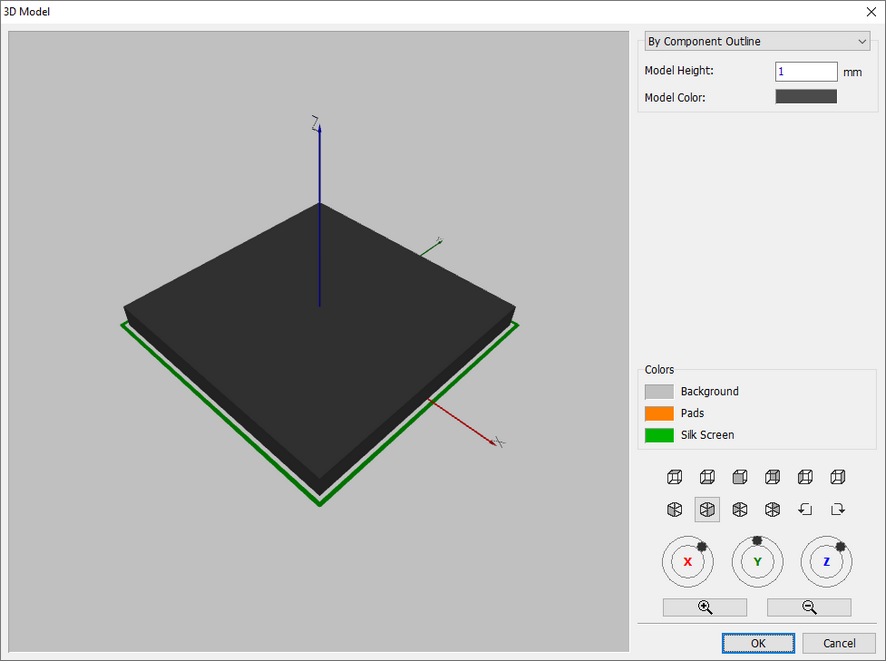
39. Designing BGA Automatically
Now we are going to use Pattern Generator to create a BGA footprint automatically.
Let's create a pattern for a 16-Channel, Current-Input Analog-to-Digital Converter, using this datasheet.
First, we have to add a new Pattern to our library. Make sure My Library (Patterns) in User Patterns group is selected. Go to Pattern menu and select Add New to "My Library (Patterns)" library.
Next, launch Pattern Generator - select IPC-7351 from the Style drop-down on Pattern Properties panel. Once selected, IPC-7315 Pattern Generator button appears right below. Click it to start the Generator.
Select the Family: Surface Mount/ BGA. Press Clear button if the cells in the Drawing Data tab are filled with example values. Here we'll have to enter all the key parameters of the device. Set measuring units in the bottommost part of the window to mm.
Now open the datasheet on page 27 for dimensions.
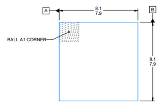
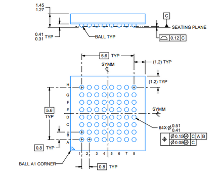
Check Package View images to find the necessary parameters.
Fill in the Required cells colored red:
Pin Count: D - 8, E - 8.
Pitch: 0.8 mm.
Pin Numbering: A1-B1-C1... in Row.
Terminal Type: Collapsing Ball.
Amax - 1.45 mm.
There's no the required bnom value, so let's enter bmin - 0.41 mm and bmax - 0.51 mm and let DipTrace calculate the value.
D/E min - 7.9 mm, D/E max - 8.1 mm.
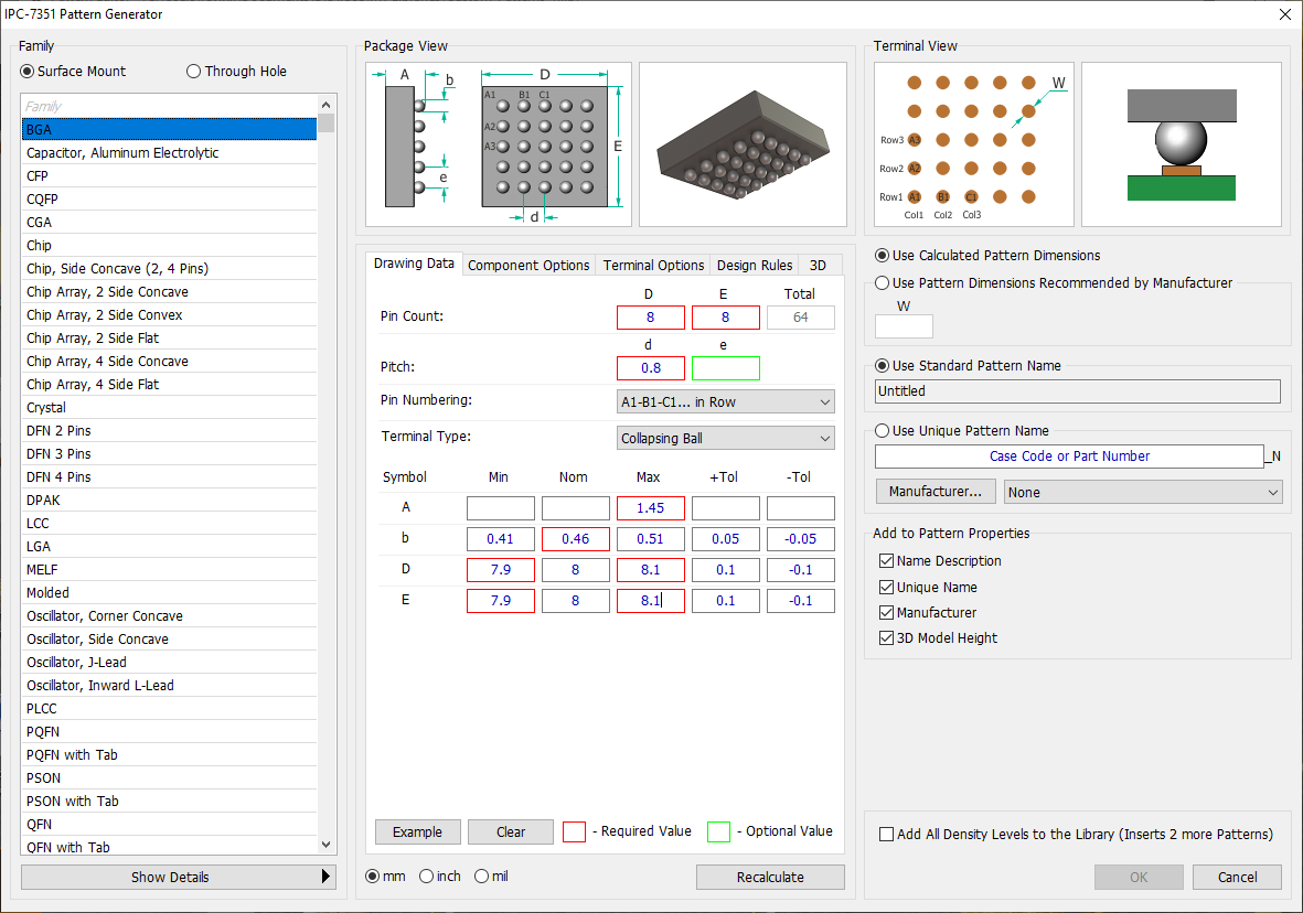
Those values are enough to generate a footprint with all other parameters set by default. Press Recalculate and the OK button.
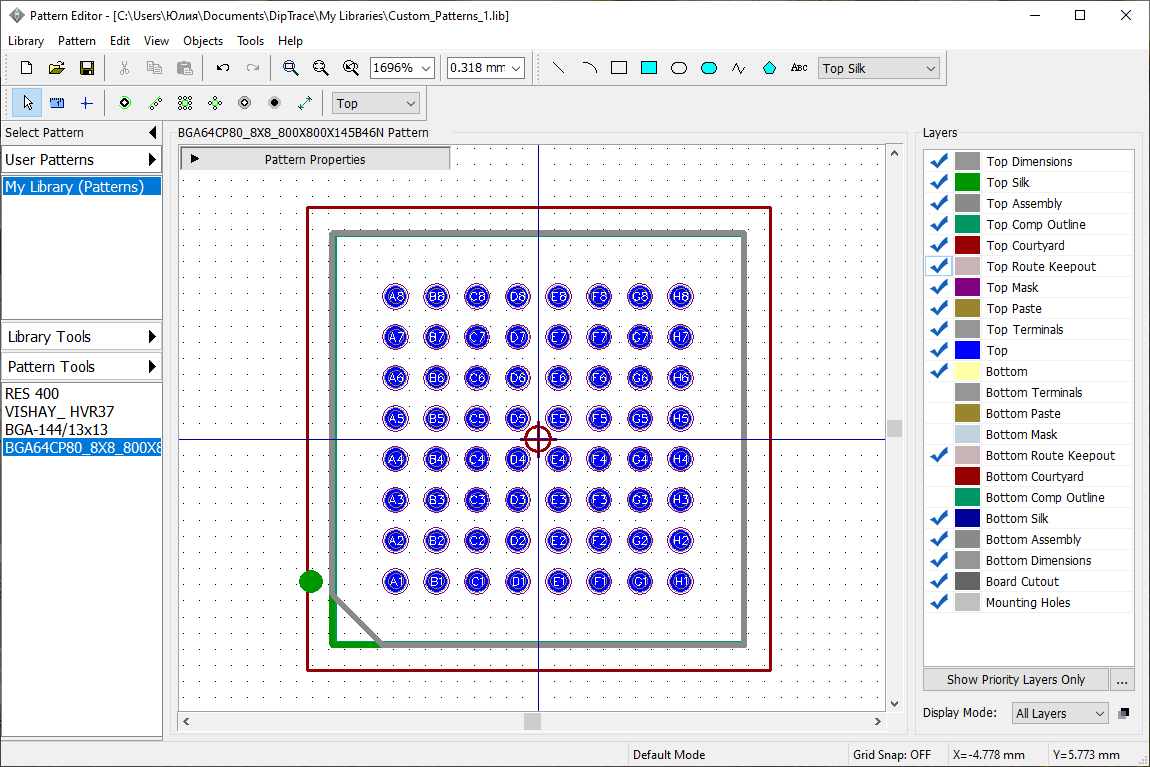
For more details on customization of parameters for component generation, please see Pattern Editor Help manual.
DipTrace has also generated a 3D model of the device. You can check it by clicking 3D Model button on Pattern Properties panel.
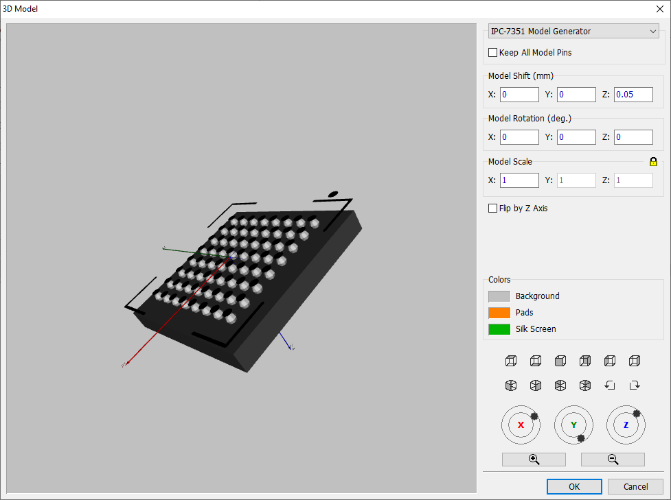
40. Designing SOIC-28 pattern
Now that you are familiar with all the basics, we can practice creating a component manually according to a datasheet. It's gonna be the simple Microchip PIC18F24K20 component with SOIC-28 pattern.
When you start creating a component from a scratch, and you don't have an appropriate pattern, always start from the pattern creation and then proceed to component's symbol.
We start from making a pattern. Add a new pattern to the library ("Pattern / Add New Pattern To "My Library (Patterns)" Library" from the main menu), then enter the name – "SOIC-28" and RefDes – "IC".
Select Style: Lines on the Pattern Properties panel, and set Number of Pads: 28. In our case pads are way too small for this pattern.
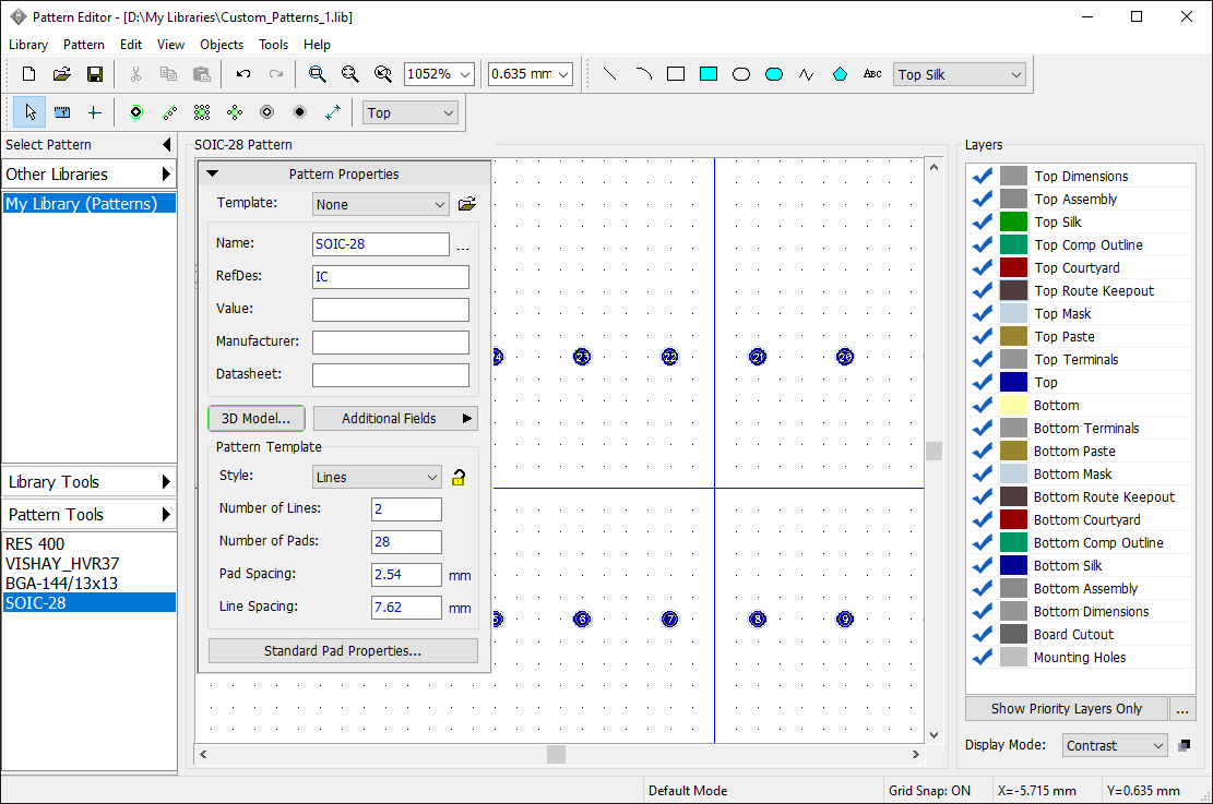
We should define correct pad spacing, line spacing, and pad settings. You can find SOIC-28 (7.50 mm) footprint dimensions on the Microchip package specifications PDF at the Microchip's website (page 197 in the latest revision at the moment of writing this tutorial) or you can take the SOIC-28 pattern from standard DipTrace libraries as an example.
Define default pad settings (press Standard Pad Properties button to open the dialog box): Type: Surface, Shape: Rectangle, Width: 0.6 mm, Height: 2 mm. Press OK. Then specify Pad Spacing: 1.27 mm and Line Spacing: 9.4 mm on the Pattern Properties panel.
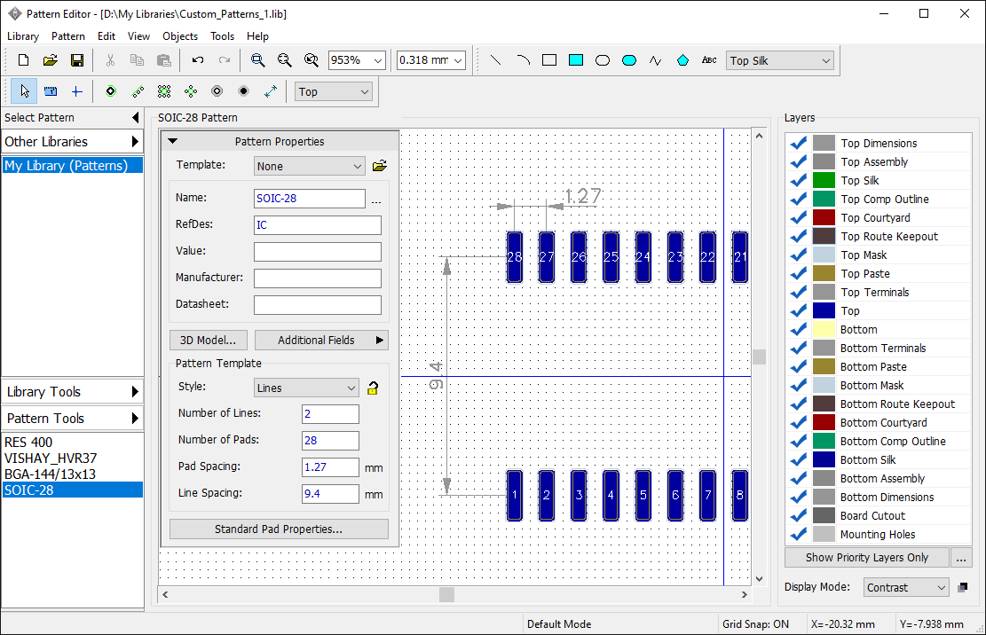
Pad numbers are correct, we don't need to renumber them. Lock pattern properties to avoid accidental changes. Draw a silkscreen (like in the picture below), using line/polyline and arc tools found on the Drawing toolbar (turn ON/OFF the grid, change grid size, and hide Pattern Properties panel if you need).
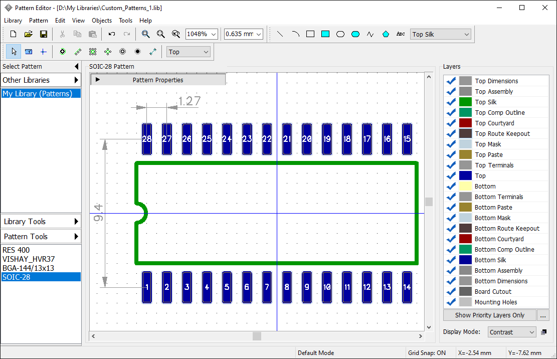
Datasheet requires the pattern to be rotated 90 degrees – select "Edit / Rotate Pattern" from the main menu or Ctrl+Alt+R. Attach soic-28_300mil.step 3D model from the _General 3D Models category.
We will attach this pattern to PIC18F24K20 component, which we will create in the Component Editor later in this tutorial.
Remember that you can easily create the same pattern and 3D model using Pattern Generator.
Save this library and close the Pattern Editor.
Component library and editor basics
41. Designing a component library
Open DipTrace Component Editor, i.e. go to "Start / All Programs / DipTrace / Component Editor" in Windows or use DipTrace Launcher on MacOS.
Component Editor allows the user to create / edit and manage components and libraries in DipTrace. Component Editor allows attaching component's pattern to the symbol, but it doesn't allow pattern editing – use the Pattern Editor.
42. Customizing Component Editor
Customizing Component Editor is almost the same as customizing the Pattern Editor. Select "View / Display Origin" from the main menu to show a zero point and X, Y axes (or press F1) if you can't see the origin point. Component Properties panel in the upper-left side of the design area can be minimized or hidden using the buttons on the panel and in the main menu.
On the Component Properties panel, you can define the symbol style (4 styles available): Free (without any specific properties), 2 sides, IC-2 sides, IC-4 sides. The only difference between "2 sides" and "IC-2 sides" is a rectangle shape (IC Symbol) for the last one.
The fields that might look unfamiliar are the Part Type field and the Part field. The part type can be Normal, Power and GND or Net Port. A component can contain only one Power and GND part (if you prefer to hide all power nets of your schematic, then all power pins should be in this part). Net Port is a single-part component, we use net ports to connect wires logically. Net ports are usually applied to Ground or Power nets and schematics with flexible structure (we will design such component later).
The Part field indicates the current part of a multi-part component.
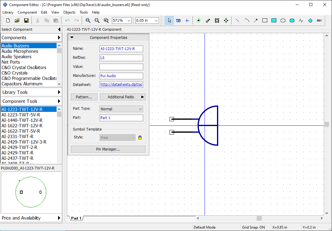
If you need to define pin settings before creating a component, select "Objects / Pin Placement Setup" from the main menu. We will not change these parameters now, but notice that length and X, Y spacing should be divisible by the grid step to create all key points on the grid. We recommend using 0.1-inch grid.
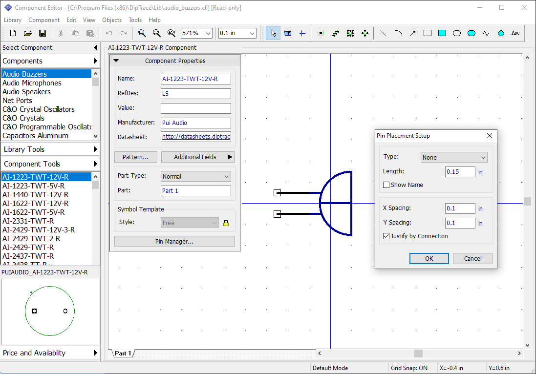
Designing basic components
43. Designing a resistor (component)
Like in the Pattern Editor, first, we need to create a new library because DipTrace won't let you add new components to the standard libraries.
Create library
Press  , then select New Library, in the pop-up dialog box enter the library name, hint, and select the library group. We recommend saving this library in the User Components library group, offered by default. Press OK.
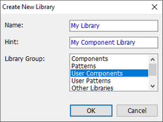
We will design a resistor using the Free style and visual pin placement. Define component name, RefDes, and value "47kΩ", use the corresponding fields on the Component Properties panel. Save the Library on your computer: press the Save button on the Standard toolbar, select location (except the folder with standard libraries), enter a file name, and press Save. The library can be saved in XML format for version control purposes.
After specifying these attributes, please minimize the panel, using the arrow in its upper-left corner.
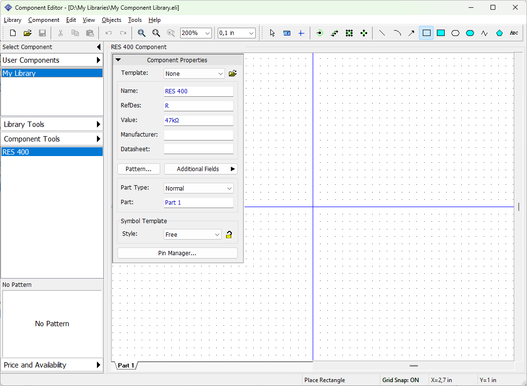
Place pins
Select the Place Pin tool on the Objects toolbar ( button), then move the mouse cursor to the design area, and place two pins with left clicks. Rotate one pin 180 degrees, (select it, and press R twice), make sure that pins are placed by the 0.1-inch grid. Now change the grid to 0.05 inch, select the Rectangle tool, and place graphics for the resistor. DipTrace will show the dimensions of the shape while you are placing it.
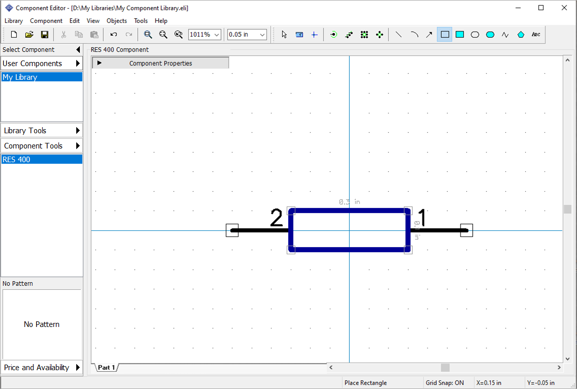
Notice that you can move pin(s) using the drag-and-drop method. If you want to move or rotate several pins, select them first.
You can use the Align Objects tool for automatically placing several objects in a row or column. Select objects on the design area, then select Align Objects from the submenu to set up alignment direction and spacing.
Attach pattern
The symbol of the resistor is ready, but the component is not ready yet. We should attach a pattern to this symbol, otherwise, we will not be able to generate the circuit board from the schematic with this resistor. Select "Component / Attached Pattern" from the main menu or press Pattern on the Component Properties panel. We need to connect this symbol drawing with a pattern drawing created before in the Pattern Editor. Select User Patterns (see "Designing Resistor (pattern)" topic of this tutorial). There should be only one library in that group (My Library (Patterns)). Select it, and select RES 400 pattern that we've created earlier.
Notice that DipTrace automatically creates pin-to-pad connections by numbers. You can review and reassign them if necessary. Connections should be like in the picture below.
To create or redefine pin-to-pad connections, hover over the pin, left-click it, then move the mouse to the corresponding pad, and left-click it to connect them. To delete a connection, right-click on the pin or pad, and select Disconnect pin from pad item from the submenu. When you move the cursor over one of connected pins/pads, both are highlighted. If a component is more complex, use the Pin to Pad table (select pin and type in the corresponding pad number into the Number field below).
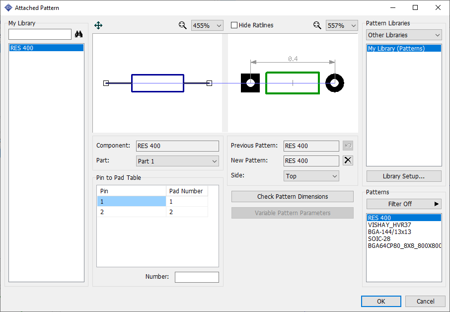
Pin numbers (therefore component's pin to pad connections) can be changed with the Pin Manager (select "Component /Pin Manager" from the main menu) or in the Pin Properties dialog box.
Pattern pad numbers can be displayed by enabling the "Show Pad Numbers" option in the Check Pattern Dimensions. This section also provides a ruler for measuring distances within the pattern, and pad properties are shown when hovering the cursor over them.
If the current pattern is wrong, you can undo to the previous one or delete it by pressing the corresponding buttons (Previous Pattern, New Pattern). Change pattern side with the corresponding drop-down list.
All components of the library are in the left part of the dialog box, this allows the user to attach patterns to several components at a time. However, we don't need this now. Our Library has only one component.
Everything looks good. Press OK to close the Attached Pattern dialog box. The resistor is ready and contains both schematic part and PCB pattern with 3D Model.
Save the component library.
Notice that this is the file with *.eli or *.elixml extension, this means that this is component library file.
44. Designing a capacitor
Select "Component / Add New to "My Library" from the main menu to add a new component to the library.
We will design a capacitor using the 2 sides component style (Style box on the Component Properties panel); type in the component's name "CAP", RefDes – "C", Value – "2µF" . Change component width and pin spacing to 0.1 inch, left and right pins to "1".
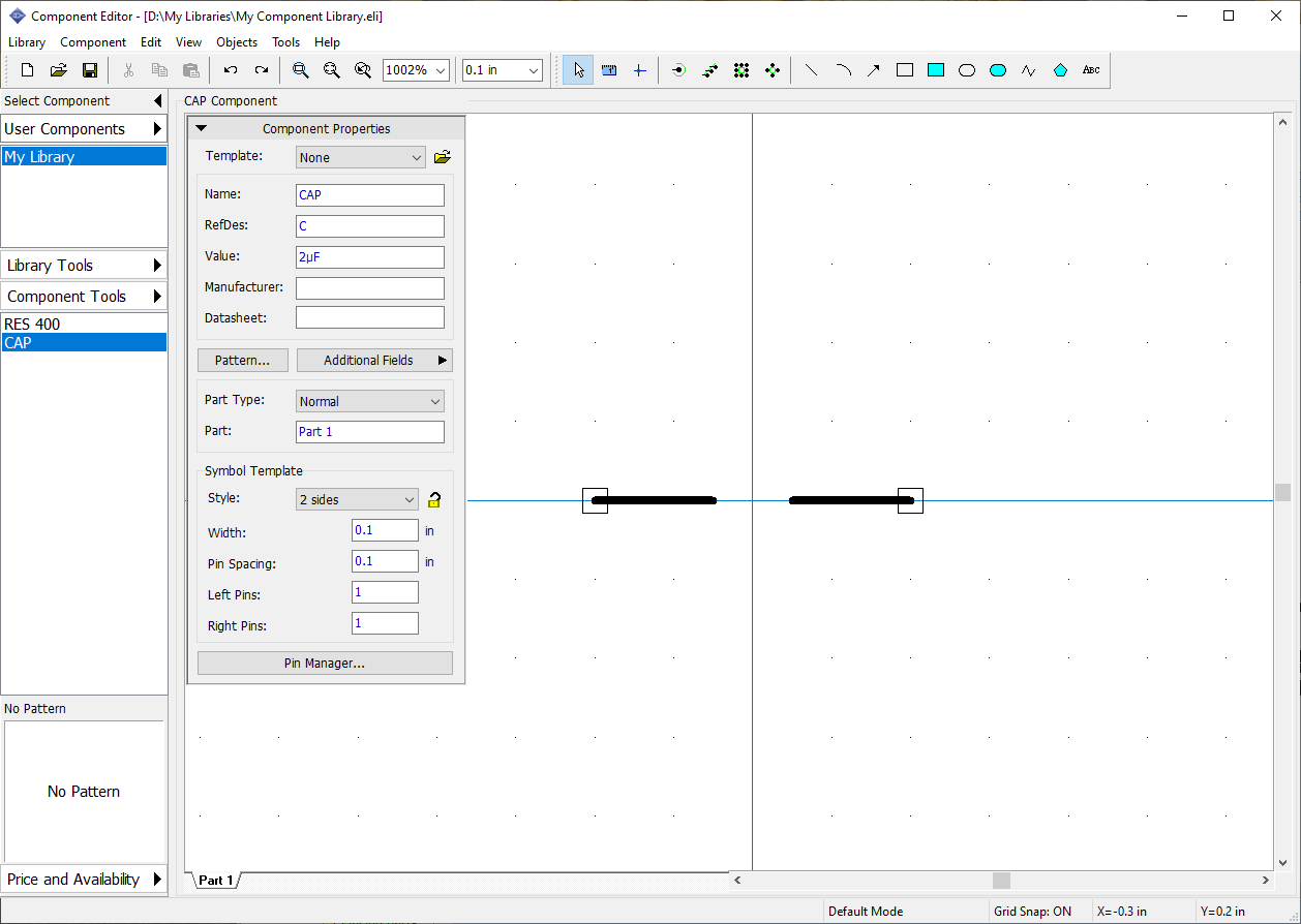
Now please minimize the Component Properties panel, change the grid size to 0.0125 inch, and draw the capacitor's graphics, using three lines and one arc (it's convenient to use Start-End-Radius mode, Counter-Clockwise for placing an arc in this case).
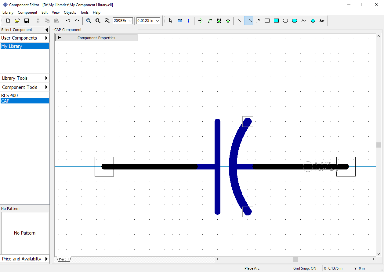
Show pin names for the component symbol, select pins (or select all using Ctrl+A hotkeys), right-click on one of them, and choose Pin Properties from the submenu. In the Pin Properties dialog box, check the Show Name box, and press OK.
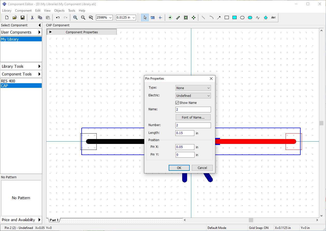
Now you can see the pin names but they are in wrong places (probably overlaying each other) and you need to move them. Select "View / Move Text Tool" from the main menu or press F10, then hover over the pin names, and drag them to new locations one-by-one, then right-click to return to the Default mode.
Notice that you can use such method to move pin names, numbers and part attributes in Schematic.
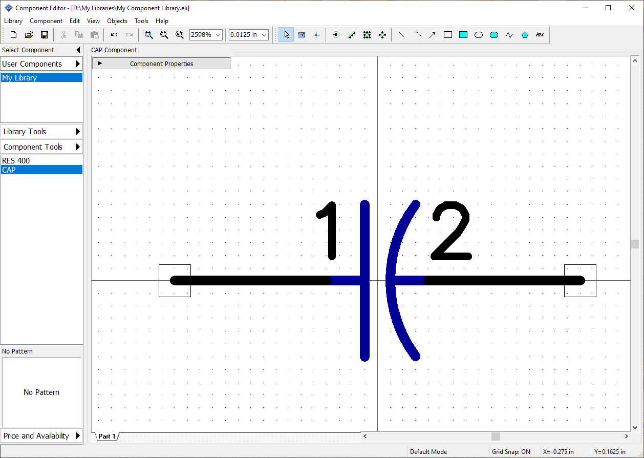
You can show inversion line in the pin name, just hover over the pin with your mouse, right-click, and select Pin Name from the submenu, type in "normal ~invert" text, and press OK, then move the pin name using the move tool (F10 hotkey). The Tilde Symbol (~) in the pin name starts and ends the inversion, so using it you can define the inversion for separate parts (signals) in the pin names.
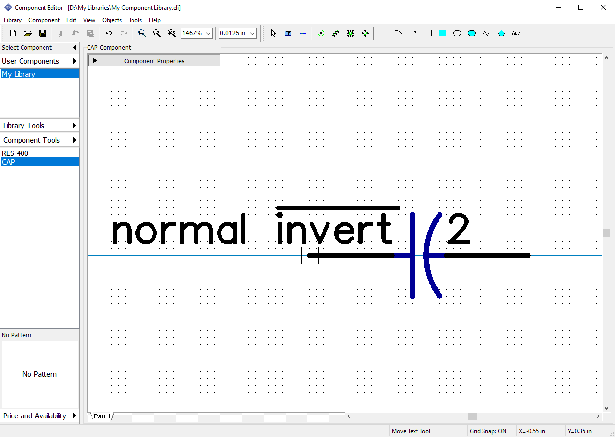
You probably don’t need to see the pin names for simple passive components like capacitors.
Select "Component / Pin Manager" from the main menu to open the Pin Manager dialog box and change "normal ~invert" pin name back to "1". Now hide pin names for both pins: select pin row in the table, and uncheck Show Name box at the bottom of the dialog box. Close the Pin Manager.
Notice that you can change pin numbers (i.e. related pads), coordinates, length, type, and electric type of pins in the Pin Manager dialog box.
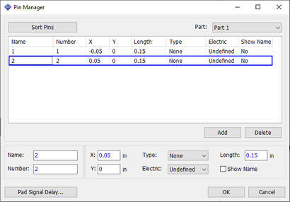
In the Component Editor you can set individual show/hide pin numbers settings for current component ("Component / Pin Numbers" from the main menu) and common program settings (the same as in the Schematic) in "View / Pin Numbers / Show" from the main menu.
Let's show capacitor's pin numbers. If you need to move pin numbers, use the move tool (F10).
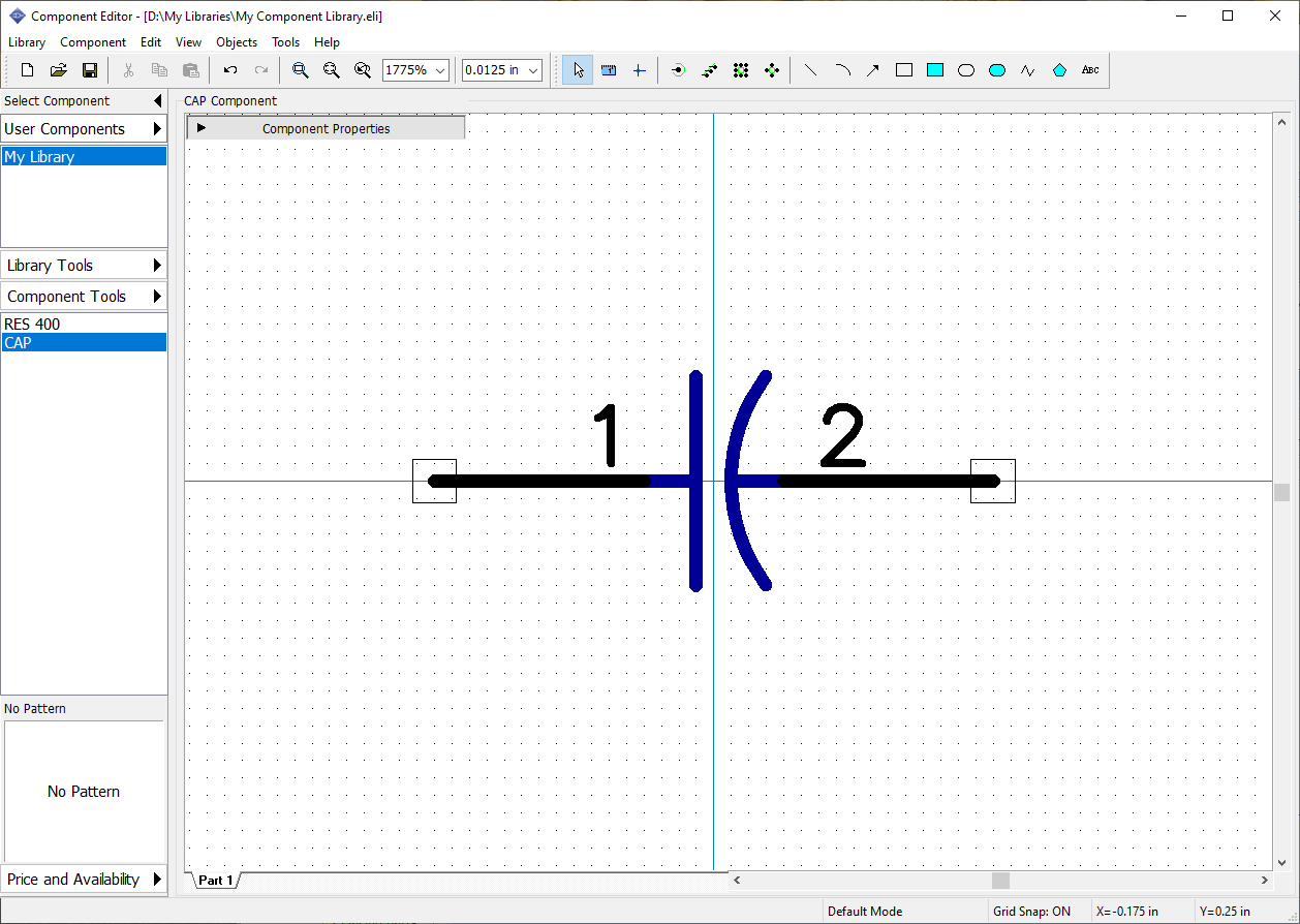
The next step is attaching a pattern to the capacitor. Open Component Properties panel and press Pattern button. We did not create a pattern drawing for this component because we will take an appropriate pattern from the standard DipTrace libraries. Select the Patterns library group, then select Cap Electrolytic Radial library below, and CAPPRD500W60D1050H1450 from the list of patterns. You can use the search filters.
Pin-to-pad connections assigned automatically are good.
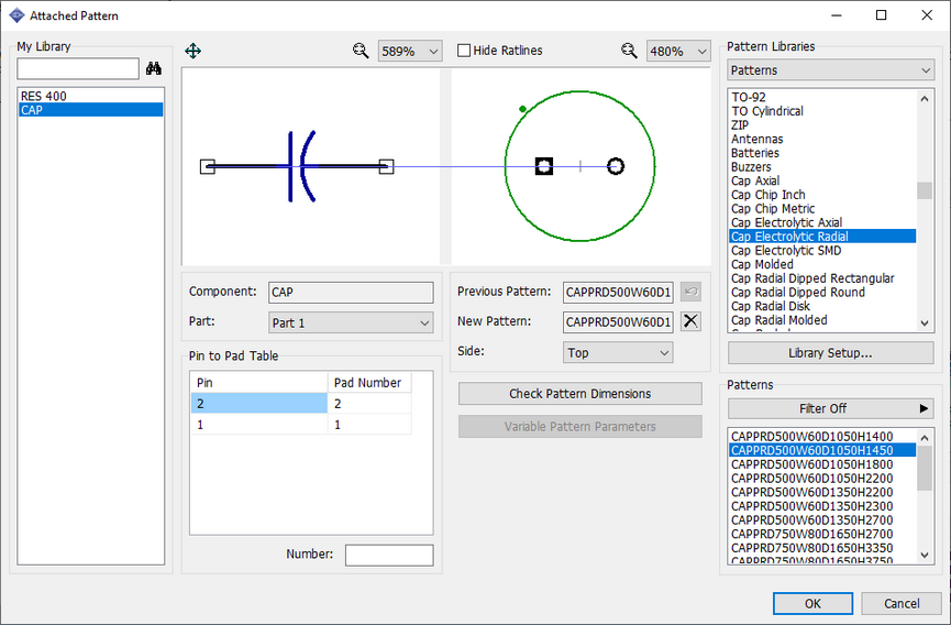
Press OK. The capacitor is ready. Save the changes.
45. Designing VCC and GND symbols
In this part, we will practice in creating net ports by designing VCC and GND symbols.
VCC
Press  , then select Add New Component to "My Library", type in "VCC" in the Name field on the Component Properties panel, and select Net Port in the Part Type drop-down list.
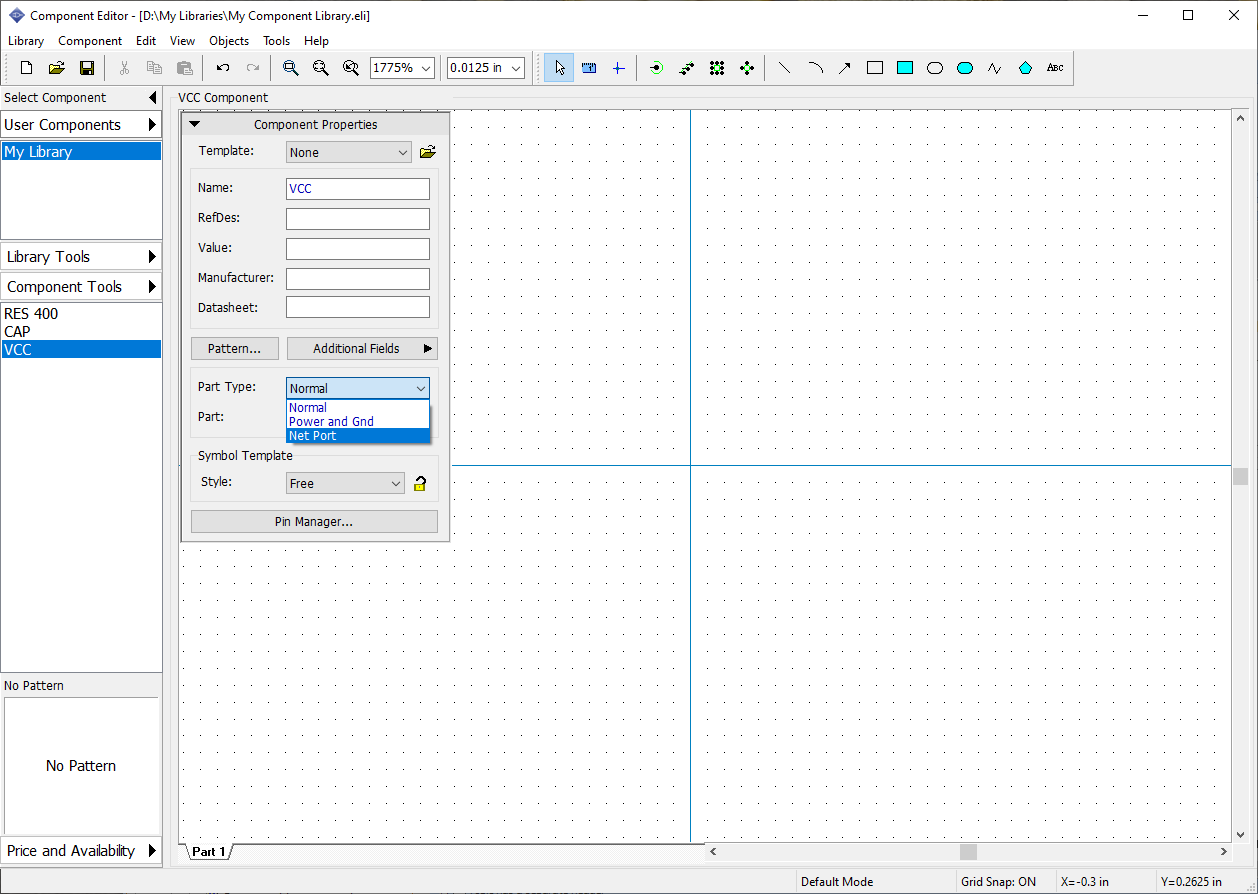
Minimize the Component Properties panel, then press the Place Pin button on the Objects toolbar and place a single pin, rotate it vertically (select it, and press R hotkey). Select the line tool on the Drawing toolbar and draw a line like in the picture below.
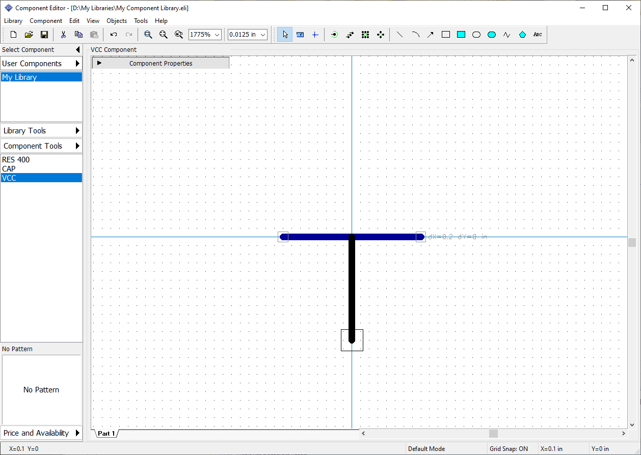
Hide the pin number if it is visible, select "Component / Pin Numbers / Hide" from the main menu. Pin number for the single-pin component looks kind of weird. VCC symbol is ready.
GND
Now add one more component (Ctrl+Ins hotkeys), and create a GND symbol the same way like the VCC symbol.
Select "Edit / Center Symbol" or press Ctrl+Alt+C for GND because in our case its origin is not in the center, so you have to center it to make component's origin hidden by default in the Schematic. Use 0.0125-inch grid to draw a GND symbol's graphics.
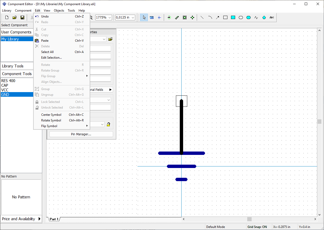
Notice that net ports do not need patterns. This special type of components is used only in Schematic to connect wires without visual connections, net ports do not exist on the circuit board.
Save the library file.
46. Designing a multi-part component
Despite being represented as a single physical package on the circuit board, some electronic components has multi-part schematic symbols. Building a multi-part schematic symbol involves a bit different technique.
Creating a symbol
We will design a simple multi-part component with four "And-Not" symbols, a power part, and attach DIP-14 pattern, which is available in the standard libraries.
Add a new component to the library, i.e. select "Component / Add New To "My Library" Library" from the main menu. Enter the name and Reference Designator.
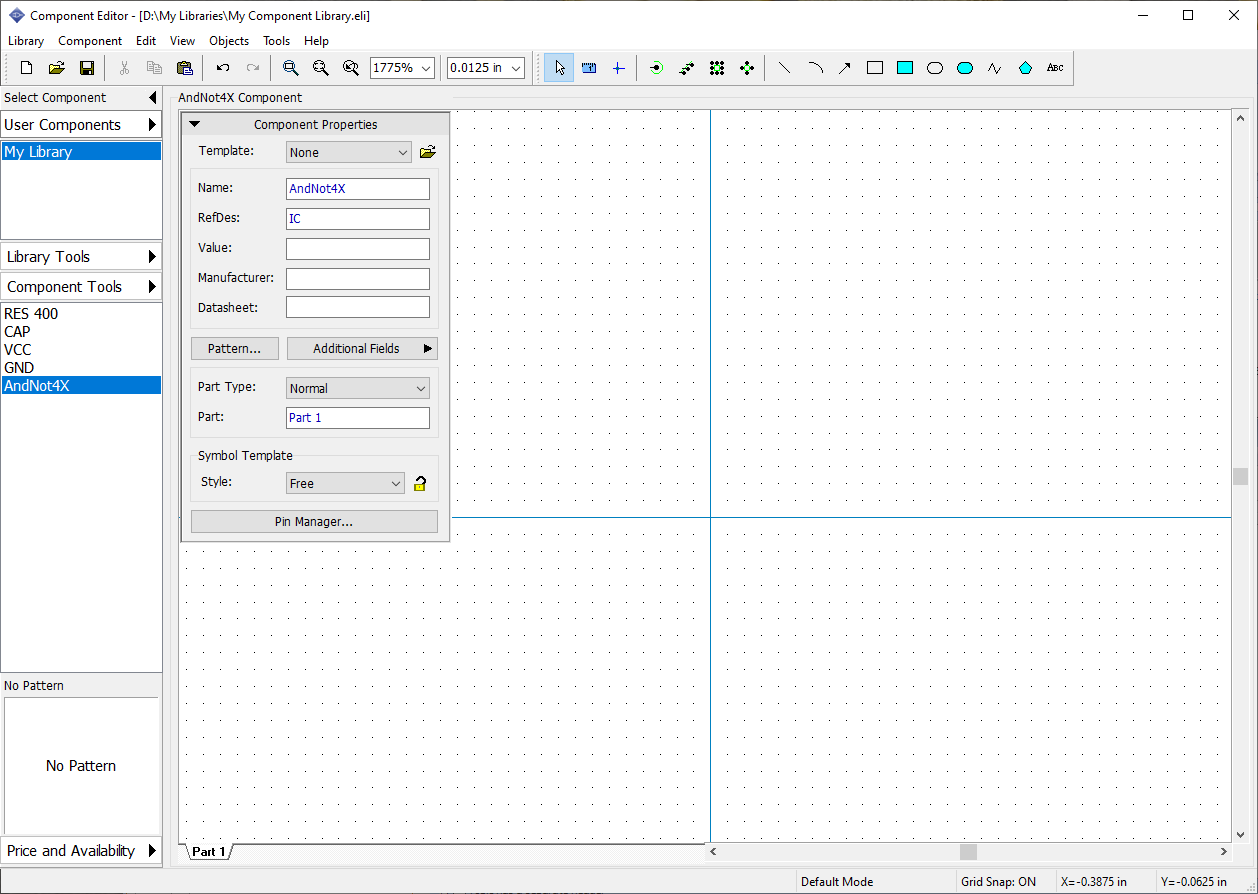
Creating parts
DipTrace allows for creating multi-part components using separate or similar parts. The only difference between these is that similar parts share the same layout of pins and symbol drawing, except the pin numbers (i.e. related pads). We will proceed with similar parts, which, by the way, can be grouped later in the Schematic.
Each part of the multi-part component can be Normal, Power and Ground, or Net Port. Power parts and power nets can be hidden in the schematic capture. Only one power part per component is used.
We will design a component with 4 similar AndNot gates (parts) and one power part that has a different layout (created separately from the similar parts). Select "Component / Create Similar Parts" from the main menu, type "4" in the pop-up dialog box, and press OK to apply. Tabs with the part names have appeared in the bottom-left of the design area (like sheets in the Schematic).
Similar parts are created based on the currently selected part. They share the same name and layout of pins.
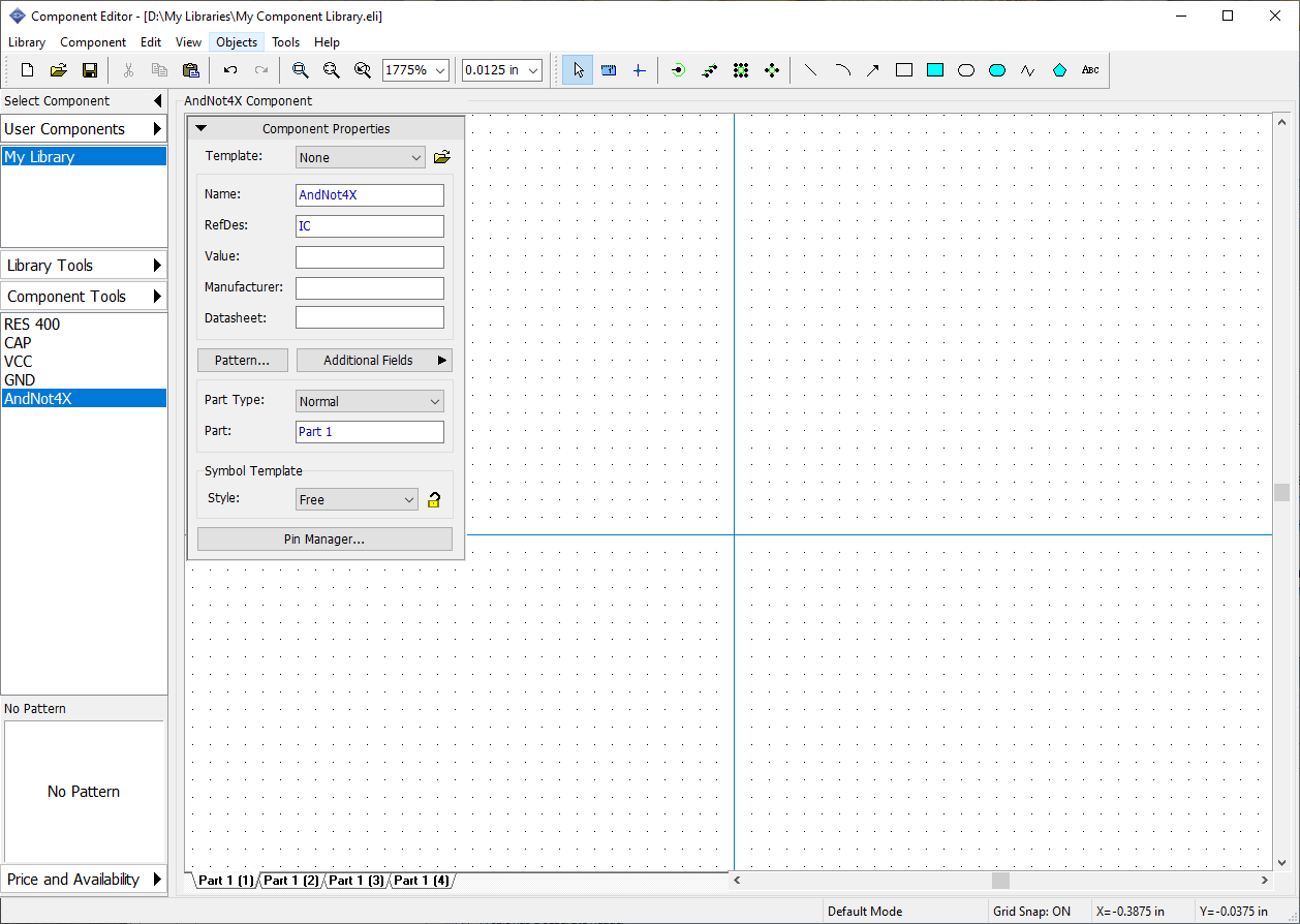
Now you can see the following 4 parts: Part 1 (1), Part 1 (2), Part 1 (3), and Part 1 (4). All similar parts have the same part name. Change it to "AN" in the Part field on the Component Properties panel.
The power part for the component is missing. Power part has a symbol different from the logic gates, this is why we will create it as a separate part (not in the "AN" group of similar parts). Select "Component / Add New Part" from the main menu to add a single part to the component, select new part tab (Part 1) in the bottom-left of the design area, and rename it to "PWR".
Notice that new part is a separate part and does not belong to "AN" group.
Start designing a component with the power part. On the Component Properties panel specify Style: IC - 2 sides, Width: 0.3 inch, Height: 0.25 in, Left Pins: 2, Right Pins: 0, then select Power and Gnd from the Part Type drop-down list. Make general component pin numbers visible ("View / Pin Numbers / Show" from the main menu), if they are hidden.
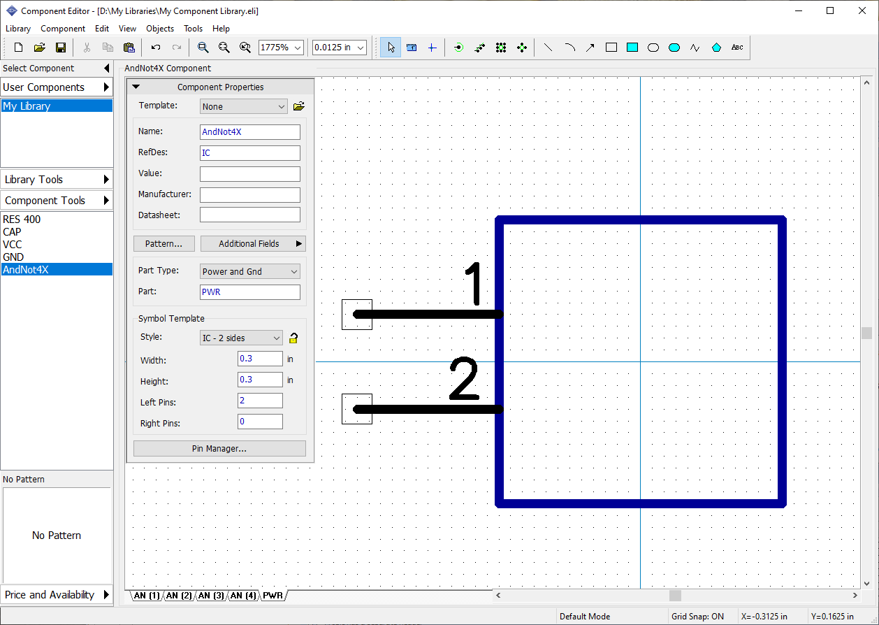
Press the Pin Manager button on the Component Properties panel, and change pin names to "VCC" and "GND", pin numbers to "14" and "7", electric type to Power, the Show Name box should be checked for both pins. Notice that you can change Type, Show Name and Length parameters for multiple pins at the same time.
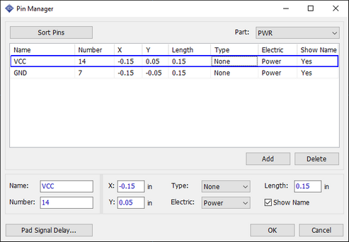
Pin Manager dialog box itself and the width of the rows are resizable. These settings are saved when you close the program.
Now press OK to close the Pin Manager dialog box. Then minimize the Component Properties panel and see the first ready part of the component.
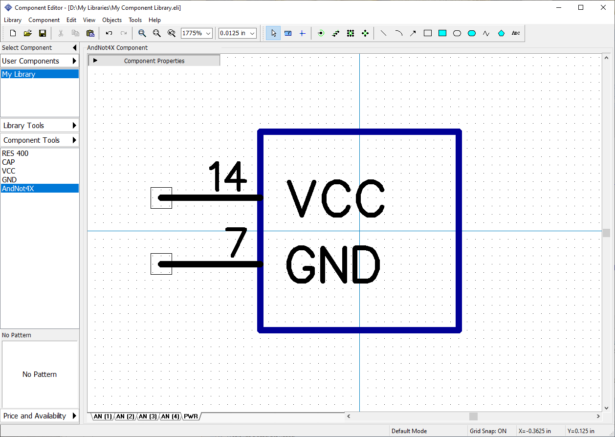
Design the other parts of the multi-part component: select one of the AN parts, maximize the Component Properties panel, and define the following parameters: Style: IC-2 sides, Width: 0.2 in, Height: 0.25 in, Left Pins: 2, Right pins: 1. Now minimize the Component Properties panel again.
Select the text tool on the drawing toolbar (  button), hover over the symbol, left-click, and type "&" character, then right-click to place the text and return to the default mode (see the picture below). Move the text if you need.
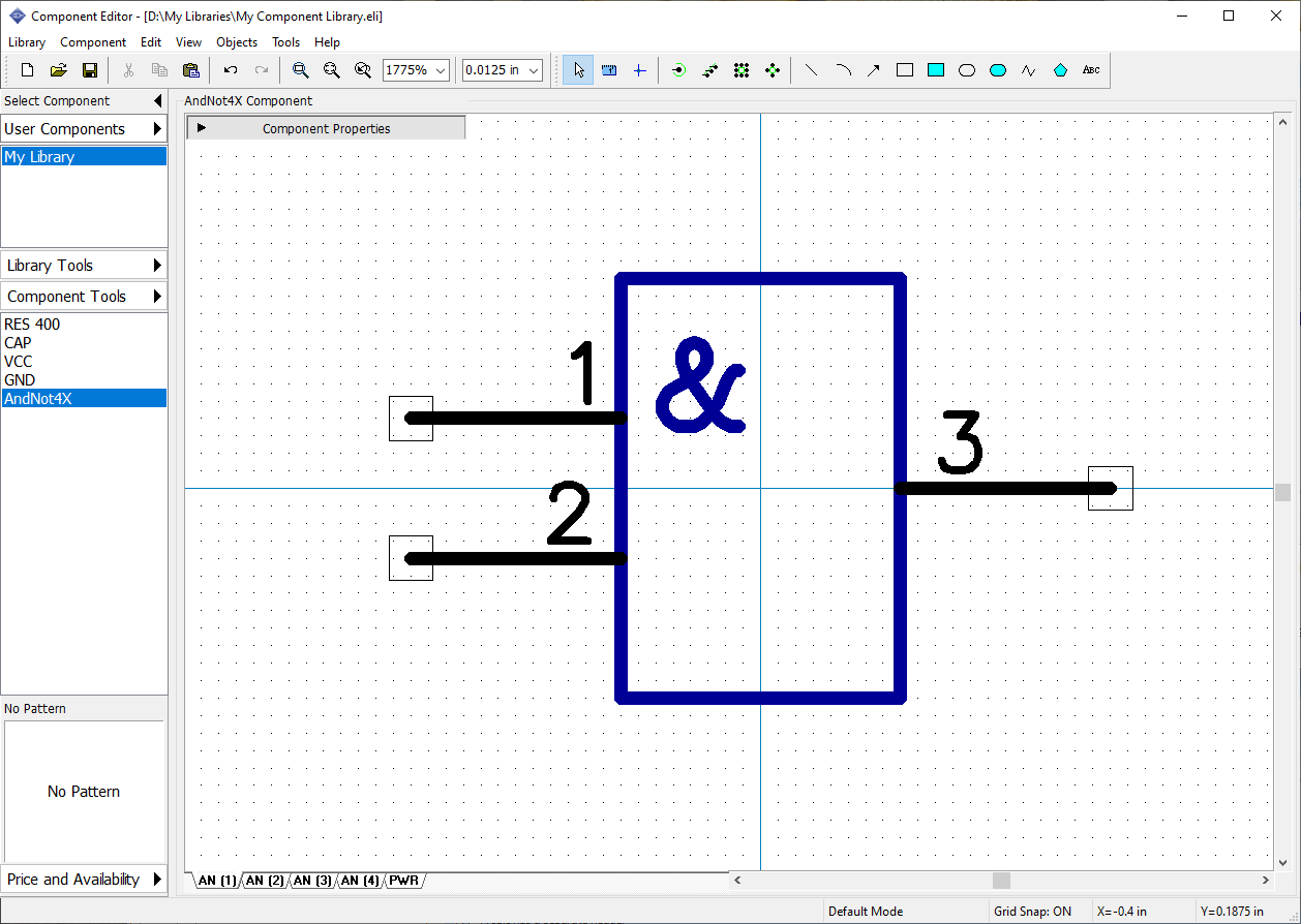
Right pin of a typical "And - Not" (Not And) part should be inverted or "Dot" type. Right-click on the third pin, select Pin Properties from the submenu, in the pop-up dialog box specify Type: Dot. Click OK to apply changes and close the dialog box.
Notice that you don’t need to draw another AN parts of the component if they were created as a group of similar parts, they will inherit the layout of the first part of the "AN" group.
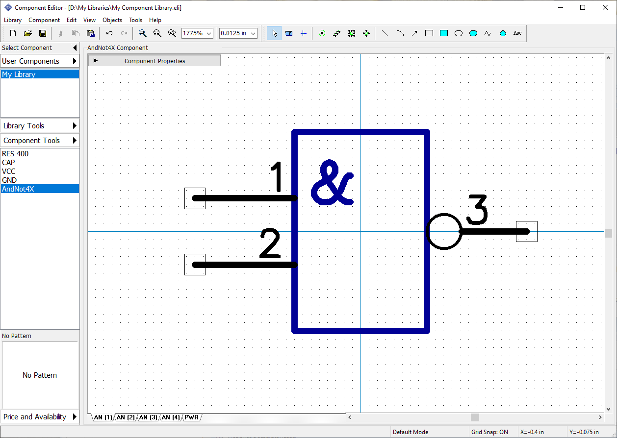
Select AN (3) or AN (4) part just to make sure that parts are the same. All parts in the group are absolutely identical, but require pin renumbering.
Pin Manager
Select "Component / Pin Manager" from the main menu. In the Pin Manager dialog box select part (using the drop-down list in the upper-right), define pin numbers, then select next part and so on, until you define pin numbers for all AN parts. Use the Down arrow button or Enter to quickly switch to the next pin when you're typing in the Number or Name fields.
Don't forget that pin #7 is used in the GND part, therefore you should skip it while renumbering pins of the functional parts, going from pin #6 straight to the pin #8. Also note that starting from pin #8, the output pin number is lower than the input pin numbers.
Please set correct Electric type (2 input pins and one output pin) for one of the parts and the other parts will inherit this automatically. Click OK.
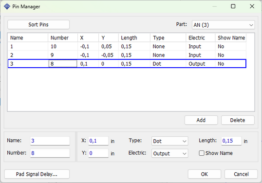
The next step is attaching a related pattern to the multi-part component. Press the Pattern button on the Component Properties panel. In the Attached pattern dialog box select the Patterns library group (library group with all standard pattern libraries), then select DIP Pitch 2.54mm library and DIP793W45P254L1955H393Q14 pattern in there (use filters if you like).
Notice that you don’t need to specify pin-to-pad connections, they have been assigned automatically and should be correct, because we've specified correct pin numbers in the Pin Manager (this is why pin number array was not straight).
Select different parts (drop-down list below the preview field) and visually check connections to ensure that they are all right. Press OK to attach pattern and close this dialog box.
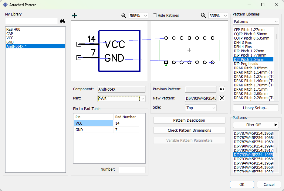
Multi-part component is ready. Save the library file.
47. Using additional fields
Name, RefDes, Value, Manufacturer, and Datasheet are default component fields in the DipTrace, usually, these are what most users will ever need, but sometimes additional description or other information is necessary. In this case, you can use additional fields.
Select "Component / Default Additional Fields" from the main menu. This dialog box allows you to specify default additional fields and their values. For example, we need to have the link for one more datasheet online: type in "Datasheet #2" into the Name box, specify Type: Link, enter the web address, and click Add button. Now this additional field will apply only to all new components that you will create. If you want to add this additional field to all existing and future components in this library, then press the Add to All button.
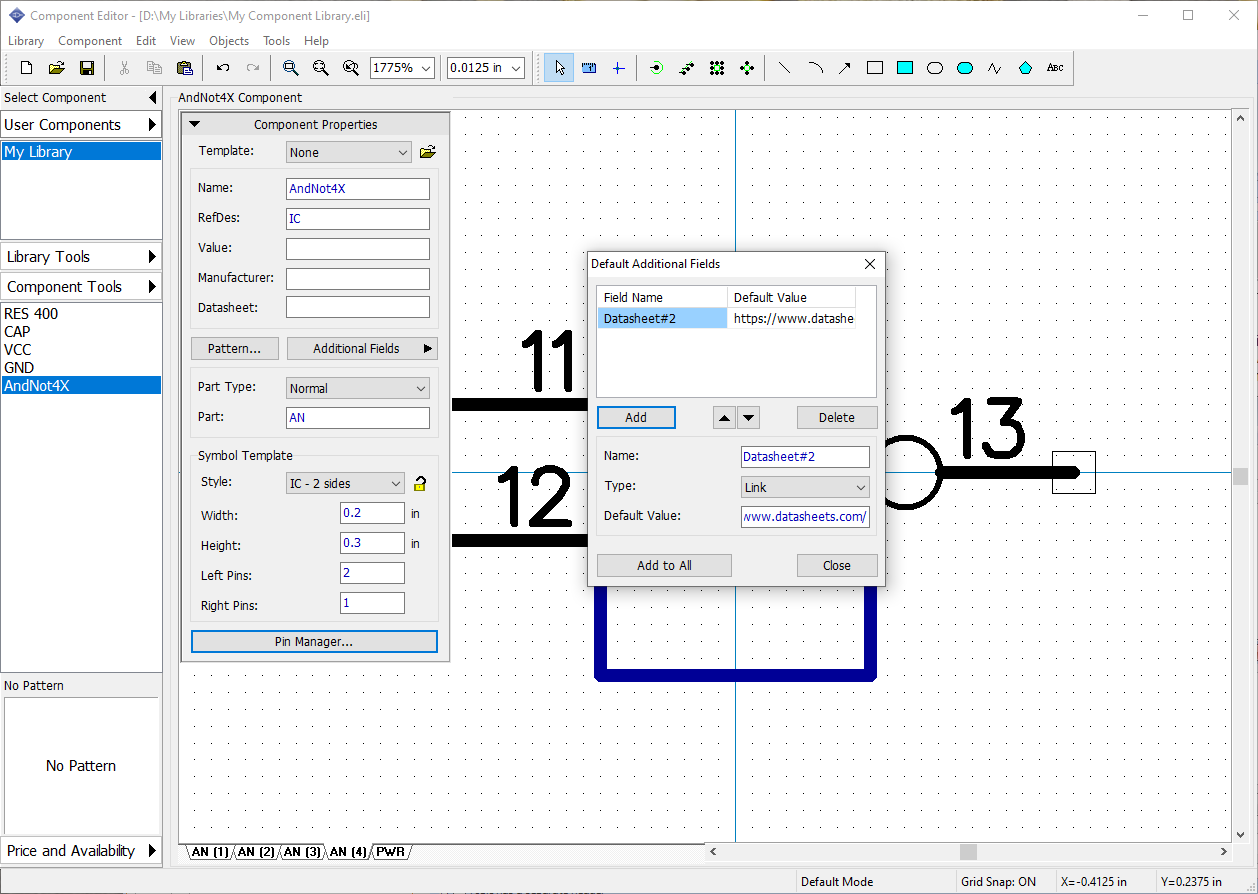
Now all components in this library will have this additional field with the datasheet link. Close Default Additional Fields dialog box. Select , then select Add New Component to "My Library" or press Ctrl+Ins. Click Additional fields button to see the list of all additional fields for a new component.
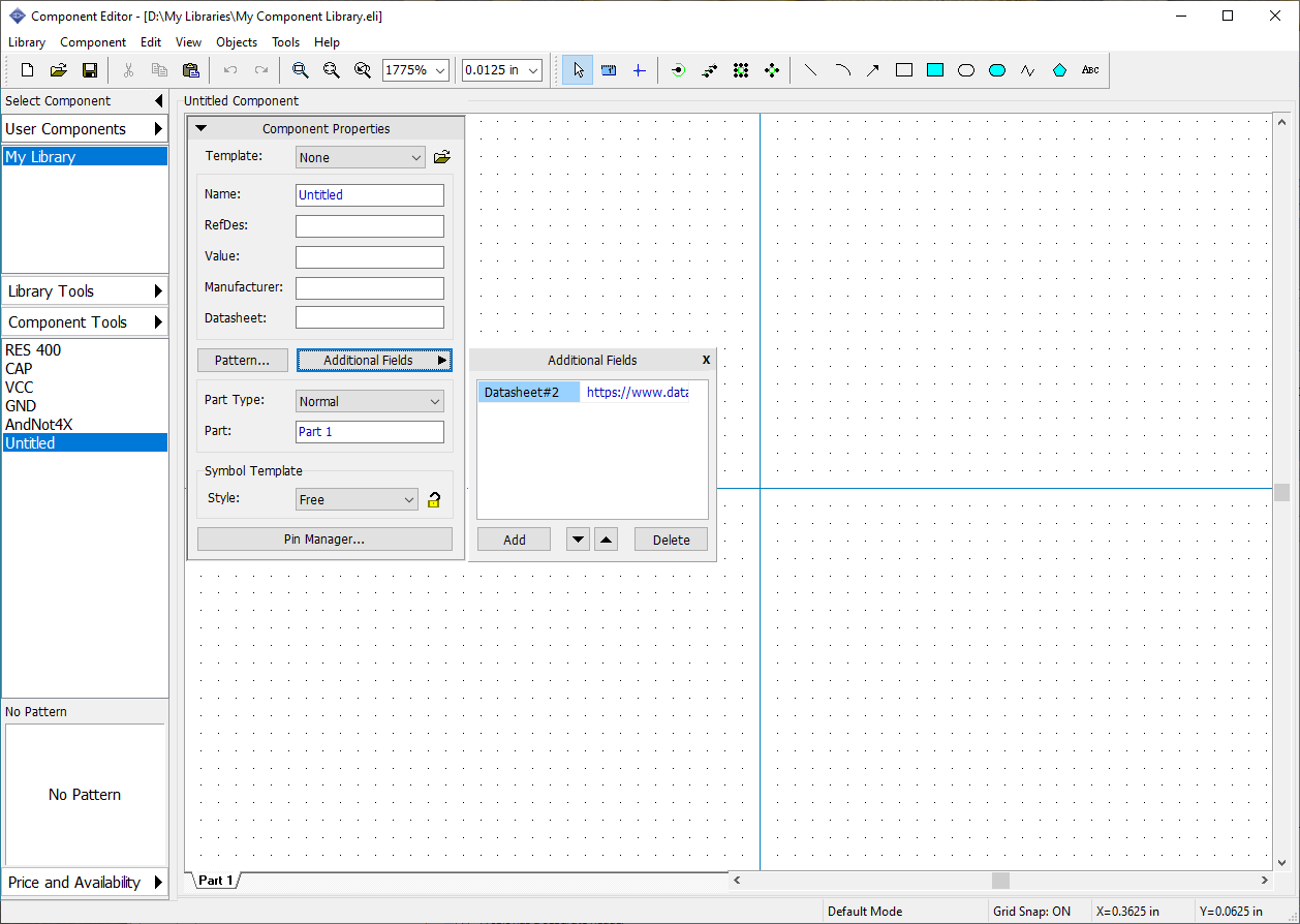
It has the added Datasheet field.
Now make sure that Untitled component is selected on the Library Manager panel, right-click it, and select Delete Components or simply press Ctrl+Del to delete it. You can also select several components and delete them at a time.
You can assign custom additional fields to the component, just press the Additional Fields button on the Component Properties panel and practice a bit.
Additional fields in Schematic
Right-click on the component with links to the datasheets on the design area in DipTrace Schematic, and select Links from the right-click submenu, the web browser will pop up automatically. You can assign additional fields as component markings for all or only for selected components in the DipTrace Schematic.
Advanced component modeling
48. Designing PIC18F24K20
In this part of the Tutorial we will create a PIC18F24K20 component according to the datasheet and attach SOIC-28 pattern that was created before.
Go to the Microchip website and search "PIC18F24K20", then select "Download datasheet". Or use the direct link (however we don't guarantee that it works at the moment you read this tutorial). Go to "Pin Diagrams", the first diagram is what we need.
In the DipTrace Component Editor and add a new component (Ctrl+Insert), type in the name "PIC18F24K20", RefDes and manufacturer, then specify Style: IC - 2 sides, Left Pins: 14, Right Pins: 14.
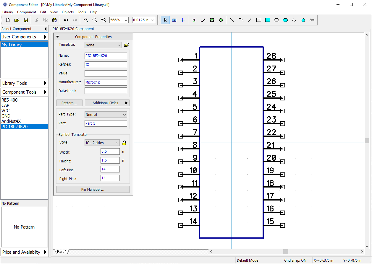
DipTrace allows the user to enter pin names manually or import them from external BSDL file ("Library / Import / BSDL Pinlist" from the main menu). You can also import pin lists (parts, pin names/numbers) from CSV and TXT files ("Library / Import / Pinlist" from the main menu). We will do this manually. Press the Pin Manager button on the Component Properties panel and enter pin names from the pin diagram in the datasheet found online. Notice that you can resize the pin manager panel and change the width of the columns (we made the Name column wider to see the full pin names). Also when you entered the pin name, just press Enter to switch to the next pin name easily.
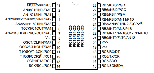
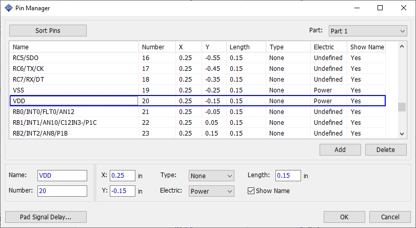
After entering all pin names, specify electric types for pins, and check the Show Name box for all pins of the component. Notice that you can select as many rows as you need and change certain properties at a time. Press OK.
Our symbol has inappropriate look, width is too small with pin names overlaying.
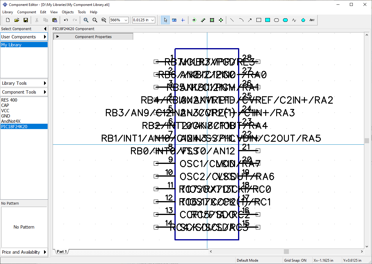
On the Component Properties panel change width to 1.9 inches and height to 2 inches. Pin names still overlay a bit, but we will regroup pins which will probably fix this. We made an IC a bit bigger because it will make it easier to do the pin regrouping. Change grid to 0.1 inch and place pins by this grid (select all pins, right-click, and select Snap to Grid from the submenu).
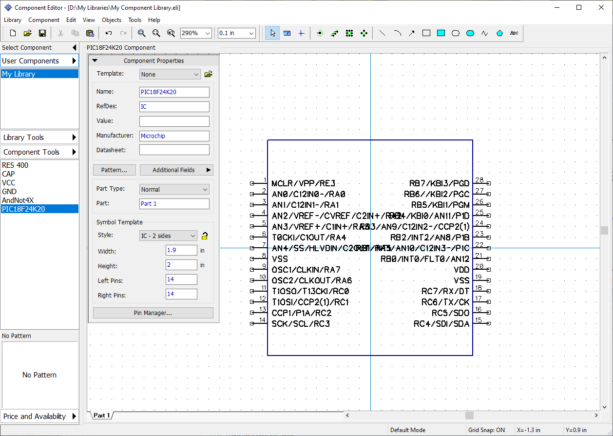
Make buses (Group pins)
We need to group pins logically. First, we will make the busses – select "Component / Make Buses from Pins" from the main menu. This feature allows the user to extract buses based on the pin names and group pins by buses. In the pop-up dialog box, you can define possible bus dividers. By default, only "/" is selected and it is OK for the current component, however, some manufacturers use different dividers.
Press Extract button and you will see available buses and number of pins for each of them. Select RA, RB, and RC buses using Ctrl key. Change Bus to Bus spacing to 1.3 inches, because pin names are quite long.
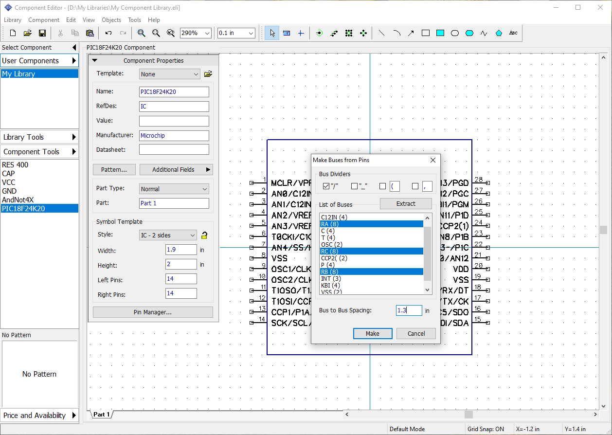
Press Make button to make the buses and close the dialog box. DipTrace sorts wires by buses to the left from the IC symbol.
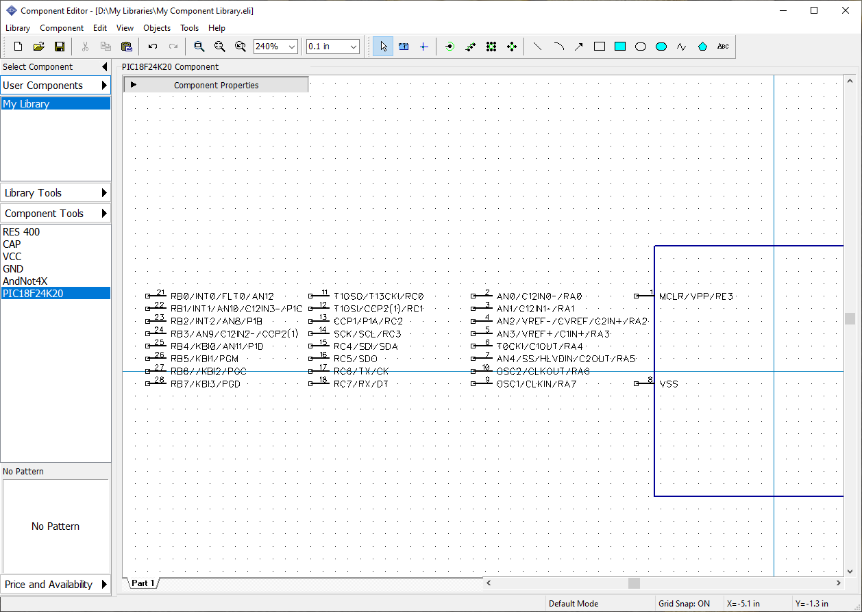
There are some pins that do not belong to the selected buses (4 pins left on the symbol). Select them, use Ctrl and box selection, then move pins away from the symbol, for example, to the bottom, because we need to place the busses first.
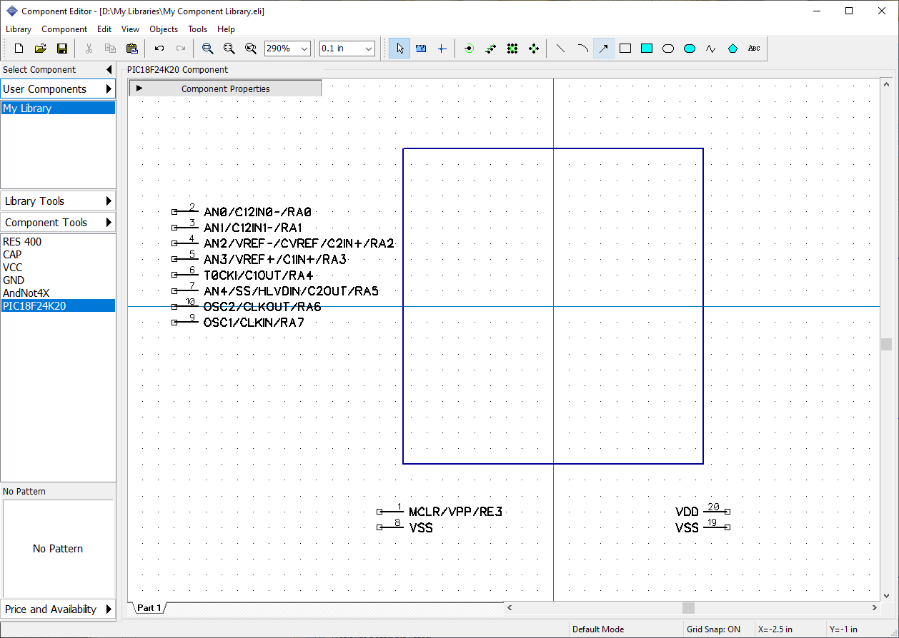
Place buses to the IC rectangle like in the picture below. Use box selection to select a bus, then drag it. Press Shift+R to rotate the bus and Shift+F to flip pins, or select these commands from the pin submenu (right-click on one of bus pins). Move the rest of pins to the IC rectangle (press R to rotate selected object/pin).
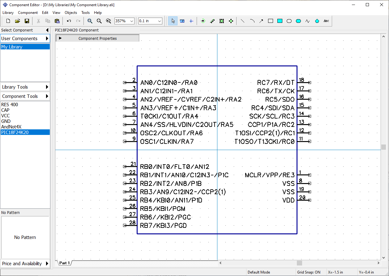
Sometimes you need to place pins by electric type, select "View / Pin Colors by EType" from the main menu and the software assigns different colors for pins of different electric types.
Press button on the Component Properties panel to lock properties.
The final step is attaching SOIC-28 pattern to the component. Press the Pattern button on the Component Properties panel and select SOIC-28 pattern from My library (we've created it before). Select your library group, then select My Library (Patterns) and SOIC-28 from the list below. All pin names and pin numbers are already there. You can check pin to pad connections in the table. We don't need to change anything. Just press OK.
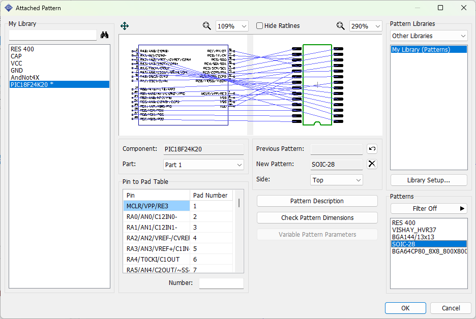
PIC18F24K20 component is ready! Save the library.
49. SPICE Model
With DipTrace you can export schematics into LT Spice to simulate it and see how the circuit works or use the built-in NGSPICE simulator. We will review the simulation step later, for now, we need to define correct SPICE model for the component, otherwise, the Spice simulation for this component will not work. Now we will specify that our CAP component is a capacitor with some value, so it will work in the SPICE netlist. Select CAP on the Library Manager, then select "Component / Spice Model" from the main menu. Set: Model Type: Capacitor, then double click in the Parameters table in the Value cell (the value reads "1uF" text) and enter a new value – "23 μF" (DipTrace supports Unicode characters). Press Enter or just move focus to another field.
In the Template field, you can see how this part looks in the SPICE netlist language. In our case, pin-to-signal map is correct, however, if you need to edit it, enter signal names into the table on the left side of the Spice Settings dialog box. The list of available signals is right below that table.
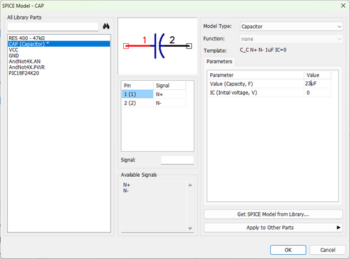
Capacitor is a very simple component, we don't need specific text file model to let the simulation software know how this component works (model type and capacity is just fine). However, for transistors, you can load models from external files (usually SPICE models are available on the manufacturers' websites) or enter model text manually if you know how to do that (see SPICE Language documentation for details). Also, there is a SubSkt Model Type, which allows the user to enter/load model of almost any part as a program.
Press Get Spice Model from Library button to load existing Spice settings from another DipTrace component.
Notice that this dialog box is also available in the Schematic Capture, you can define Spice settings after completing or while drawing the schematic.
Library design is ready. Click OK to apply changes and close the Spice settings. Save the library file.
Library verification and part placement
50. Library verification
It is very important to verify library for the most common types of errors. We've investigated the work of our library designers and added an automatic error verification to the Component Editor.
In the Component Editor select "Library / Check "My Library" Library" from the main menu. In this dialog box, you can see the total number of components/parts/pins in your library and all possible errors.
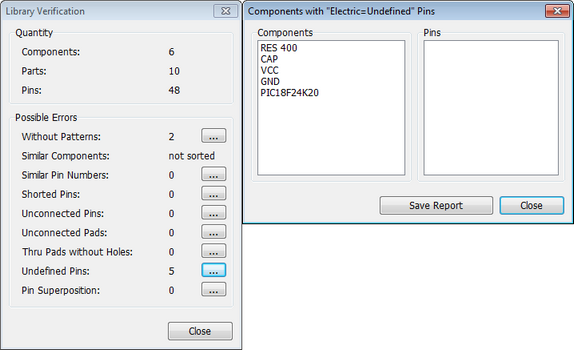
The following errors can be found automatically:
1. Components without patterns – search components without patterns. Keep in mind that some components may have only schematic symbol intentionally.
2. Similar components – search components with similar names. Notice that library should be sorted ("Library / Sort Components in <current library>" from the main menu) to enable correct verification.
3. Similar pin numbers – two or more pins have similar numbers (connected to the same pad). This is probably a mistake in the component, please press the button and check pin numbers for the listed component.
4. Shorted pins – pins are shorted by internal pad-to-pad connections.
5. Unconnected pins – pins do not have the corresponding pattern pads. It's not always an error.
6. Unconnected pads – some pads of the pattern are not used (no corresponding pins). It is not always an error.
7. Through pads without holes – verifies components for the through pads without a hole. In the majority of cases this is a mistake in SMD pattern, please check if pads do really have the surface type selected.
8. Undefined pins – some pins have "Undefined" electric property.
9. Pin superposition ― some pins superimpose on the symbol, in the majority of cases this is a mistake made while placing the pins.
To see details (list of components and pins) press button next to the corresponding mistake. You can save the list of errors can as a text file.
Save changes and close the Component Editor.
51. Placing parts
Schematic
Open the Schematic module, i.e. go to "Start / All Programs / DipTrace / Schematic" in the Windows OS or use the DipTrace Launcher if working on MacOS. Select My Library from the User Libraries library group. Place a couple of resistors and capacitors to the design area. Just left-click on the component on the Place Component panel and left-click on the design area. If the origin is shown, press F1 to hide it. Usually, you don't need the origin point for designing schematic.
Notice that you can place components using "Objects / Place Component" dialog box or with the  button on the Objects toolbar.
Notice that the colors of components, selections, etc., depend on the color template and user preferences.
Multi-part component placement
|
Select multipart component (AndNot4X). DipTrace always shows that the current component is multi-part or a net port in the symbol preview field on the Place Component panel (<the number of parts> or "Net Port" text). We have created AndNot 4X with four similar parts and a power part. You can place all parts as a single item or each part separately, use the Select AN(4), leave Auto PWR/GND checked, and place AndNot4X component part by part. DipTrace automatically selects the next part from the part group and places the power symbol for the component. |
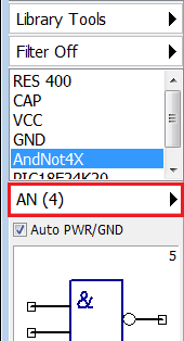

Notice that program will automatically switch to the next part when all parts had been placed. Make sure you place parts only with RefDes from 1.1 to 1.4, like in the picture below.
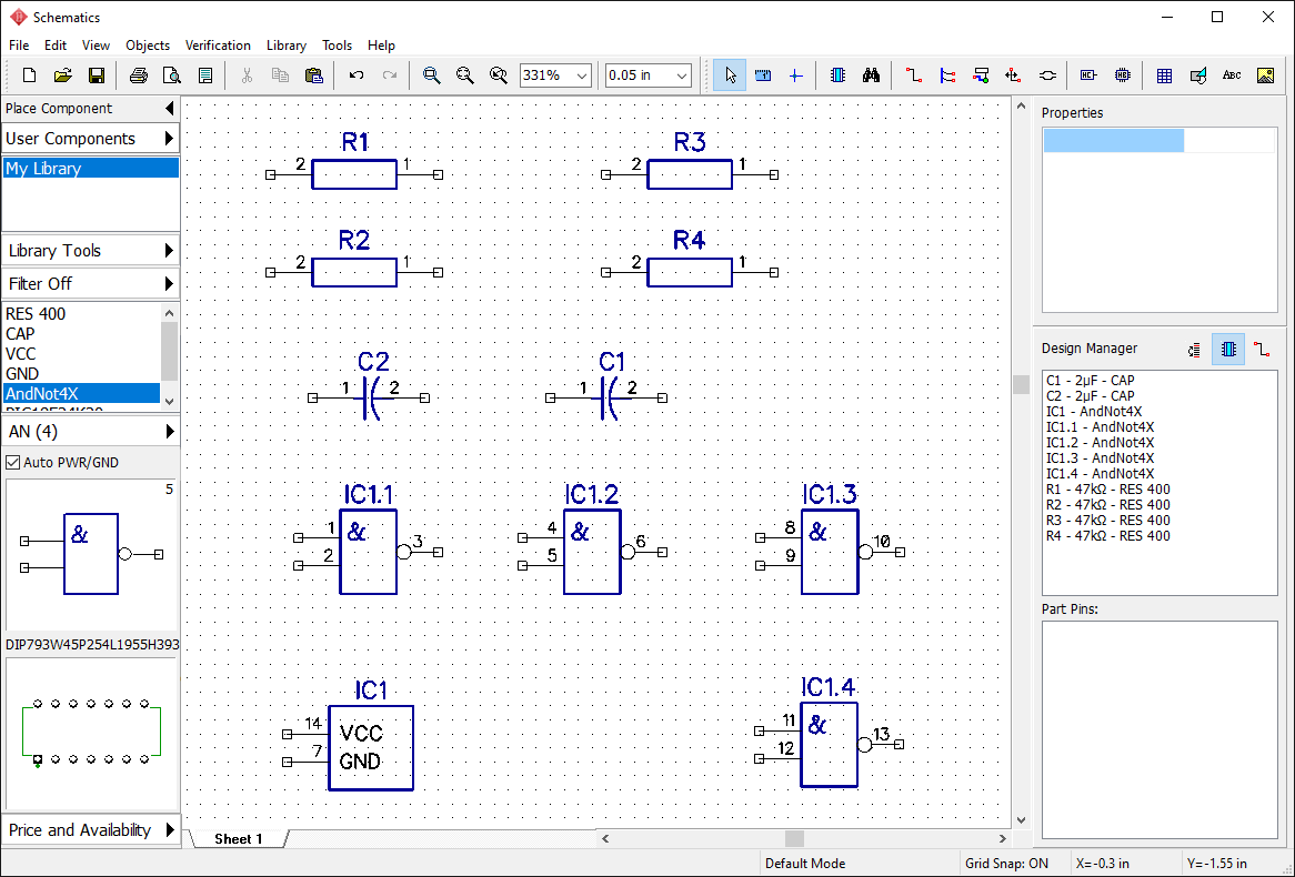
|
As you can see the similar parts of the multipart component are already grouped inside the part selection drop-down list. Deactivate "View / Group Similar Parts" item in the main menu to ungroup parts. If this item is checked, all logic parts of the component (AN(4) in this case) will be grouped inside the All Parts pop-up menu. If unchecked, you will be able to select and place each AN part separately. |
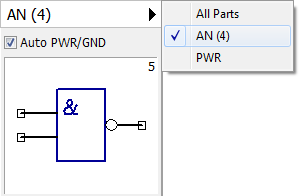
Connection via net ports
Net Ports are single-part components used to establish connection between nets without
wires. DipTrace Standard Libraries contain all the most popular net ports, but you can
also create new ones in the Component Editor. Net Port components have no patterns
attached since these elements are used only in Schematic to connect wires without visual
connections, and do not exist on the circuit board. Net ports are usually applied to Ground
or Power nets and schematics with flexible structure.
Let's practice using Net Ports. Make sure that you have two complete AndNot components on the design area (IC1 and IC2) with two power symbols. Now we'll try using the net ports. Select VCC and GND net port symbols from the library, and place two of each to the schematic. Connect pins like in the picture below.
Notice that two wires connected to the same pins of the same-type net port are connected to a single net automatically.
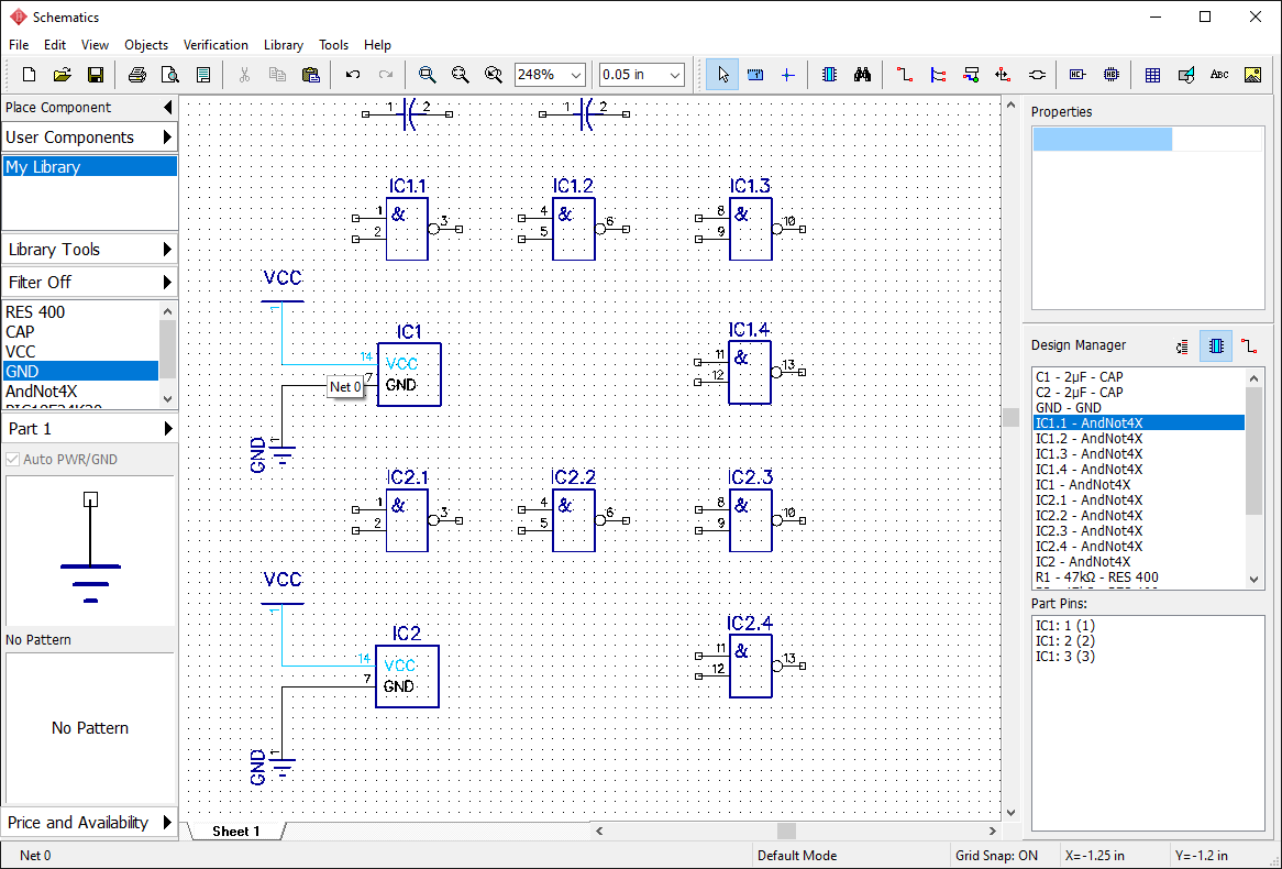
To rename net which connects VCC pins, right-click on the wire, and select the first item from the submenu or right-click on the pin, and select the Net Name.
Notice that you can change part names directly in Schematic (on the Component Properties dialog box).
Schematic allows the user to:
1) Connect pins to nets without wires (right-click on the pin, select Add to Net, then select net, check Connect without wire, and press OK);
2) Merge nets by name (check Connect Nets by Name check box in the Net Properties dialog box);
3) Connect pins to the net with similar name automatically (check Connect Net to Pins by Name checkbox in the Net Properties dialog box). The last method is the fastest way to connect VCC, GND (if you plan to hide power nets and parts), CLK, etc. More information later in this tutorial. Close the Schematic. Do not save the changes.
PCB Layout
Open DipTrace PCB Layout module, i.e., go to "Start / All Programs / DipTrace / PCB Layout" on Windows or use the DipTrace Launcher on MacOS.
As you already know, correct component always includes at least a schematic symbol (for Schematic) and attached pattern (for PCB Layout). Schematic works only with symbols, while PCB Layout allows to select component libraries and place component's patterns on the board. If you have selected component library and there are components without attached patterns, you can not place them on the board. Notice that there is the Patterns library group for convenience, which allows the user to place patterns as separate entities (no schematic symbols attached).
Select User Patterns library group and My Libraries (Patterns) library. You will see that all the patterns that we have created during the lessons of this tutorial are available here. Now select My Library from the User Components library group. As you remember, we did not attach patterns only to net ports, therefore we can not place them on the circuit board in the PCB Layout. All other components work just fine because they all have attached patterns.
Place some components of the library to the design area, excluding the VCC and GND (select component on the Place Component panel and left-click on the design area to place it), then return to My Library (Patterns) from the User Patterns library group and place BGA-144/13x13 pattern, which we did not attach to any of the symbols, therefore it is not available in the component library.
Change common marking settings to show RefDes and Name ("View / Component Markings; in Show column check RefDes and Name; Align - Auto). For individual customizations, right-click on the component, select Properties, select the Markings tab.
Select Bottom Side in the drop-down list on the Objects toolbar if you want to place components on the opposite side of the board. For existing components, you can change side with the right-click submenu. For example, the R3 resistor is on the bottom side (see the picture below).
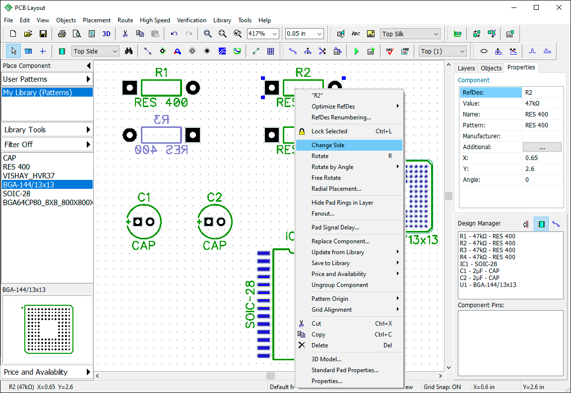
You can change pad properties for a separate pad or entire pattern directly in the PCB Layout. Let's change one of the resistor pads. Hover over the pad you want to change (it should be highlighted), right-click it, and select Pad Properties from the submenu. In the pop-up dialog box uncheck the Use Pattern's Standard Pad Properties checkbox for custom pad settings or press Pattern's Standard Pad Properties button to change default pad settings for the pattern. To edit pattern pad properties, right-click on a pattern (not a pad) and select Standard Pad Properties from the submenu.
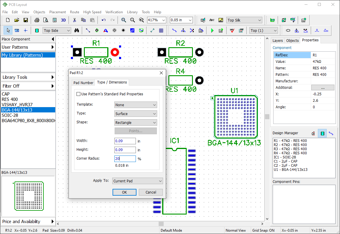
Notice that if pattern's origin is different from the pattern's center position, the software will show it while placing that pattern.
You can show/hide the pattern origin for all selected components: right-click one of them, and select Pattern Origin from the submenu. Try to rotate different components and you will see that the pattern origin is actually the center of rotation. When hovering over the pattern you will see the coordinates of the pattern, which are actually the coordinates of the pattern's origin.
52. Other features and tools
This part of the tutorial includes the description of important DipTrace features not reviewed above. We consider that the reader already knows how to accomplish basic tasks in DipTrace. Therefore, we can move on to more complex stuff.
Connecting
Schematic connections
53. Buses and bus connectors
Now we'll learn how to use buses and connect sheets with bus connectors in the Schematic. You can work with the circuit from the previous subsection of this tutorial or create a new schematic with random components for practicing.
Create a bus
Select "Objects / Circuit / Place Bus" from the main menu or press  button on the Objects toolbar, then draw a bus line on the design area by defining its key points. Right-click, and select Enter to finish bus placement. Right-click on a free space to switch to the Default mode. Hover over some pin with the mouse, left-click it, and move the mouse pointer to the bus, and left-click again to create a wire.
In the pop-up dialog box, you can define a name of a new net or connect a wire to one of existing nets (which are already connected to that bus).
We did not connect the wire to the existing net. This is why we have seven separate wires-nets (Net 0 – Net 6) not connected to each other via the bus. Fortunately, you can change the wire-to-bus connections at any moment, just move the mouse cursor to the wire segment connected to the bus, right-click, and select Bus Connection from the submenu.
In the pop-up dialog box connect Net 6 to Net 2 (select Net 2 from the list of the bus wires). Now there is no Net 6 anymore. We have a single Net 2 connected via the bus.
Add a new sheet to the schematic, select "Edit / Add Sheet" from the main menu or press Ctrl+Ins hotkeys. You can see the list of sheets as tabs at the bottom-left corner of the design area. Select Sheet 2. The multi-sheet and hierarchical structure is described later in the corresponding section of this tutorial.
You can rename, move, delete, or insert new schematic sheets, right-click on the sheet in bottom-left of the design area and select appropriate action from the submenu.
Bus connector
Press  button on the Objects toolbar and place a bus connector on the Sheet 2 (it should have "Port 0" name), then select Sheet 1, and place one more bus connector there (it will be named "Port 1" automatically). Now connect the existing bus to the Port 1 connector: select the bus tool, left-click on the bus and draw the line to the bus connector (blue circle in the center of the connector) and left-click it to finalize.
Notice that bus connector glows green if the bus is properly connected to it, blue circle means that there is no connection.
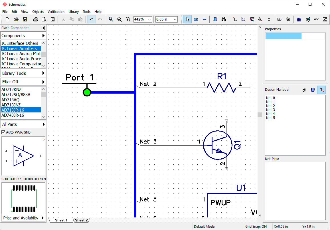
Notice that two bus connectors on different sheets are still unconnected (they should have the same name in order to be connected).
Rename Port 1, hover over it with the mouse cursor, right-click it, select the first item from the submenu, and rename bus connector to "Port 0" (as you remember we've placed "Port 0" on the Sheet 2). Press OK. You can see that the a has appeared around the port's name. That means that this bus connector is connected to another bus connector. In our case, the connector from the Sheet 1 is connected to the connector on the Sheet 2.
Notice that designer can connect more than two bus connectors by defining the same names to all of them.
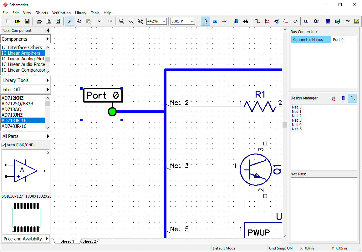
Select Sheet 2, and create a bus connected to the Port 0.
Notice that the name of the bus on this sheet is the same as on the first sheet, i.e. this is a common bus. Now you can place random electronic components on the second sheet (for example AD1856RZ from IC Data Acq DAC library) and connect their pins to the nets on the first sheet via the bus.
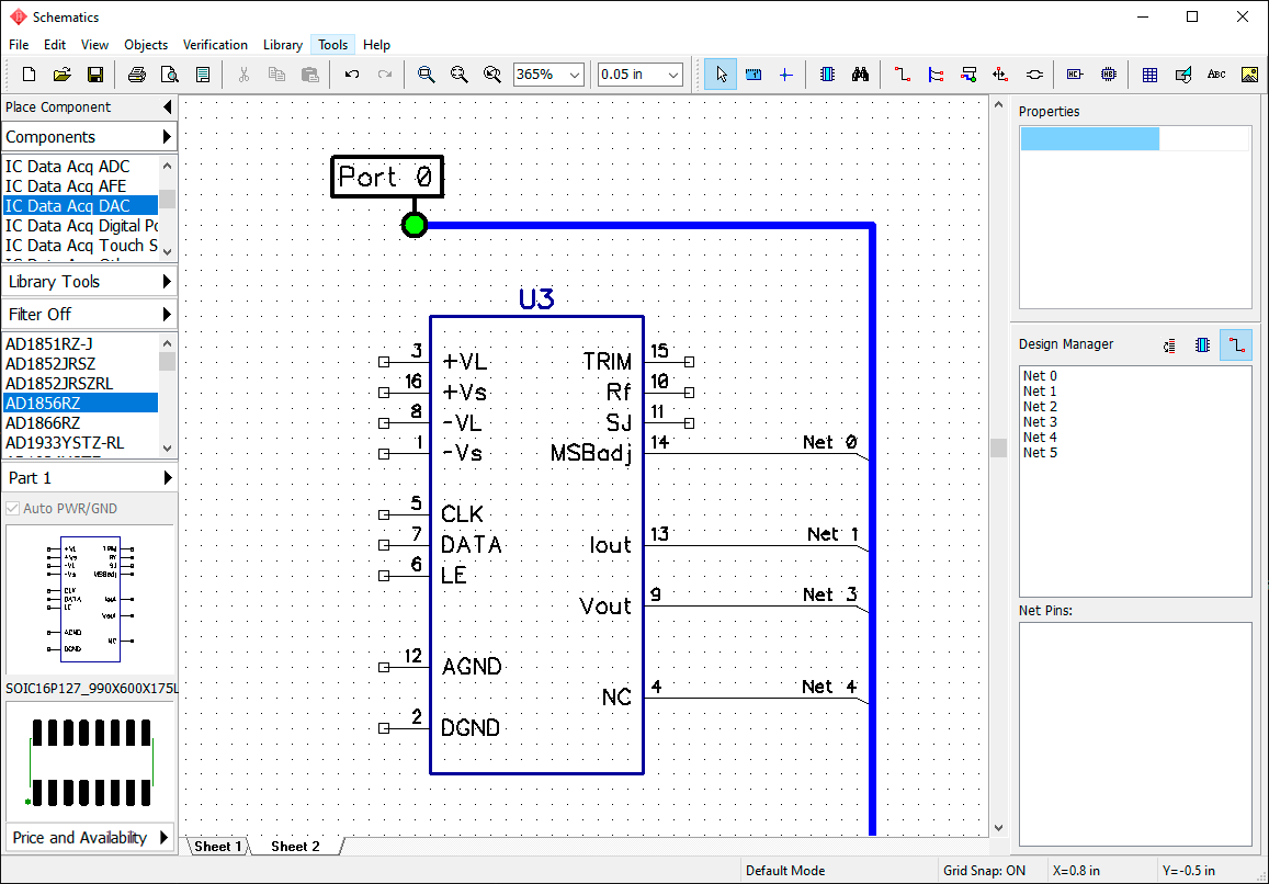
54. Net ports
We tried using single-pin net ports before in order to create VCC and GND connections. This is the most common application of such components in real life, but sometimes multi-pin net port is a more comfortable design solution.
Make sure there are unconnected pins on the Sheet 2. Select the Net Ports library from the Components library group on the Place Component panel, find Bus_Port_Out 8 component, and place it on the design area.
You can change the displayed net port marking in its Properties on the Part Markings tab from the context menu. These settings will also be applied to subsequently placed net ports.
Make connections from the component pins to the pins of the Bus Port, then position Bus_Port_Out8 component on the Sheet 1, and connect some nets to it. Notice that net names connected to the same pins of Bus Port 8 on Sheet 1 and Sheet 2 are the same, i.e. all wires connected to pin 1 of the Bus_Port 8 are connected to a single net, the same with other pins. You can connect or disconnect ports (i.e. change schematic structure) by renaming them.
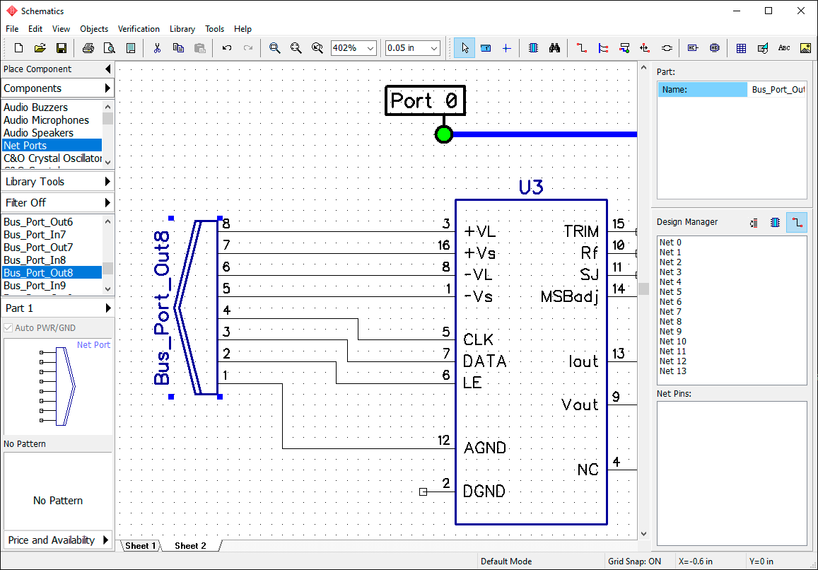
55. Connecting without wires
As you already know, DipTrace allows the user to connect pins visually (wires, buses) and logically (without wires, by name, with net ports).
Connecting pins without wires
You can connect pins logically without wires. In this case, pins do not depend on the sheet or part location.
Hover over an unconnected pin with the mouse, right-click it, and select Add to Net from the submenu. In the pop-up dialog box select a net from the drop-down list, and check Connect without Wire checkbox, then press OK. In the picture below you can see two pins connected without wires.
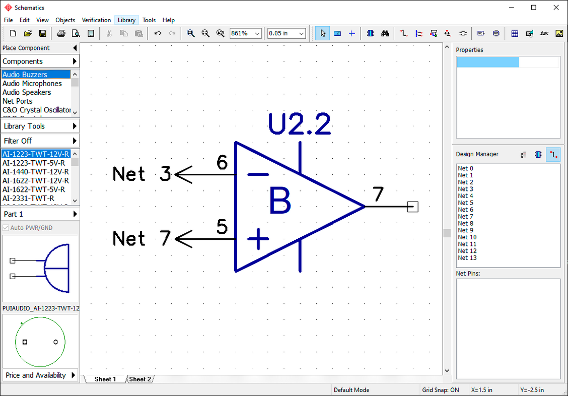
Connecting pins by name
Now find a blank spot on the design area where we will try to connect pins to a net by name. Place a single GND symbol from the Net Ports library, and create a small wire from the GND's pin. Move the mouse a bit upwards, and press Enter, like in the picture below, to create a wire segment. Now right-click on the wire segment connected to the GND net port, and select Properties from the submenu.
In the Net Properties dialog box rename net to "GND," and check Connect Net to Pins by Name checkbox. Press OK to apply changes.
DipTrace automatically connects all unconnected pins with the corresponding name to this net.
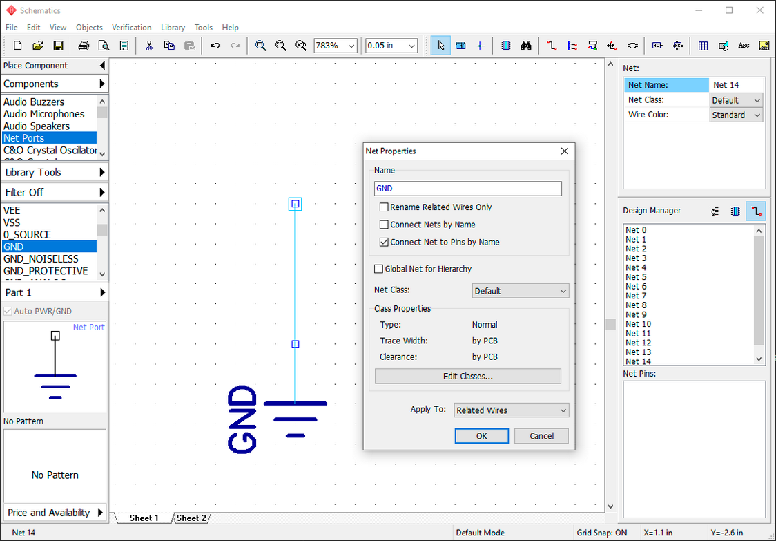
Select IC Data Acq DAC library, and find AD420AR-32 component (press  button, type "AD420AR-32" into the name field and press Apply Filter). Place several AD420AR-32 components on the design area.
Notice that all GND pins of the placed components are automatically connected to the GND net without wires due to active Connect Net to Pins option in the Net Properties dialog box. This feature is the easiest way to connect pins with the same names for the entire schematic. Usually applied to POWER, GND, CLK pins or even data buses.
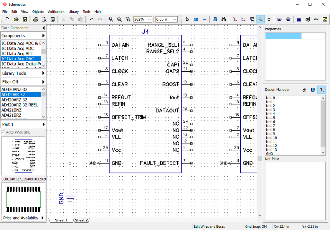
Connect nets by name
DipTrace allows the user to connect nets on different sheets without net ports or buses. Remember the name of some net that you have on the first sheet (for example, Net 3), then go to Sheet 2, and right-click on the net you want to connect to Net 3. Then select Properties from the submenu, type in "Net 3", check Connect Nets by Name checkbox, and press OK.
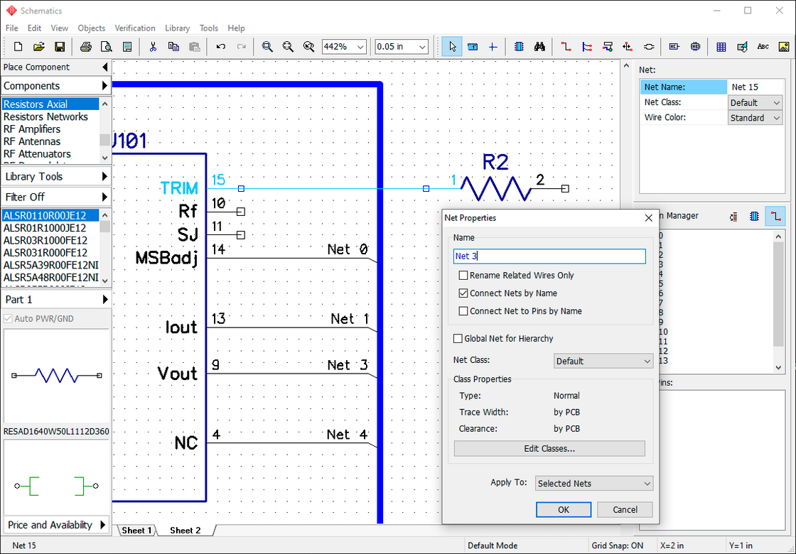
This feature works like a regular net renaming. When you enter the net name that already exists anywhere on the schematic, DipTrace asks if you want to connect these nets by name.
Notice that you can not connect nets by name on different levels of hierarchy.
For hierarchy, you can create global nets. We will learn how to use them later in the Hierarchical Schematic topic of this tutorial.
56. Connection Manager in Schematic and PCB Layout
Connection Manager is another DipTrace tool which allows the user to create/edit/delete connections in Schematic and PCB Layout. Select "Objects / Connection Manager" from the main menu in Schematic or "Route/ Connection Manager" in the PCB Layout.
|
Open connection manager in Schematic. Select a net from the drop-down list, and you'll see all pins of the selected net. You can easily add/delete pins to/from the net. To add new pins to the net, select a component and its pin with the corresponding drop-down lists, and press Add button. Notice that only unconnected pins are available in these drop-down menus, so if you can not find a pin that you need, it is probably already connected to another net. Use Press OK to apply changes and close the Connection Manager or press Cancel to close it and maintain the net structure unchanged. |
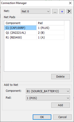


Components and layout preparation
57. Looking up components
DipTrace 4.X includes 170,000+ components in the standard libraries, and we continuously expand them. Components are sorted by types. The cross-module library management system with custom library groups and search filters allows the user to seek through the libraries and quickly find what he needs.
Search filters
Go to "Objects / Find Component" from the main menu in the Schematic or press  button on the Place Component panel to customize the search filters.
|
In the pop-up dialog box specify the search area: All Libraries, current library group or current library, and type in the name or part of the name of the component. DipTrace allows for filtering components by Keyword, Name, Value, Pattern, Manufacturer, Datasheet or Additional Fields. Press |
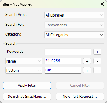
As you can see in the picture, we search for 24LC256 memory in a DIP package.
Press Apply Filter. You can stop the search at any moment by pressing Stop Filter button. As soon as the search is completed, only filtered components that correspond to the search filters are visible on the Place Component panel. The state of the search filters is always displayed on the Place Component panel – "Filter ON/OFF." To disable the search filters, open the search filters dialog box, and press Cancel Filter.
You can redirect the search with the entered parameters to SnapMagic database by pressing Search at SnapMagic button (see detailed description below).
If some component is not available neither in the standard libraries nor in SnapMagic database, you can press New Part Request button to place an order for its design by DipTrace engineering team.
Place component
You can find and place components with the Place Component dialog box ("Objects/ Place Component" from the main menu in Schematic). There are two sections in the pop-up dialog box: Libraries and Components. Select library group from the drop-down list, then select a library, and, finally, select component from the corresponding list. Press Filter ON/OFF button to customize and apply the search filters.
"Objects / Place Component" dialog box is similar in the PCB Layout.
For example, we need a component that contains "232" in its name, but we do not remember the other characters, letters or even a possible library. Press Filter ON/OFF button, select Search area: All Libraries, type in "232" in the Name field of the filters dialog box, and press Apply Filter. DipTrace has found 500 components with "232" in their name. Components are in the list right below. Select a component, now you see its schematic symbol, press Display Pattern to see its associated footprint.
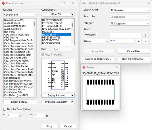
Add more search filters to narrow the results. Press Search at SnapMagic button redirect the search with the entered parameters to SnapMagic database.
Press the "Price and Availability" button to check the price and availability of the selected component from a featured supplier or all suppliers from the Suppliers Databases.
Press Place button and left-click on the design area to place the selected component or check Place by Coordinates checkbox and enter exact coordinates, where you want that component. This dialog box has all necessary tools to work with multi-part components as well.
SnapMagic database
DipTrace features and integrated tool that allows searching SnapMagic CAD database in all the modules. To launch the search dialog in PCB Layout go to Objects/ Search Parts at SnapMagic. Register a free account with SnapMagic - and you are ready to go. Let's look up an amplifier; enter LM358 in the Search line and press  . Select LM358D component from the results list.
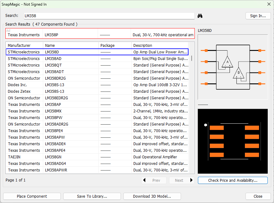
To select the most adequate component for the project, it is also useful to know its current availability and price. Press the "Check Price and Availability" button — you will be offered to consult the Mouser website or check all suppliers from the Suppliers Databases.
Now press Place Component button to place the pattern to your design. Alternatively, you can press Save to Library button to save it to an existing user library or create a new one. Remember that you cannot change standard libraries, so make sure to select a user library on the Place Component panel before saving the component.
Note that Download 3D Model button is active, which means that a 3D model for this component is available in the database. Press it and save a .step file to your computer. 3D model is attached to the component automatically, however, it's recommended to check its position relative to the footprint and map it, if necessary.
58. Reference Designators
Now we'll work with schematic examples located in the "Documents/ DipTrace/ Examples" folder. Open Schematic_2.dch file.
This project demonstrates application of various DipTrace features. However, we will experiment with some basic principles of working with Reference Designators in the Schematic.
This Schematic contains 23 capacitors from C1 to C24 (C19 is missing).
Optimize RefDes
While editing a principal circuit, sometimes you need to insert or delete components. Let's add a capacitor to the schematic, select HAK222KBACRBKR component from Capacitors Ceramic Disk library and place it on the design area. We want "C5" RefDes for this component, but the software automatically assigned the "C19" RefDes, because C19 was missing and C5 existed on the schematic. Change the RefDes: right-click on this capacitor, and select the first item from the submenu, enter "C5", and press OK. The warning message suggests to rename the component and shift the RefDes numeration, press Yes.
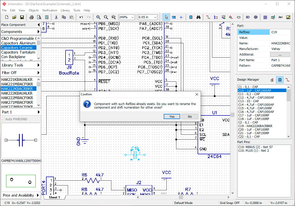
The C19 capacitor is now C5 and the old C5 became C6 and so on till C18 capacitor which is C19 now. See the design manager panel to the right to find out that C19 reference designator is not missing anymore because you have inserted C5 and C5 – C18 RefDes indexes were shifted ( use  button to sort the components in the list). Now we have the correct array of RefDes indexes for all capacitors.
Now rename the C5 capacitor to C30, then check the list of capacitor designators on the Design Manager (Ctrl+2 to show/hide the Design Manager, press button to sort the components in the list) – C5 and capacitors with C25 till C29 indexes are missing. To correct this issue, right-click on any capacitor, and select Optimize RefDes, then select RefDes "C" – C30 becomes C24. The reason is simple – while optimizing the RefDes, DipTrace removes all empty places in the designator index array. Therefore C6–C24 become C5–C23, and C30 becomes C24.
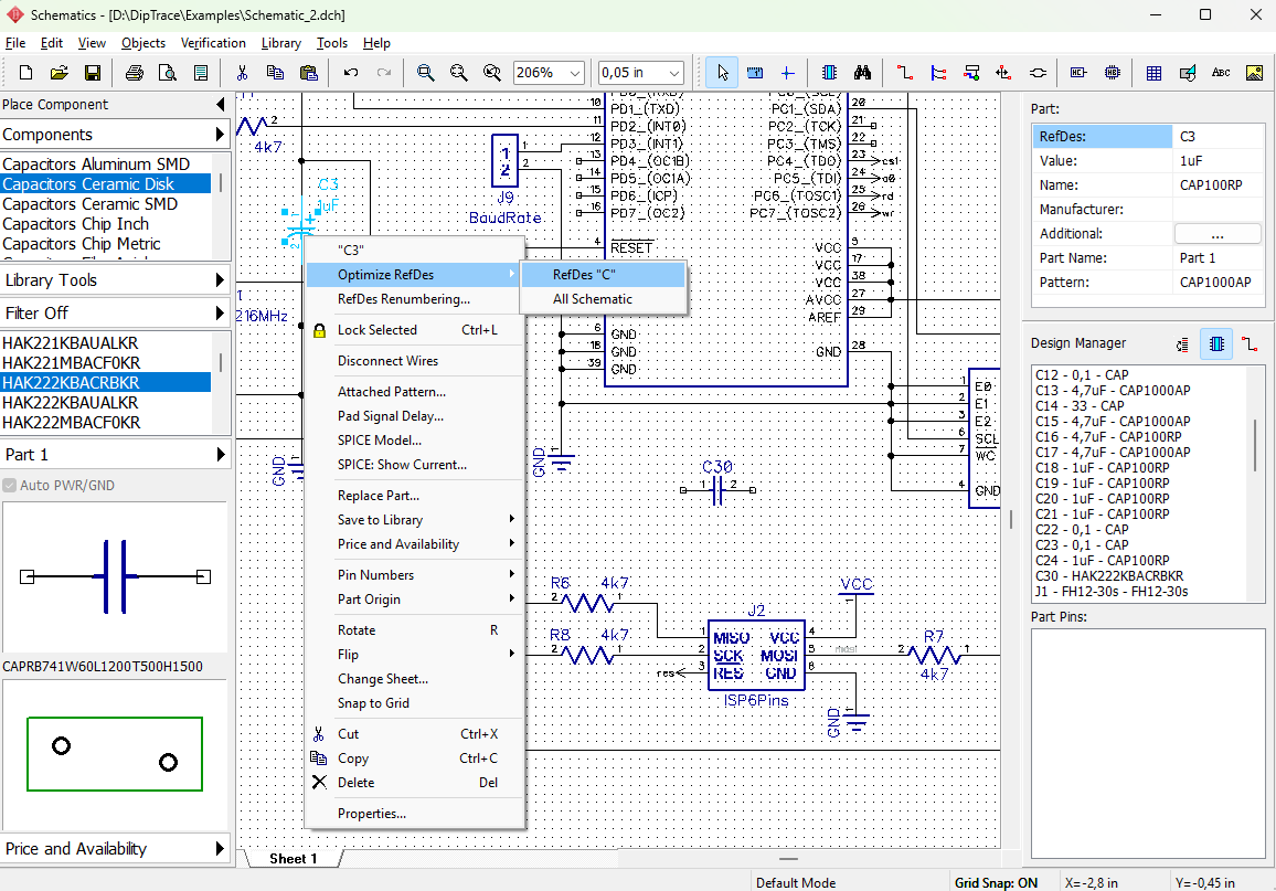
RefDes renumbering
What if we need to renumber Reference Designators in a very easy way that makes it simple to navigate through the schematic? Select "Tools / RefDes Renumbering..." from the main menu. In the pop-up dialog box do not change the First Index (starting point of renumbering) and Page Step (if page step = 100, the designators on the second page are R101, R102, IC101, etc.). Now specify the renumbering direction: in rows or columns, and choose how DipTrace is going to count components while renumbering. There are components of different sizes and shapes. If we choose Top-left in the Component Position section of the dialog box, DipTrace renumbers components, based on the position of the top-left corner of each component. If you choose Origin, the software considers component's origin to determine its position.
Notice that renumbering always goes from left to right and from top to bottom of the circuit.
Press OK to renumber all components.
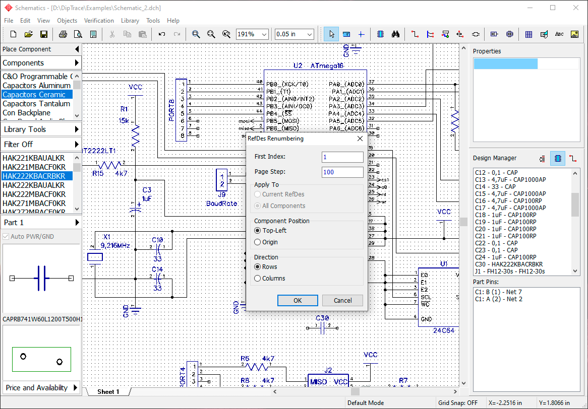
If you need to renumber only the designators of components of selected type, right-click on one of the components, and select RefDes Renumbering from the submenu. You see a typical RefDes Renumbering dialog box, but this time you can apply renumbering to the current RefDes.
RefDes Renumbering works the same in the PCB Layout.
Close DipTrace Schematic without saving progress and launch the PCB Layout module.
59. Placement and autorouting
DipTrace has advanced placement features and integrated auto-placer. This makes placement and layout optimization much easier.
Launch the PCB Layout module, select "File/ Open", and select "C:\Users\<UserName>\Documents\DipTrace\Examples\Schematic_4.dch" and use the schematic rules for this layout. You get something like in the picture below. The layout is chaotic because components are placed just like their symbols in the schematic. Manually arranging components would be a waste of time, this is why we recommend using the automatic arrangement, but, first, let's place a board outline.
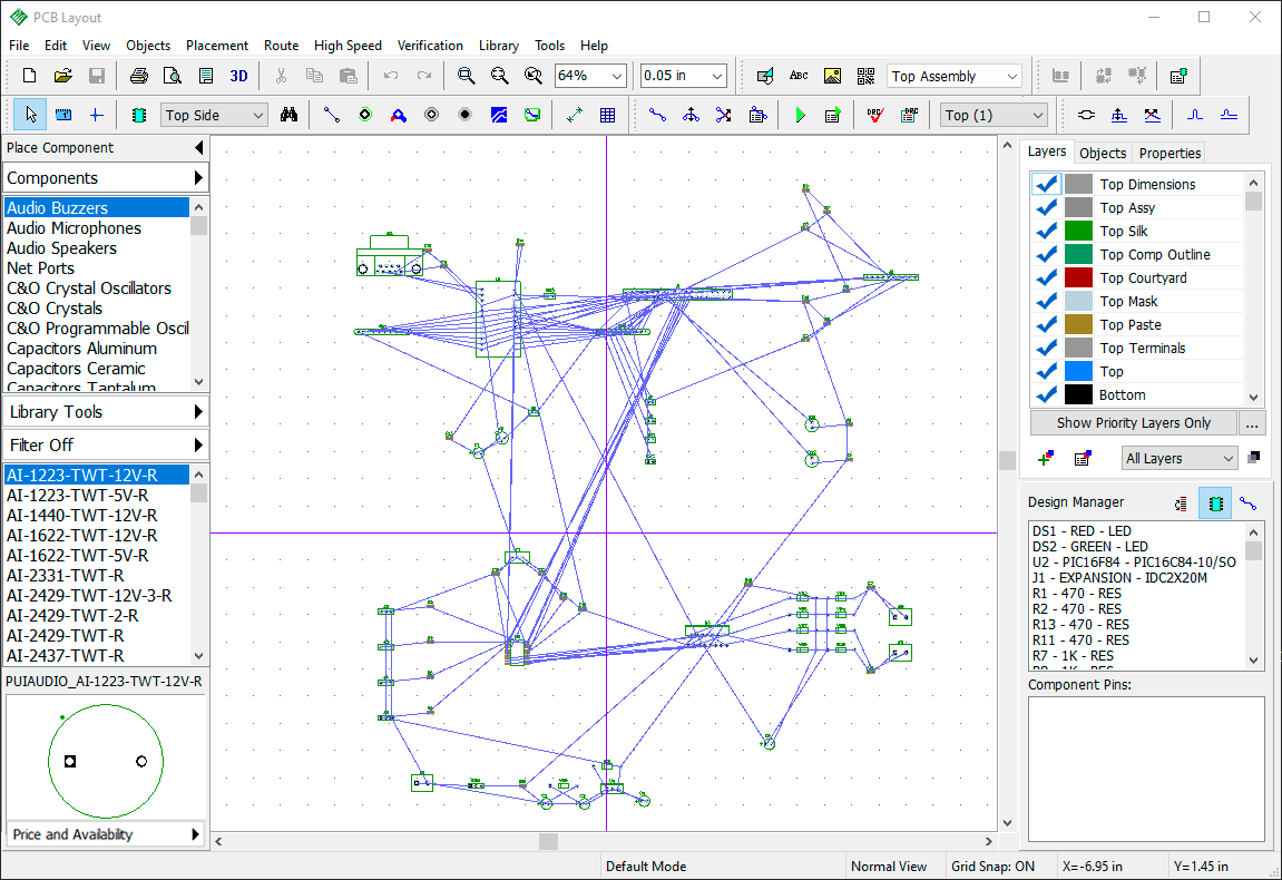
DXF import
We'll now import a board outline from a DXF file. Select "File/ Import / DXF" from the main menu and open "C:\Users\<UserName>\Documents\DipTrace\Examples\outline.dxf" file. In the pop-up dialog box, you can see a DXF file that will become the board outline. Select Board Outline DXF layer, and specify Convert to: Board Outline in a drop-down list below.
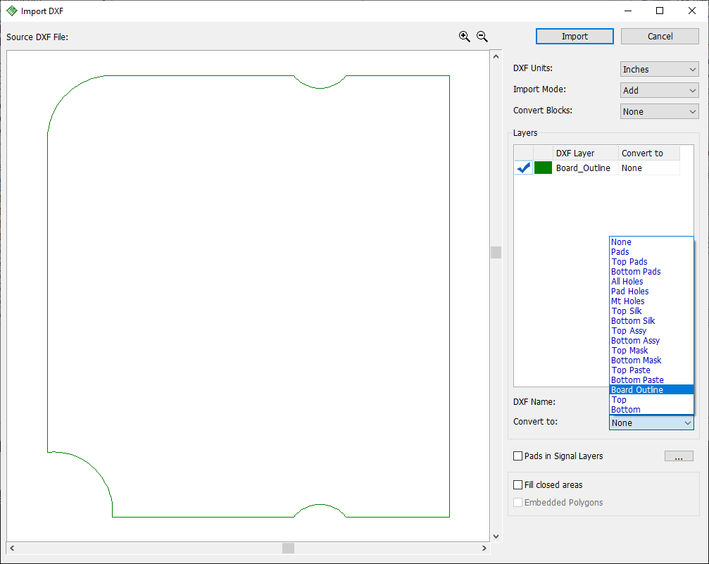
|
When importing component drawings or an entire layout from the DXF format, you can Fill closed areas and cut holes using Embedded polygons (usually DXF designs are made from the outlines without fills). This feature works for copper and mask/paste layers only. If you are importing pads in signal layer, then you can check the Pads in Signal Layers checkbox, and press
Select Import mode: Add to add board outline to existing layout, make sure inches are selected, and press Import button in the upper-right corner. The board outline appears on the design area, but components are still messed. Select "Placement/ Placement Setup" from the main menu: |
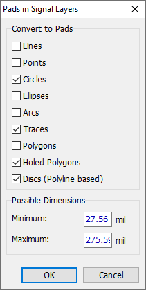
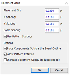
Check Place Components Outside the Board Outline checkbox to arrange components near the board outline. Keep other settings like in the picture above. Click OK to apply changes and press button on the Placement toolbar or select "Placement/ Arrange Components" from the main menu.
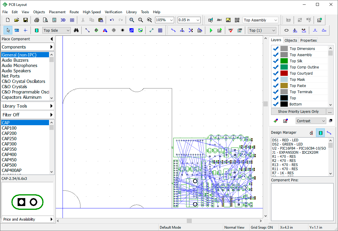
All components are now located in one place near the board outline.
Notice that Arrange components feature is not the same as Auto-placement.
Automatic placement creates a layout with a minimum possible total length of connections between the pads of components. Arrange Components feature simply brings all components to one place and makes it easier to work with them.
However, in real life manual placement is widely used, because most of the time we have certain places for certain components. DipTrace allows the user to combine automatic and manual placement on a single circuit board.
Placement by list
Select "Placement / Placement by List" from the main menu, then in the pop-up dialog box select component from the list (left-click it), move the mouse to the board outline, and click inside the board outline to place the selected component there.
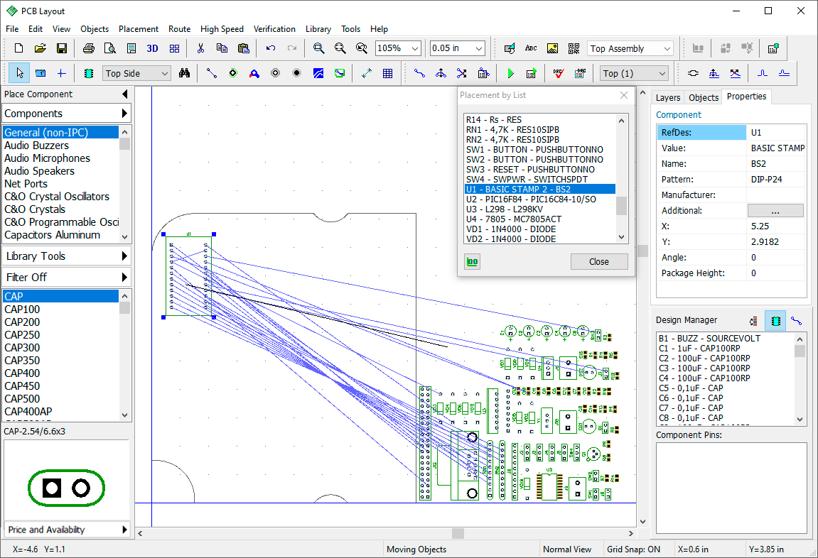
Component disappears from the list after placement (the list shows only those components that are outside the board outline). Position U1, U2, U3, J1, J8 and J12 components manually, like in the picture below. You can optimize connection lines with F12 hotkey or uncheck the Ratlines item on the Objects tab on the Design Manager to hide the ratlines. Close the Placement by List dialog box when done.
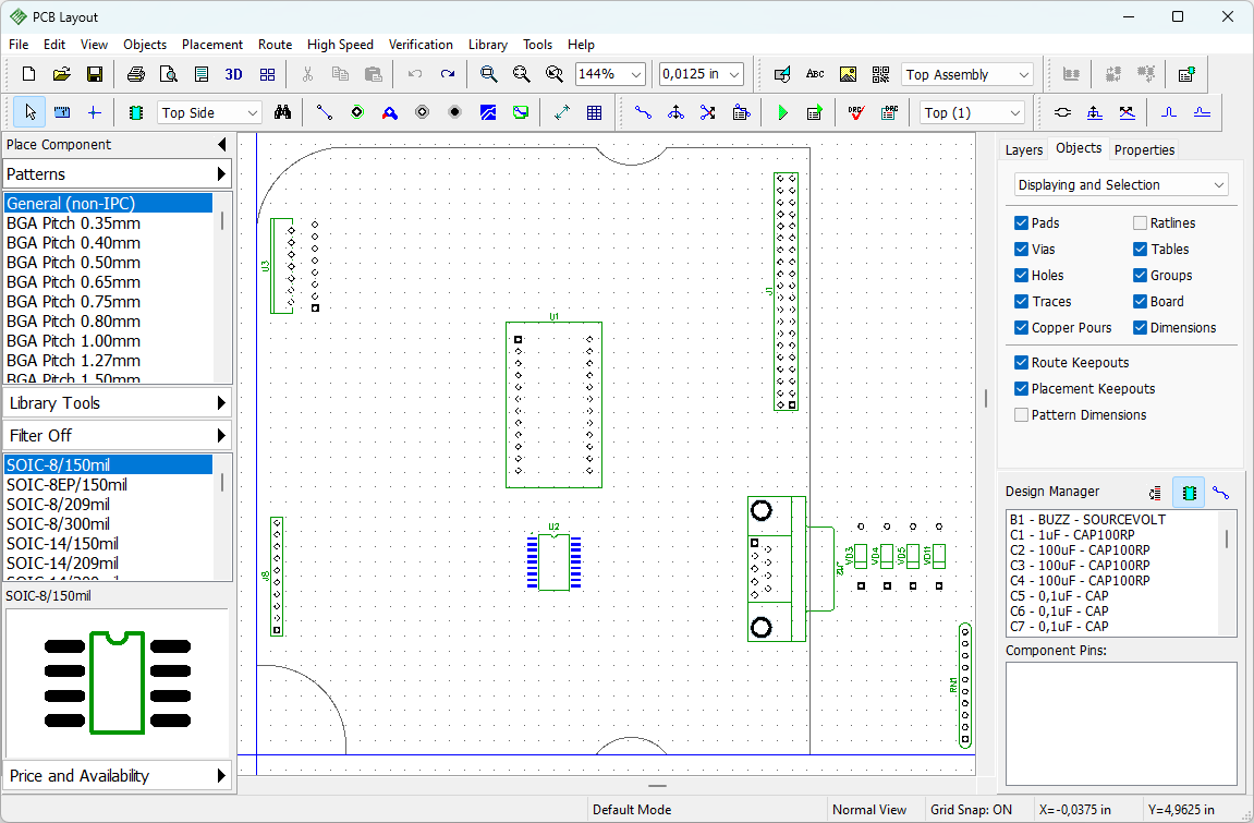
Place selected by list
Another way to place components in an organized manner is the "Place Selected by List" function. This tool allows you to select components in the related schematic and automatically get them organized into a list for placement in the PCB Layout module.
First, we are going to make sure that the Cross Selection is enabled. Navigate to Edit/ Cross Selection, and in the pop-up dialog, mark Enabled. The related schematic should already be correctly set since we started this project from an existing schematic file.
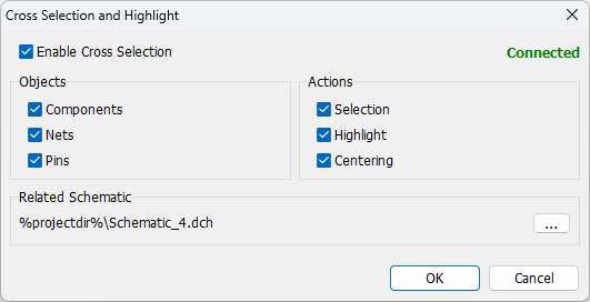
Next, launch Schematic Capture and open the Schematic_4.dch project from C:\Users<UserName>\Documents\DipTrace\Examples\Schematic_4.dch. Select components RN1 and RN2 in the schematic — these will automatically be selected in the PCB Layout.
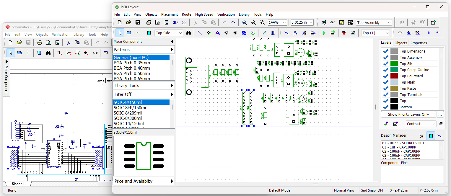
Now, go to Placement/ Place Selected by List, which will bring up a window listing the selected elements, ready for placement.
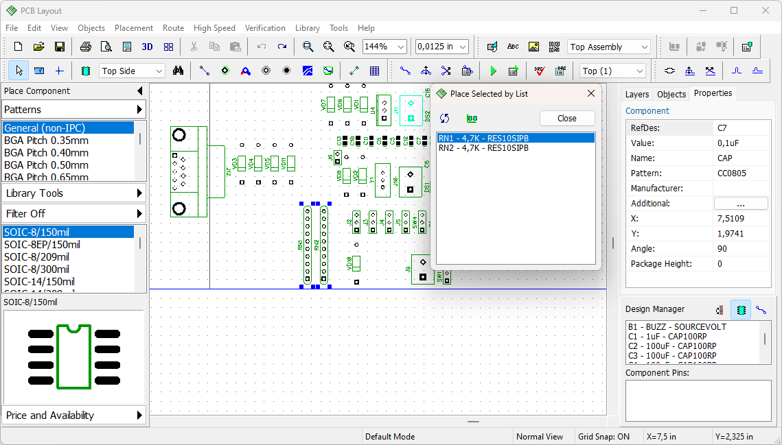
Simply drag the components from the list onto the board to place them. Once done, you can select another batch of components in the schematic, press the update button to refresh the list, and continue placing additional components. For this tutorial, however, we'll place just these two components using this function, as shown in the picture below.
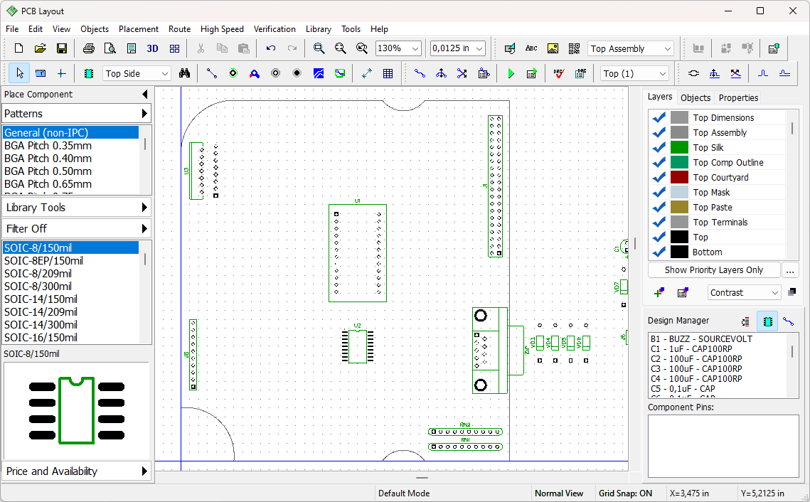
Custom component clearance
Default component clearance is set with X and Y spacings in the Placement Setup dialog box. We need all other components to be at least 20 mm away from the U3 component. Therefore, we will set a custom clearance for this component. Right-click on the U3, and select Properties from the submenu, then open the Other tab, and define: Use: Custom and Value: 0.79 inches (approx. 20 mm). Click OK to close the dialog box and apply custom clearance.
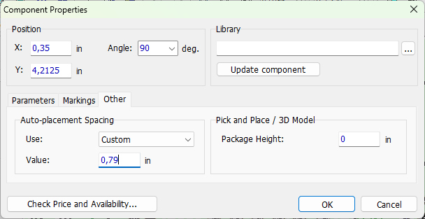
Now select all components which are already on the circuit board, and lock them (Ctrl+L hotkeys).
Auto-placement
We do not have special requirements for other components. Therefore, we can place them automatically with 5 mm spacings. Change measurement units (Shift+U keyboard shortcut). Select "Placement / Placement Setup" from the main menu, change X Spacing and Y Spacing to 5 mm, and set 3 mm board spacing. Make sure that Allow Pattern Rotation checkbox is checked (sometimes it is better to turn it OFF, for example, for single-sided boards with jumper wires). Uncheck Place Components Outside the Board Outline and make sure Use Pattern Spacings item is checked, this allows the program to use 20 mm (0.79 in) custom clearance of the U3 component. We do not recommend to check Increase Placement Quality option now (you can try it later).
Press OK to apply changes, and then press  button on the Placement toolbar or select "Placement / Run Auto-placement" from the main menu. DipTrace looks for the best location for each component. You will get something like in the picture below (notice that Design Manager panel is hidden (Ctrl+2 hotkeys), the ratlines are also hidden).
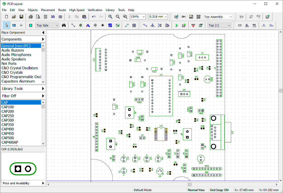
Some connections are not optimal because we have placed large components manually. If you auto-place the entire board, you can get better results, but usually, this is not the option in real life.
It's clearly visible that there is no component on the board closer than 20 mm to the U3 because of the custom clearance.
Autorouting with net classes
Check via properties in the "Route / Via Styles" main menu item. One via style is enough for this project (we'll use 1.2 mm via with 0.6 mm hole). Now we need to create a separate net class for Power and Ground nets because traces of these nets should be a bit wider. Select "Route / Net Classes" from the main menu. All nets belong to the Default class. Press Add button to create a new net class, then select it from the list, and enter its name ("POWER"). Specify: Trace Width: 0.6 mm, Clearance: 0.6 mm. Press Clearance Details button and in the pop-up dialog box set Trace to Pad: 0.5 mm. Now press OK. Select VCC and GND nets from the list of all nets of the project in the lower-right corner of the dialog box (use Ctrl key for multiple selection) and add them to the POWER net class (press button above the list).
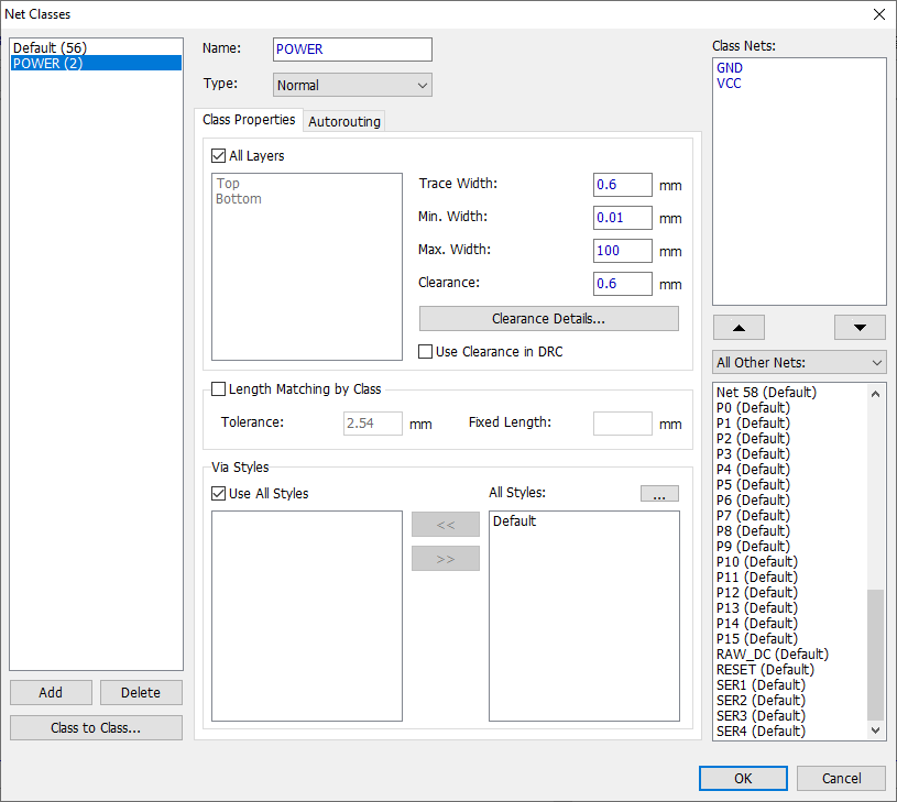
Now select Default net class, and specify the following parameters: Trace Width: 0.4 mm, Clearance: 0.4 mm, Trace to Pad: 0.3 mm. Use all via styles for both net classes (as you remember, we have only one via style). Press OK to close the Net Classes dialog box. Make sure that Shape Router is active ("Router / Current Autorouter / Shape Router"), then go to the Autorouter Setup dialog box, and in the Settings tab uncheck Use Priority Layer Directions.
Now press Ctrl+F9 or the  on the Route toolbar to launch the autorouter. In a few seconds you will get the results. Change layer colors if you want.
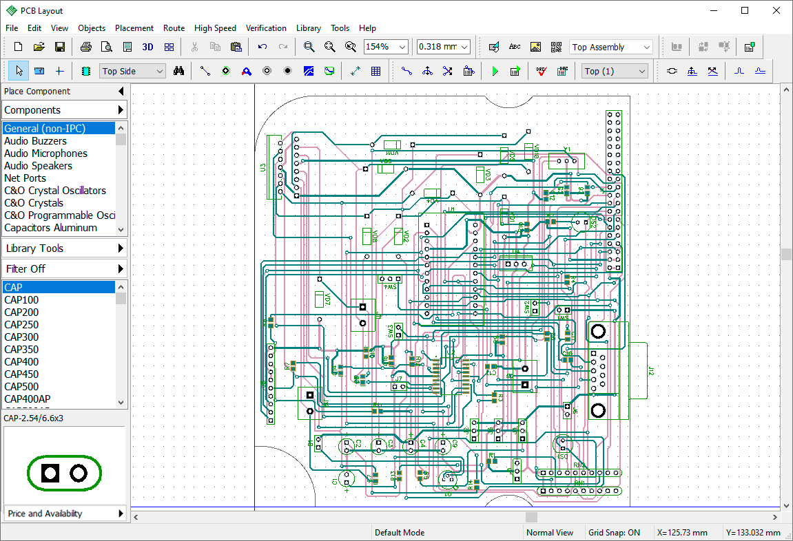
A detailed description of the autorouter settings is available in the PCB Layout Help ("Help / PCB Layout Help" from the main menu). If you still have some unrouted nets, Undo, change trace width/clearance, placement or other settings, then launch autorouter again. However, if you have followed the beforementioned instructions you should not get any problems.
60. Layer stack
DipTrace allows for comprehensive control over the stack of conducting and insulating PCB layers in the Layer Stackup dialog box and generates a stack table that clearly documents the PCB stack for manufacturing engineers.
Launch DipTrace PCB Layout module and open the PCB_6.dip file from the "Documents/DipTrace/Examples" folder. It is a 4-layer circuit board. Select "Route / Layer Setup" from the main menu or press  button on the Layers tab, then press the Layer Stackup button in the Layers dialog box.
In the Layer Stackup dialog box, you can see the table which represents a printed circuit board's cross-section. In our case, DipTrace has automatically selected the 4 Layers Default Stackup in the Template drop-down list because this design has two signal layers and two plane layers.
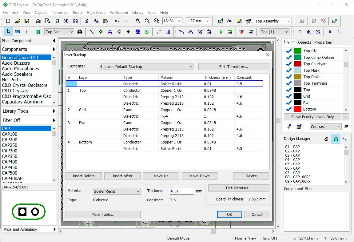
There are many variations of PCB stacks on the market, but default stackups available in the software are usually the most common and thus the cheapest ones. However, you can create any stack. As you can see from the list, this 4-layer stackup is based on a single FR-4 core and additional prepregs to separate copper layers. For this tutorial, we will create a 4-layer stack based on two FR-4 core layers and capable of conducting large currents (like in the picture below). This stackup is a bit rare because of certain hole-plating difficulties, but it is a good example.
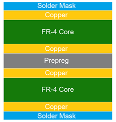
First of all, let's change the copper thickness to 2 Oz to conduct large currents. Usually, it is the thickest copper that does not skyrocket the manufacturing price and is available at most PCB houses in stock. Left-click on the layer #1 Top in the list, and select Copper 2Oz material from the Material drop-down list, then do the same for all conducting layers. Because the copper layers become thicker, the overall board thickness of the circuit board is recalculated automatically.
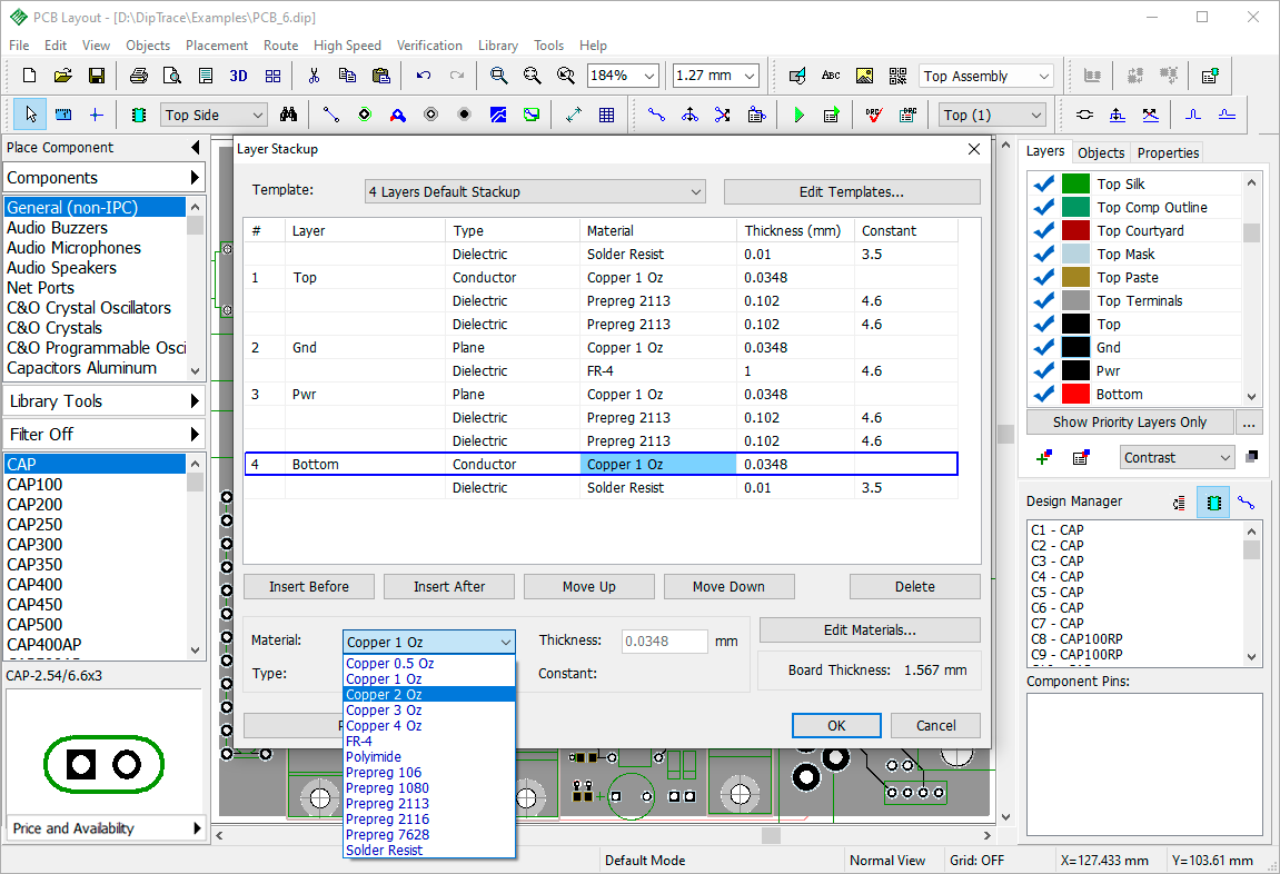
Notice that you can use Shift + U hotkeys to change the measurement units on the go. All values are instantly recalculated.
Now left-click on the Prepreg layer right below the layer #1 Top, and change its material to FR-4 substrate, then select another dielectric Prepreg 2113 layer, and move it down the stack (press the Move Down button). Now left-click on the FR-4 layer below the layer #2 Gnd, and move it down. The final steps are deleting one of the prepregs left, and moving the other prepreg up the list because we want to have double-layered 2113 prepregs separating the copper layers (like in the picture).
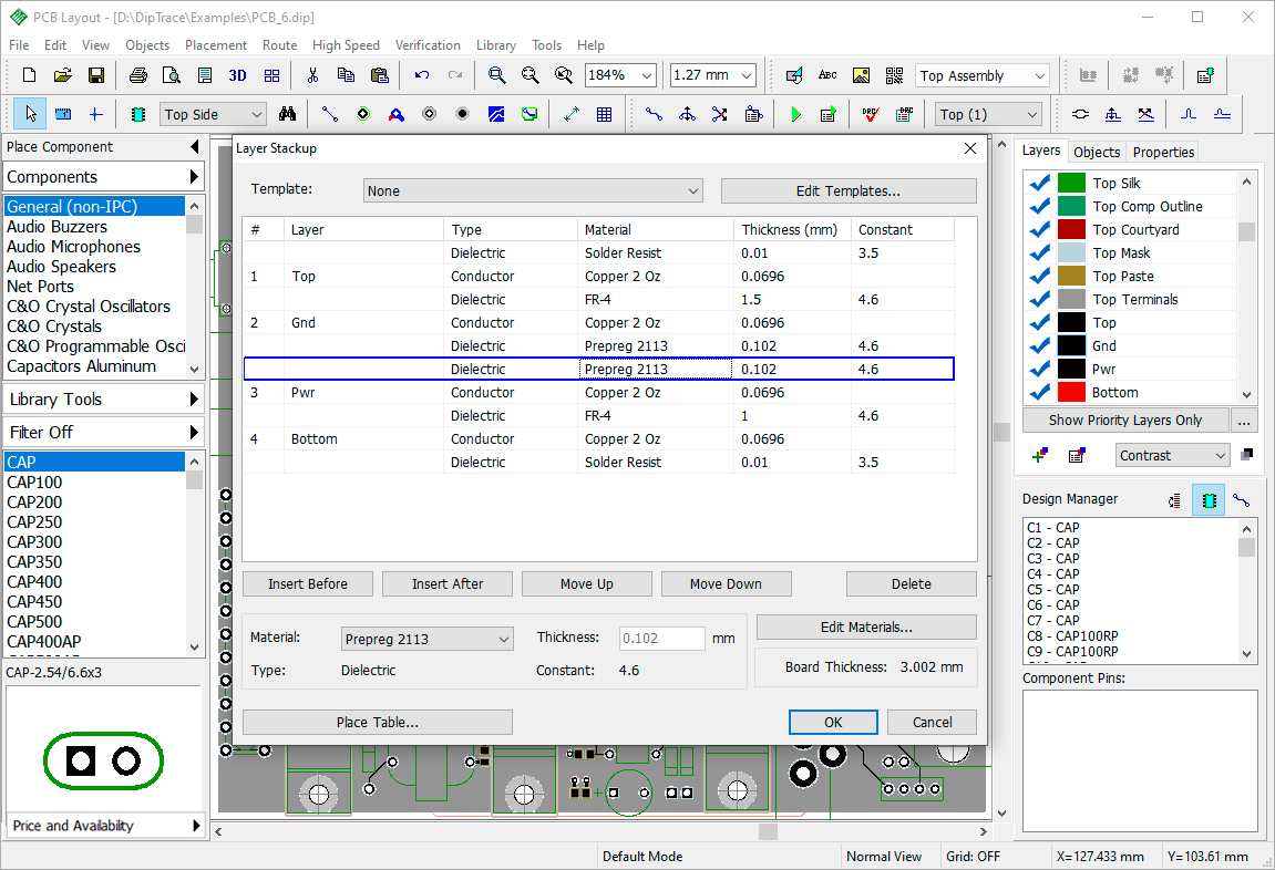
The final stage is documenting the layer stackup in the Gerber file for a PCB house. Press Place Table. In the pop-up dialog box, select a non-signal layer for placing the layer stackup table (Top Assembly layer is the best choice); you can change fonts, measurement units and preview the total dimensions of the Layer Stackup table.
Press Place, and left-click on the design area to place a Layer Stackup table on that spot. The thickness of the layers in the stack influences the via height and is taken into account by phase tune and trace length measuring tools. Hence, the software can ask if you want to consider the stackup of layers for trace length calculation (if it is not considered yet).
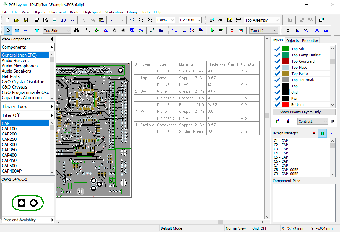
Notice that the table is automatically updated. You can use Shift + U hotkeys to change measurement units on the go. All values are instantly recalculated.
The color of the table depends on the color of the PCB layer. Now the manufacturing engineer can understand which layer stackup you prefer. However, it is better to consult your PCB house before making changes to the layer stack.
Don't save any changes in the PCB_6.dip file.
Add new materials to the stackup
|
If you can not find the material you need in the list of available materials in the Layer Stackup dialog box, press the Edit Materials button. The Layer Materials dialog box pops up, here you can add new and change properties of existing materials (Type, Thickness, and Dielectric Constant). All materials are divided into three basic types: Conductor, Plane, and Dielectric. Use the corresponding buttons to add/delete /edit materials. |
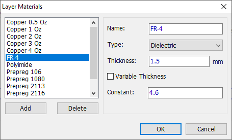
Check Variable Thickness box to allow for changing the layer thickness directly in the Layer Stackup dialog box.
High-speed nets and differential signals
Length matching and signal timing
61. Length matching
One of the core challenges with routing high-speed nets is controlling that certain critical signals arrive at correct time. To achieve signal synchronization, the copper tracks needs to be roughly the same length.
DipTrace has an elegant solution for matching trace lengths that helps when routing high-speed data buses or any critical signals that require precise timing.
We will use one of the standard DipTrace PCB examples for practice. Launch DipTrace PCB layout, and open the "BGA_Autorouter.dip" file from the "Documents/DipTrace/Examples" folder.
If you're routing a high-speed bus, we recommend creating a separate net class for the bus. This will automatically create a DRC length matching rule. However, you can also select several nets and generate the length matching rule for the DRC without creating a net class.
Length matching a bus
First of all, we need to create a separate net class that hosts all the nets that we need to length match (Net 306 - Net 310). In this case, we have the "Memory" net class with several nets connecting the U6 FPGA with the U14 memory module. When all traces are added to the net class, check the Length Matching by Class check box to create a new length matching rule verified by the DRC.
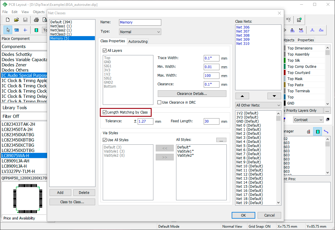
You can compare traces against the Fixed Length parameter or against each other with required Tolerance. Don't change the default tolerance value and let's say we need approximately 30-mm traces. Enter "30" in the Fixed Length field (the tolerance value automatically changes to 1.27 mm, which means a range of 2.57 mm over and under the fixed length). Press OK to create the net class and the rule.
Select "High Speed / Length Matching" from the main menu or right-click on the track, and select Length Matching, then Open Length Matching from the submenu. In the pop-up dialog box, select Memory (actual name of the net class) in the Rule drop-down list. All nets of the memory data bus, which we assigned to the Memory net class, appear right below. Some of the nets are highlighted in red to show the length tolerance violation. Left-click a net in the list to show it on the design area or hover over a net to highlight it. In our case, there are four nets that should be edited to comply with the rule.
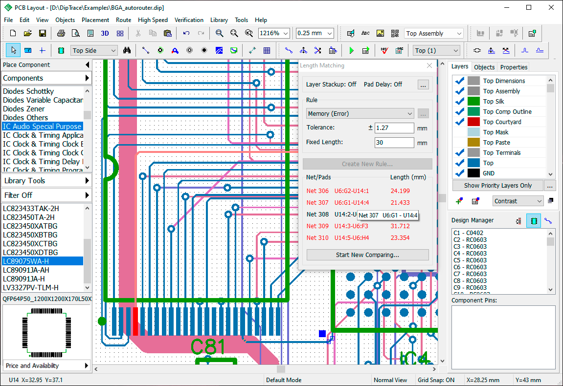
The most efficient way to make traces longer is drawing meanders.
Add Meanders
Select "High Speed / Add Meander" from the main menu or press  on the High Speed toolbar. Now hover over the trace, and drag and drop to draw a meander. Meanders are created one at a time. Move the mouse cursor to the right and create more meanders. The software helps to create meanders of the same size. Drag and drop meanders' lower vertices while holding the left mouse button to get something like in the picture below.
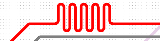
You can notice that the length of the trace is recalculated in real time. Once the trace length is around 30 mm ± 1.27 mm, the net is not highlighted in red anymore.
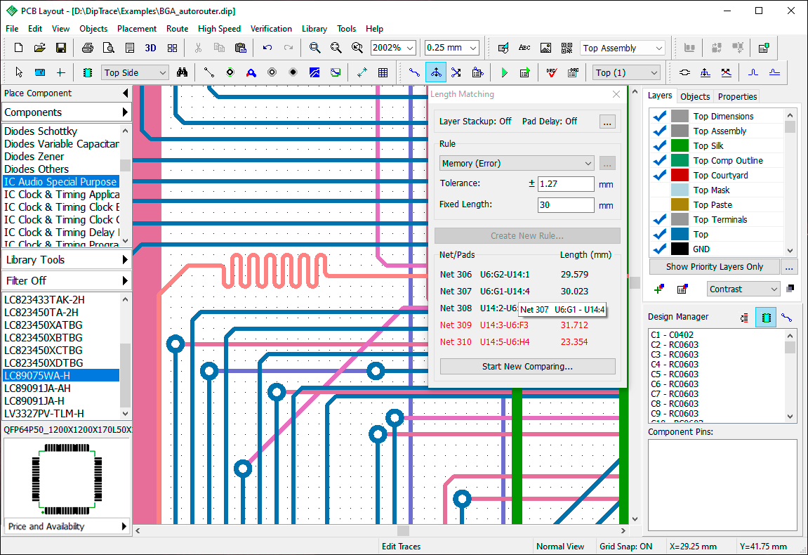
DipTrace can consider via height (derived from the layer stackup) and pad signal delay when calculating the trace length. Press the corresponding button in the Length Matching dialog box, and check Enable Layer Stackup and Enable Pad Delay check boxes. Since there are traces crossing between layers, some of them might fall outside the length matching tolerance and will require more or bigger meanders.
Edit Meanders
To push meanders along the trace segment, press the button (if not in the Add Meander mode already), left-click on the trace segment opposite the preferred direction, and drag and drop meanders.

Notice that you can also move meanders along the traces and change meander's amplitude in the regular Edit Traces mode ( button).
By default, the gap between each meander is defined by the net class clearance. To set custom meander gap, right-click on the trace, and select Meander Gap from the submenu. In the pop-up dialog box, check Value, enter a new gap (for example 0.3 mm), and press OK.
Notice that it's better to avoid any sharp angles when routing traces of high-speed nets.
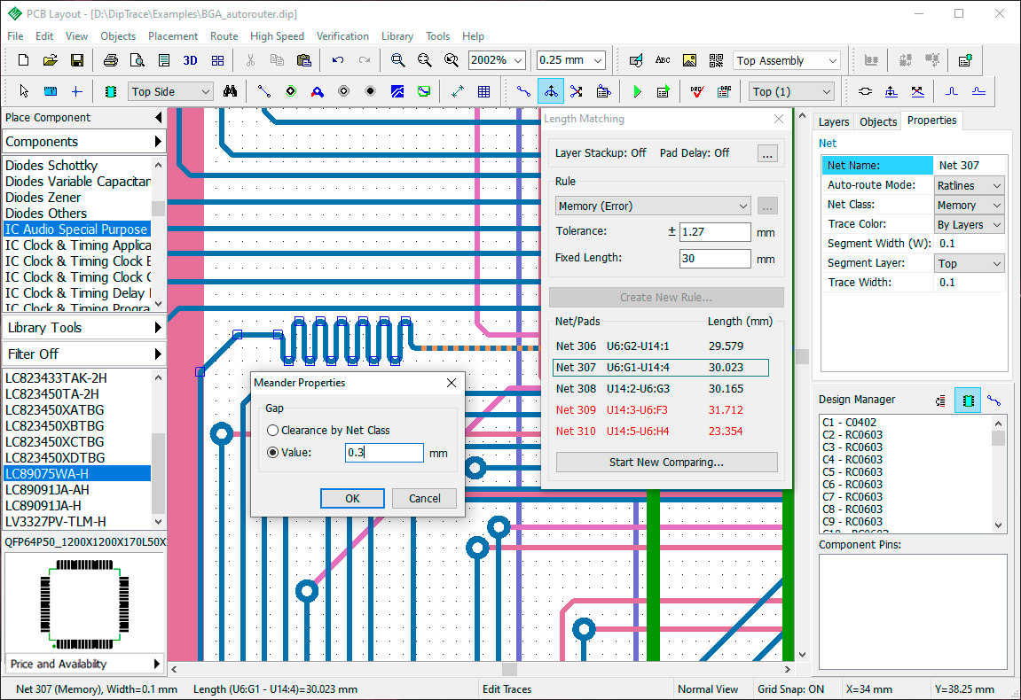
Fix all other errors by adding meanders and editing other traces.
Length matching nets
You don't have to create a new net class to length match some nets, just right-click on a trace segment or net in the list of nets on the Design Manager panel, and select "Length Matching / Add Selected Nets" to launch the Length Matching dialog box. You can also select several segments of different nets, and select "Length Matching / Compare Selected Nets Only" from the net submenu. In the Length Matching dialog box, you can compare nets against each other or against a fixed length.
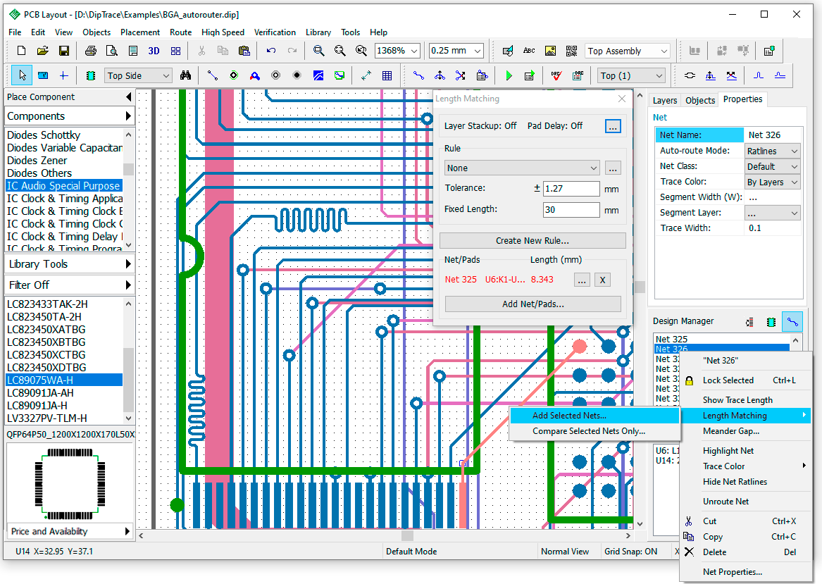
You have to create a new rule (press Create New Rule, and enter a name in the pop-up dialog); otherwise, the DRC does not verify the length matching constraints.
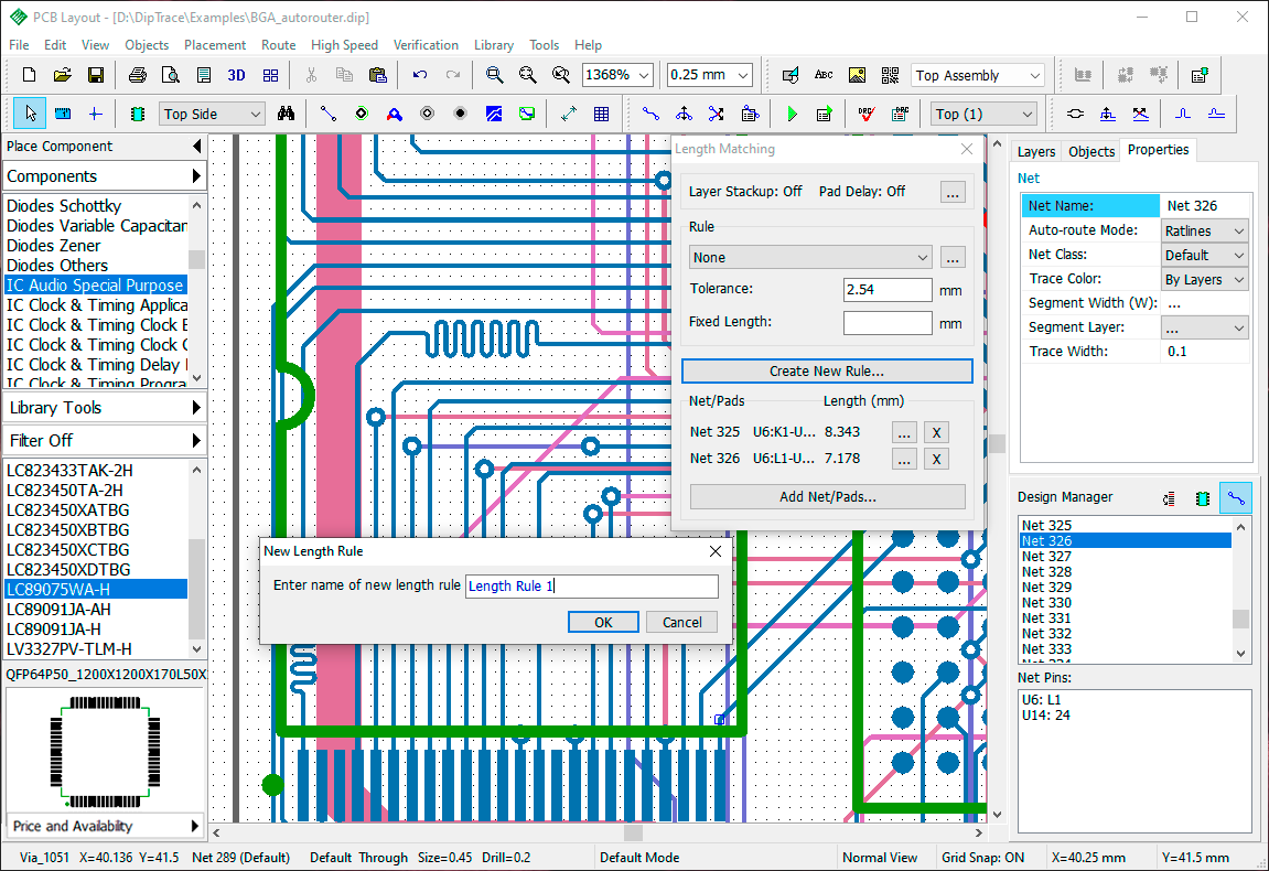
Press OK to create a rule.
You can also add new nets to the comparison with Add Net/Pads button.
If you work with nets that have more than two pads and you want to length match only certain track of the net (trace between two pads), select the corresponding pads from the drop-downs after selecting the net in the Add Nets/ Pads dialog-box.
62. Signal delay
Bond wires are the wires inside electronic component's package that connect pads to the die. These wires introduce a signal delay, which should be accounted for in high-speed designs. Manufacturers report this in-device pad signal delay in the datasheets in picosecond time or as a length.
Pad signal delay value is considered for phase tuning and trace length matching and is added to the total length of the traces. We recommend setting up signal delays when designing a component in DipTrace Component Editor, but you can also set delays in the Schematic and directly in the PCB Layout.
To set pad signal delay in the PCB Layout, right-click on the component and select Pad Signal Delay from the submenu or right-click on the pad and select Signal Delay. Select the pad from the list (if not selected already), and enter a signal delay in mm, mils, or inches right below (use Shift + U hotkeys to change the measurement units on the go).
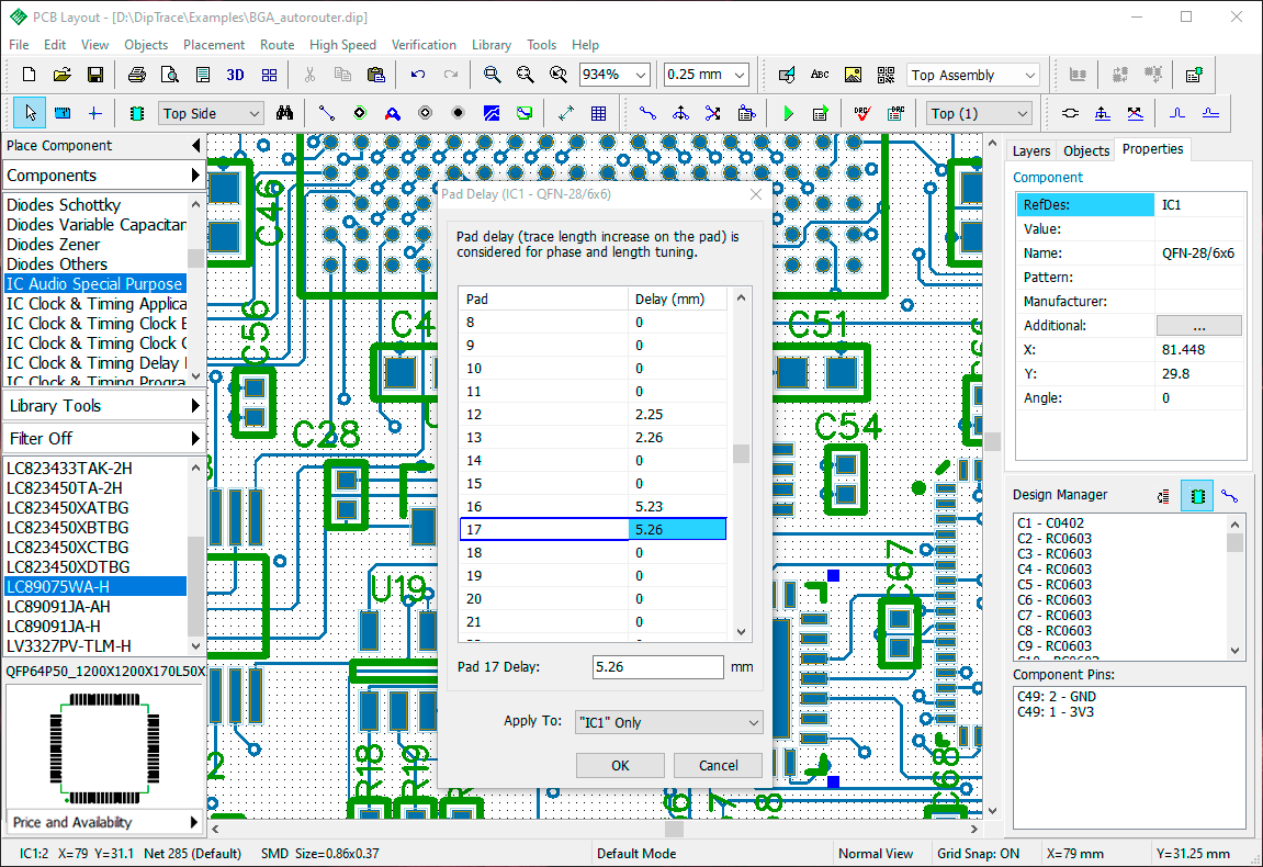
Select if you want to apply signal delay parameter only to the selected component or to all components with the same name on the circuit board. Press OK to apply changes. If DipTrace is not using Pad Signal Delay value for trace length and phase calculation, it drops a warning message that suggests you apply pad signal delay values to trace length calculation, press Yes in the Warning dialog box.
You can turn ON/OFF the considering of pad signal delay for trace length calculation, just go to "High Speed / Length Matching" from the main menu, press button at the top of the pop-up Length Matching dialog box and check/uncheck Enable Pad Delay item.
Differential pairs
63. Create a differential pair
Differential pair signaling is a method of transmitting high-frequency signals using two tightly coupled tracks on the circuit board. One track carries the signal and the other one carries an equal but opposite image of the same signal. Differential pairs are EMI immune, they generate less noise than single-track connections and, basically, are the only acceptable way of transmitting information at high speed.
Open DipTrace Schematic, and go to "Objects / Net Classes" from the main menu. In DipTrace, all differential pair parameters are governed by net classes, and the program does not allow the user to create differential pairs outside of them. We need to create a new special-type net class for differential pairs. Press Add button in the Net Classes dialog box, then type in the name of the net class (for example, "Diff_Class_1"), and change Type to Differential Pair. Now you can enter specific differential pair routing parameters.
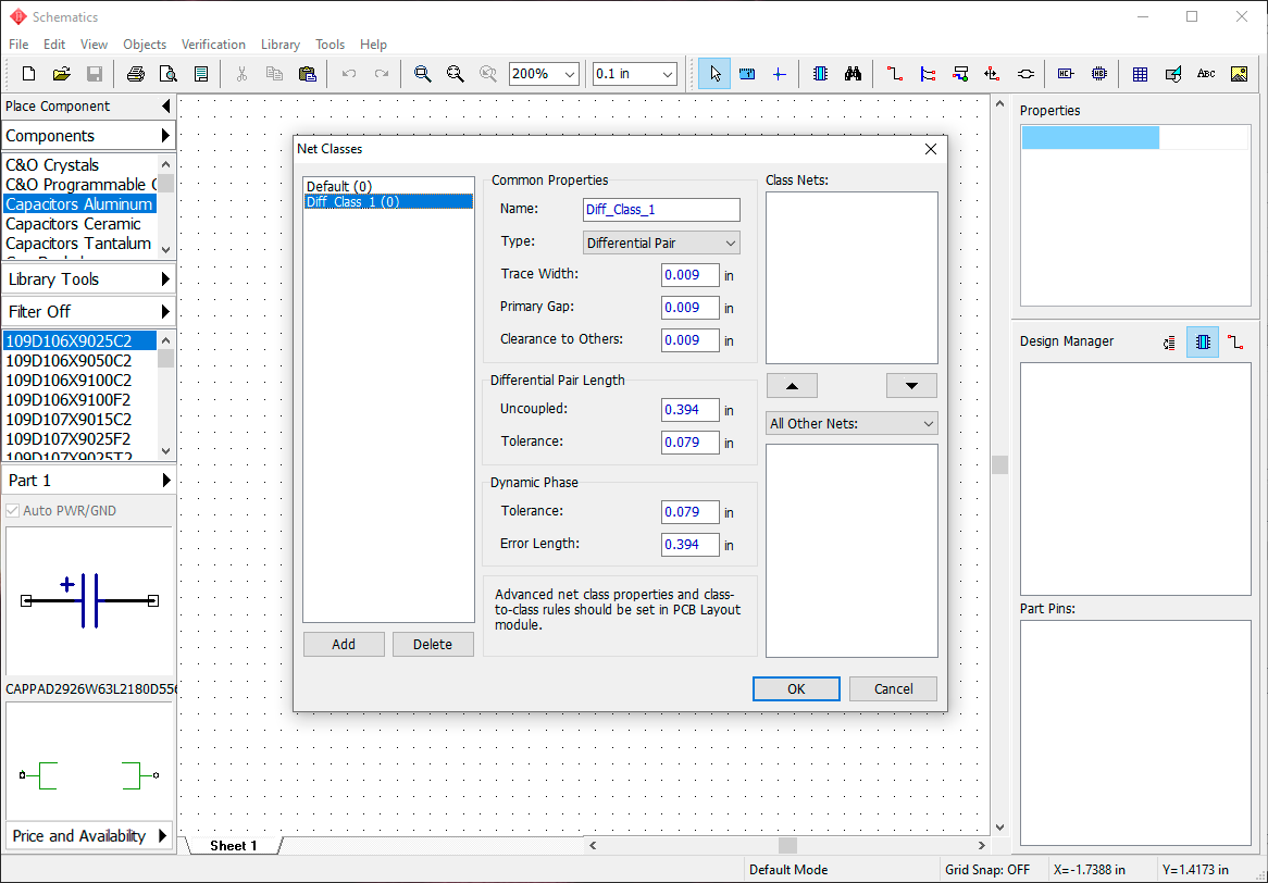
Enter the trace width for tracks of the pair, the primary gap between the tracks, and clearance to other objects on the PCB (for example, 0.009 inch, like in the picture above). You can leave default values in other fields. Notice that the net class is empty (because the design is empty itself).
Press OK to close the Net Classes dialog box and apply changes.
Now we need to populate our schematic with components for practicing with differential pairs. We have ATSAM4LC8BA-UUR (IC MCU Atmel ARM library) flash memory module and EPM7128AETC100-7 (IC Embedded CPLD library) chip on the design area, but differential pair declaration can be assigned to any nets between any components. So, you can use any components of your choice. Create two nets which will eventually become a differential pair. For example, we have Net 0 connecting the D1 pin of the flash memory to pin#13 of the CPLD-component and Net 1 – connecting C3 to pin#14.
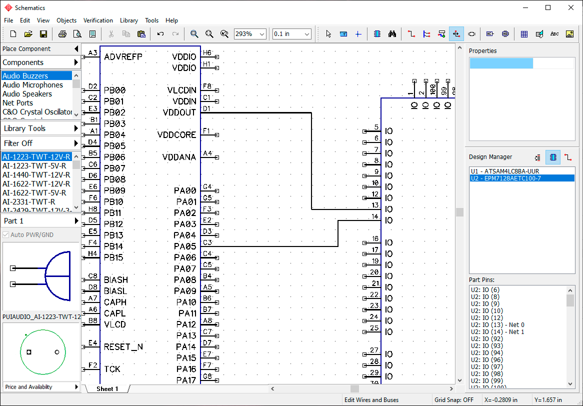
Now press  button or select "Objects / High Speed / Define Differential Pair" from the main menu. In the pop-up dialog box, specify the positive and negative net of the differential pair. For example, we select Net 0 in the Positive Net drop-down and Net 1 in the Negative Net drop-down. You can also pinpoint nets directly on the design area by pressing
  or
or  buttons and left clicking on the nets or their pins.
Since we have only one differential pair net class, the program automatically assigned Diff_Class_1 to this differential pair. Net class properties are right below. Press Edit Net Classes if you want to open the Net Classes dialog box and change differential pair properties.
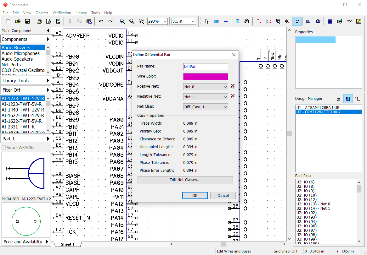
Press OK. Net 0 and Net 1 are a differential pair, these nets are renamed to DiffPair_P and DiffPair_N respectively and marked with special symbols on the design area. You can hover over one net with the mouse and the other net of the pair highlights. You can display net names on the design area if you right-click on each net, and select Display Name from the submenu.
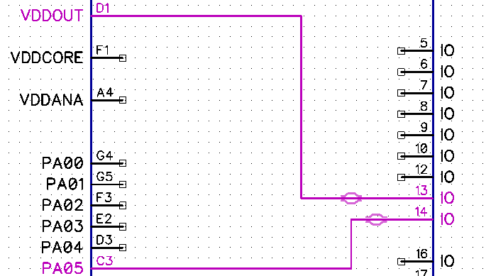
Now let's switch this design to the PCB Layout stage and practice more in customizing, routing, and verifying differential pairs. Proceed to the next topic of the tutorial.
64. Differential pair routing/editing
Notice that built-in DipTrace autorouter does not support differential pairs. We recommend routing these nets manually or with external autorouters.
Select "File / Convert to PCB" from the main menu in the DipTrace Schematic, and proceed with the schematic rules. In the PCB Layout, move components closer together. You can see that differential pair is also marked with a special symbol, like in the schematic. You can see that ratlines are twisted, it's possible to route the differential pair like that, but it would be much easier to rotate the U2 pattern to eliminate the twist. Select the component, and press R hotkey two times to rotate the component 180 degrees. Now we're almost ready to start the routing, but, first, we need to go to the Net Classes dialog box to check if we have acceptable routing parameters. Select "Route / Net Classes" from the main menu, then select Diff_Class_1 net class.
Differential pair routing parameters. DipTrace allows the user to specify various differential pair routing parameters. DRC takes these values as routing constraints when verifying the PCB. You can specify the maximum uncoupled length for two traces of the differential pair, length tolerance between the traces, dynamic phase tolerance (length difference between corresponding segments of each track), and phase error length which means that DRC will report any phase shift as an error only if it occurs on the track segment longer than the Error Length value. Let's change the Dynamic Phase Tolerance to 0.04 and Dynamic Phase Error Length to 0.3 inch. Leave default values in other fields.
Since we have some small-pitch BGA footprints on the board, we can estimate that our differential pair with 0.009 inch wide tracks, gap and clearance is too big to be routed. DipTrace allows the user to define neck parameters which can be easily applied to differential pairs while routing in tight spaces. Press Neck Parameters button.
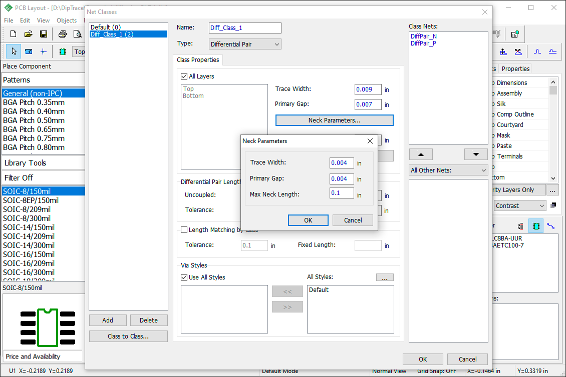
In the small pop-up dialog enter 0.004 inch width and gap, and 0.1 inch as the maximum neck length. This means that necked segment longer than 0.1 inch will be reported as an error by the DRC. Press OK to apply neck parameters, and then press OK to close the Net Classes dialog box.
Let's create one more differential pair directly in the PCB Layout. First, we need to create a couple more nets with Place Ratline tool  . For example, like in the picture below.
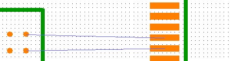
Then press Define Differential pair button ( on the High Speed toolbar). Define Differential Pair dialog box shows up (this dialog is the same as in the Schematic module), pinpoint the positive and negative nets, change color for convenience (red in our case,) and apply the same Diff_Class_1 net class to this differential pair. Press OK and the second differential pair with custom color appears on the design area.
Now press button on the Route toolbar, or go to "Route / Manual Routing / Add Trace" from the main menu, and left-click on any pad of the differential pair – two tracks starts to appear simultaneously. Routing a differential pair is very similar to routing a single net. Ratlines show the direction where to lead the traces. Continue from the U1 component to the U2, and left-click on the corresponding U2 component's pad. The second trace of the pair will be automatically connected to another pad. You can change the routing layer, route mode, current trace segment, and other routing parameters on the Routing panel, with the corresponding hotkeys (noted in the brackets on the Routing panel) or with the right-click submenu on the go.
If you want to change an active trace of the pair that you route, select Change Control Trace from the right-click submenu while routing.
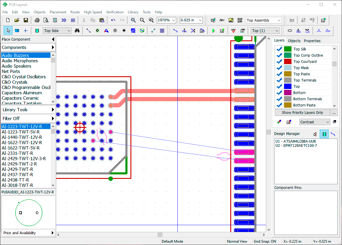
Single-track routing
In real life, you will often face more complex layout situations. Press button on the Route toolbar, or go to "Route /Manual Routing / Add Trace" from the main menu. On the Routing panel you can customize the set of the segments that will be used during routing. Select My Routing Mode and press button; in the menu tick 90 > 45, 45 > 90 and free line segments, press OK. Now click on the Current Segment image and select Free Line (press S hotkey two times). Start routing the first differential pair from U2 to U1. You will notice that BGA pitch is very small and now is the time to apply the trace necking defined earlier in the Net Class properties. When approaching the U1, left-click to place the trace segments, and then right-click, and select Neck-down Segment from the submenu to reduce the width of both tracks and the gap between the traces according to the neck parameters. Left-click again closer to the U1 component to create a small narrow segment (orange traces are routed). Now the tracks are small enough to fit the BGA's pitch, but you still can't finish routing the pair automatically. Hover over the terminal pad to see that the traces offered by the program are unacceptable.
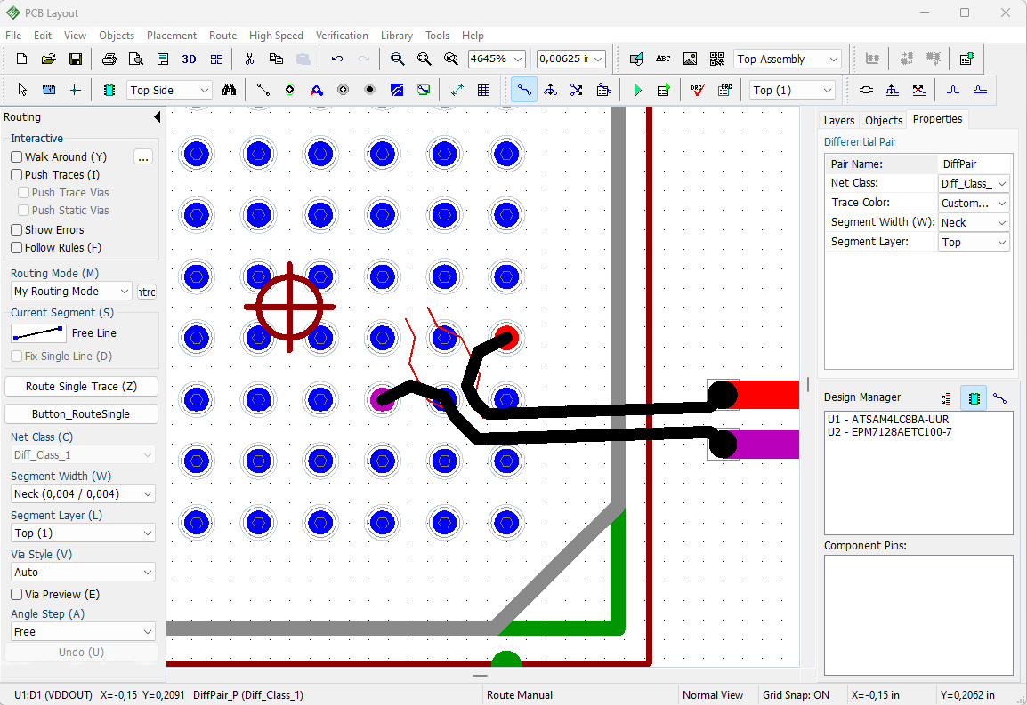
Routing each trace of the differential pair will allow you to succeed in this situation. Right-click, select Route Single Trace from the submenu or press Z hotkey, then change current segment to regular lines with a 45-degree angle on the Routing panel (or just press S hotkey), then left-click on the terminal pad of the trace. DipTrace will switch to the second trace of the pair for routing. Left-click on the second pad to complete the differential pair.
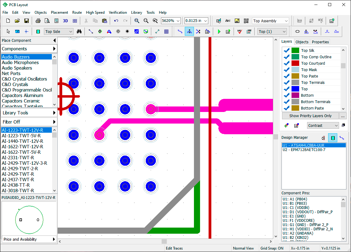
If you want to change the trace of the pair that you are routing, select Change Control Trace from the right-click submenu.
Controlling the trace length
Controlling the total length of each trace is very important for successful high-speed routing. Right-click on any trace of the differential pair, and select Show Trace Length from the submenu, the total length of each track of the differential pair will appear right next to the pads of the differential pair in the current measurement units. To hide the trace length, select the same item from the same right-click submenu again. In our case, the trace length is hidden to keep design more empty and easy-to-understand.
Edit differential pairs
Right-click on the differential pair, and select a required action from the submenu. You can unroute tracks or separate segments, change the color of the differential pair, the layer of the traces or segments, delete differential pair declaration from the nets, remove necking, and much more. There are two distinct editing modes applied to differential pairs: regular editing and single track editing. Each one can be in a regular or free style. For example, press button on the Route toolbar, then drag and drop differential pair's traces to another location. Notice that two tracks move respecting the differential pair gap. You can also use the Free edit tool ( button) in some situations.
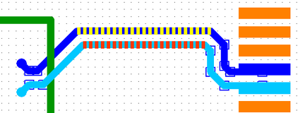
The other mode is similar to single-track routing because it allows the designer to edit each trace of the differential pair separately from the other. Press  button on the High Speed toolbar, and move one track of the pair further away.
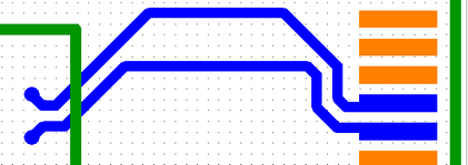
Single-track free edit mode (  button on the High Speed toolbar) behaves in a similar way to the regular Free edit mode, but applies only to one trace of the pair. You can practice more with differential pairs and change the layer of the trace segment. Right-click on the longest differential pair's segment, and select "Segment Layer / Bottom". Two traces will move to the bottom layer. Vias will appear automatically.
Please undo the last changes to return the red differential pair to its initial state.
65. Phase tuning a differential pair
We have Real-time DRC OFF, this is why we do not see any errors on the design area. Turn it ON, and launch the DRC in the regular mode to see the error-report dialog box. DRC checks all clearances and sizes against the target values defined in the "Verification / Design Rules" main menu item. DRC also takes differential pair properties from the Net Classes dialog box as design constraints. In our case, we have three errors related to the differential pair. When you click on the error in the list, you see the description of each violation, including the current and the target values. Rule Details section right below the list shows where the target values are defined.
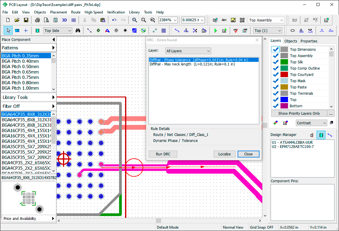
Move the DRC Error-report dialog box a bit, so that it does not obstruct the view over the design area, and start fixing the errors. First of all, let's make the necked differential pair segment a bit shorter, as we can see only 0.1 inch is allowed by the necking constraint in the differential pair net class. Press the Edit Traces button on the Route toolbar, then hover over the place where traces become narrow, the mouse cursor should appear as a left-right arrow parallel to the traces. Now drag and drop the wide trace segments closer to the terminal pads to make the necked traces shorter, like in the picture below. You can apply single-trace editing tool ( button on the High Speed toolbar), if you can't succeed without an error while moving two traces simultaneously.
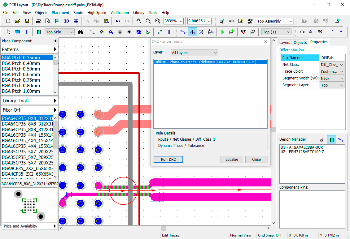
The second error reports that we have phase tolerance violation and it happened on the trace segment that is longer than Dynamic Phase Error Length value in the Net Class parameters. We need to make the shorter trace a bit longer to fix the phase shift. We'll fix the error with Phase Tune tool. Press  button on the High Speed toolbar or go to "High Speed /Differential Pair Tools / Phase Tune" from the main menu. In the pop-up dialog box, you can check which track needs phase tuning. Hover over the bottom track of the differential pair with the mouse cursor and notice that Forward Point Phase Lead value is highlighted in red and the software suggests to add or increase the meander at the opposite trace.
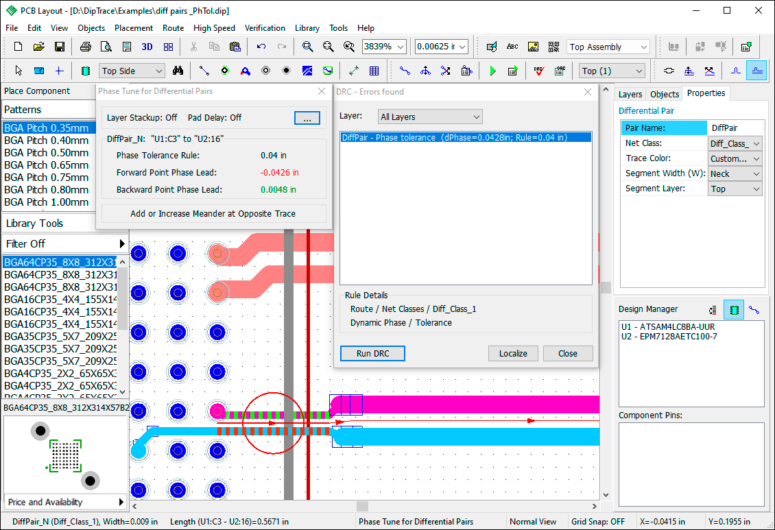
Now hover over the opposite trace. We see that the signal in the upper trace is a bit faster than in the lower one. Left-click on the upper trace, and move the mouse cursor up while holding the left mouse button to create a meander. Release the mouse button when the meander is ready. Because there is a backward point phase lead on this trace, you need to have a meander closer to the U1 component, but not too close to avoid very sharp turns that are bad for the signal. Don't make a meanders too big. They have to be just enough to fix the phase shift and not to cause any "uncoupled length" errors.
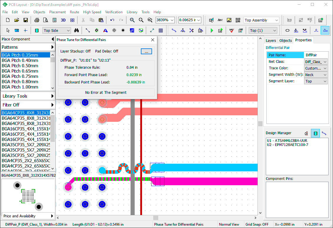
Press Run DRC to check the design again and make sure that all errors are fixed.
If you hover over a trace segment with the mouse and find out that some phase lead violation is still shown in Phase Tune for Differential Pairs dialog, but DipTrace does not report it as an error upon running DRC, it means the segment is shorter than Dynamic Phase Error Length value set in the Net Class parameters. So, you still have a phase shift, but it occurs on a relatively short trace segment well within the tolerance limits.
You can edit meander size anytime later, just press button on the Route toolbar, and drag and drop the meander's tip.
Notice that DipTrace can calculate a phase shift considering layer stackup (via height) and the length of bonding wires inside a component (determined by the Signal Delay).
By default, DipTrace does not consider these values. If you want to consider them, press button in the Phase Tune for Differential Pairs dialog box, and check the corresponding items in the pop-up dialog box. However, this is not important in our case, because there are no differential pairs crossing the layers in our design.
66. Differential Pair Manager
If you have a complex design with lots of differential pairs, it becomes hard to manage them directly on the design area. DipTrace has Differential Pair Manager which allows for easy managing/editing/deleting differential pairs. Select "High Speed / Differential Pair Manager" from the main menu. In the pop-up dialog box, set specific net class in the Net Class drop-down to display only the pairs of the net class, or select All Classes to show all pairs of the design in the list right below. However, this does not make any difference in our case, because we have only two differential pairs of the same net class.
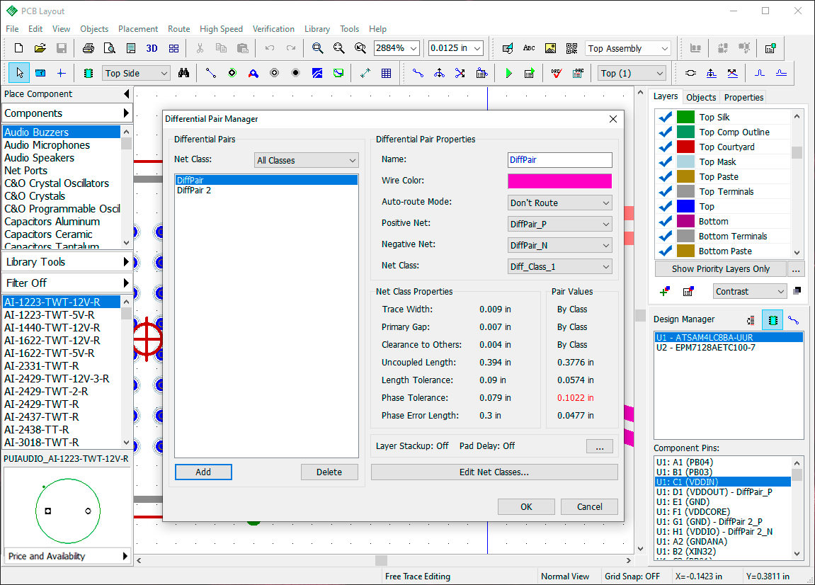
Press Add to open Define Differential Pair dialog box and create a new differential pair, or select existing one from the list and modify its name, color, nets, net class, etc. Right below you can see the Class Properties and Pair values if this differential pair is routed. Red-highlighted value is the violation. In our case Phase shift on selected differential pair is bigger than the tolerance, but it is not considered an error unless there is a Phase Error Length violation.
67. Define paired pads
On rare occasions for the circuit boards with lots of various differential pair pads located very close to each other, DipTrace might not be able to draw two traces and finish routing the pair. In this case, you will get a warning message that offers to use Define Paired Pads feature.
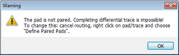
Here is a typical situation. We have R6 and R10 pads that belong to the positive net and R11, R7 pads of the negative net of the differential pair. It is possible that the software in such case can terminate the second trace on the R7 pad (not on the R11), or either drop the warning message.
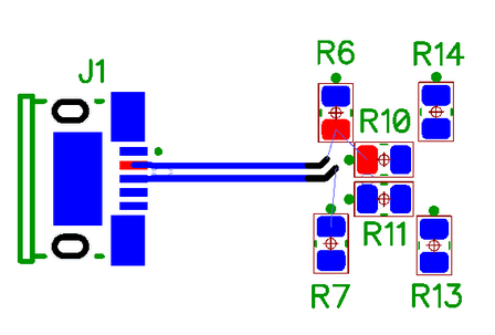
To fix this issue, you need to group the pads. Go to "High Speed / Define Paired Pads" from the main menu. In the pop-up dialog box use the Differential Pair drop-down list to select the pair. You can press Update button to let the program find pads automatically, or check Manually checkbox and define the pair of pads using the lists right below.
We have one pair of pads on the side of the J1 connector (J1:2 and J1:3). Select R10:1 from the Positive Net list and R11:1 from the Negative Net list, because we want the differential pair to terminate on these pads. Then press the left arrow button to add selected pads to the Paired Pads list, and press OK to apply changes.
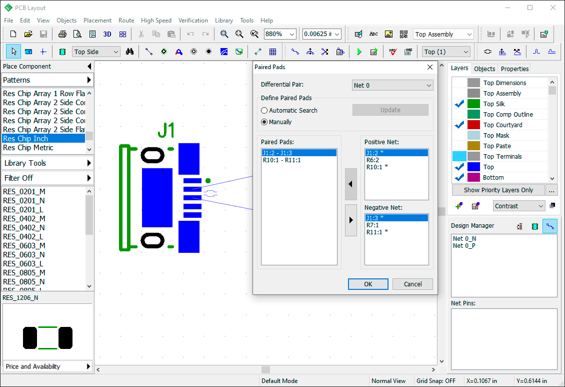
Now route the differential pair. Everything works fine because the software clearly knows, where you want to connect the differential pair nets. Finally, draw two traces from the R6 and R7 pads to their respective nets.
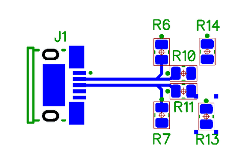
Schematic-PCB synchronization
68. Renew layout by schematic
Sometimes electronic designer needs to make important changes to the circuit board, for example, to add a new net or a component. We always recommend to start implementing those changes in the Schematic, but they do not automatically appear in the PCB Layout, you need to launch Renew Design from Schematic to automatically update existing circuit board according to the schematic.
If you made changes in the Schematic and want to bring them to PCB Layout, select "File / Renew Design from Schematic" from the main menu in DipTrace PCB Layout, then select one of available renewing modes:
1) By components means using the hidden IDs to determine component-to-pattern links – this mode works only if the circuit was created in DipTrace Schematic. Renewing by components doesn't depend on Reference Designators, therefore, they can differ in the schematic and on the PCB.
2) By RefDes means that component-to-pattern links are determined only by Reference Designators. Components must have the same reference designators on the circuit board and in the schematic.
3) Related Schematic means renewing by components from a related schematic file (go to "File / Layout Information" from the main menu if you don't remember the source-schematic file).
Now select the schematic file, and press Open. DipTrace will keep component placement and current routing on the circuit board. New components appear near the board outline ready for placement.
69. Back annotate
Back Annotation allows the user to update schematic according to the PCB file. This feature is useful when you've made changes directly on the circuit board and want to keep the layout and schematic synchronized. Use it with caution, because the Back Annotation, unlike the Renewing from Schematic, has certain limitations.
Launch DipTrace PCB Layout module, then open "PCB_2.dip" file from the "Examples" folder. Use Design Manager to find C8 and C10 capacitors. Right-click on the components in the list, and select the first item from the submenu to change the reference designators of C8 and C10 capacitors to C28 and C30. Select "File / Save As" and save this PCB as another file, for example, "PCB_2_ver1".
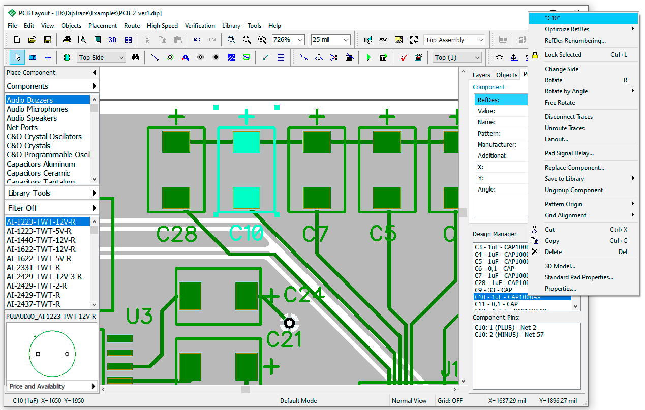
Close the PCB Layout and open Schematic Capture again (notice that you can open it directly from the PCB Layout by selecting "Tools / Schematic" from the main menu.
Open "Schematic_2.dch" file and find C8 and C10 components. You can use the Design Manager or press Ctrl+F, then type in "C8", and press Enter to find the component. C8 capacitor appears highlighted in the center of the screen.
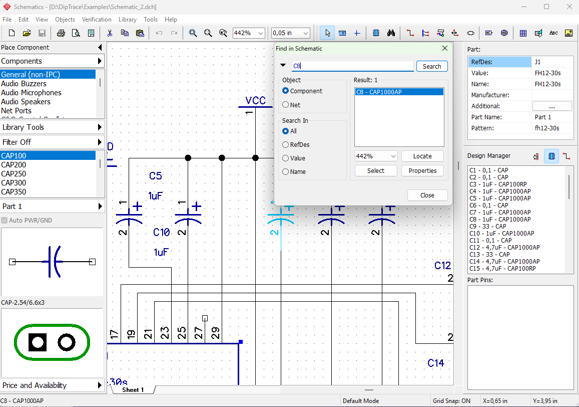
Notice that you can minimize the Find Object dialog box by clicking the arrow in its upper-left corner and use this dialog while editing the circuit.
Zoom on the design area to see C8 and C10 components better. PCB_2 is the circuit board related to Schematic_2, but as you remember we have renamed C8 and C10 capacitors directly on the board. Of course, we can rename that components manually in the schematic or use the Back Annotate feature.
Go to "File / Back Annotate" from the main menu, and select the PCB file where we saved modified copy of the PCB_2 board ("PCB_2_ver1" in our case), then press Open. Now you can see that all designators in the Schematic (in our case C28 and C30) are changed according to the PCB.
Notice that net names and net classes are also back annotated from the PCB, but this feature has limitation and is not capable of adding new nets or components.
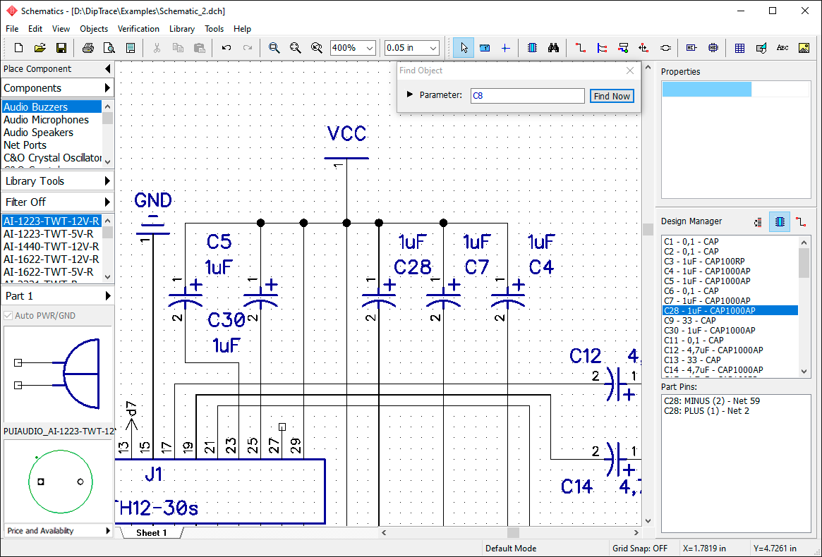
Advanced schematic features
70. Hierarchical schematic
We will design a very simple two-level hierarchical schematic just to show you how this feature works in Schematic and PCB Layout modules of the DipTrace.
Hierarchy blocks
Launch DipTrace Schematic. Hierarchy blocks are associated with sheets, so, first of all, we have to add two sheets to the blank schematic, select "Edit / Add Sheet" from the main menu twice. Then specify that additional sheets are hierarchical blocks, not just regular schematic sheets, select the second sheet in the bottom-left corner of the design area, and go to "Edit / Sheet Type / Hierarchy Block" from the main menu. Do the same for the third sheet.
Select main (the first) sheet, and place several components there (for example, three MAX6050AEUR-T components from the IC PMIC Voltage References library). This will be the main circuit. It doesn't have any hierarchy blocks yet.
Select the second sheet, then go to "Object / Hierarchy / Place Connector" from the main menu or press  button on the Objects toolbar, and place several hierarchy connectors to the second sheet (notice that you can not place hierarchy connectors to non-hierarchical sheets).
These connectors are the inputs and outputs of the hierarchy block, position and rotation of the connectors is the location of the hierarchy block pins on the main sheet.
Place eight connectors, four on the left side and four on the right. Add two diodes from the Diodes RF library, connect them to the connectors, leave some free space for the upcoming hierarchy block of the second level. Use R hotkey to rotate hierarchy connectors.
Select Sheet 3, and create the second hierarchy block here. Place several hierarchy connectors (two on the sides and two at the bottom), add couple components (for example, two AD1856RZ components from IC Data Acq DAC library), and connect them.
Notice that you can rename hierarchy connectors in the right-click submenu (select the first item from the drop-down menu). Connector name will be the name of the block's pin on the main circuit.
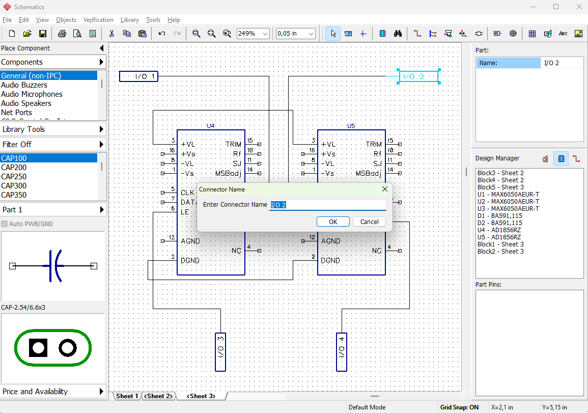
DipTrace supports multi-level hierarchy, i.e. hierarchy blocks can be inserted into the main circuit and into each other as many times as needed.
Select Sheet 2, then go to "Objects / Hierarchy / Place Block" or press  button on the Objects toolbar. In the pop-up dialog box containing the list of available hierarchy blocks, select Sheet 3, and place two blocks (Sheet 3) into the second sheet (Sheet 2). Use R to rotate blocks.
Notice that you can place Sheet 2 inside itself or make a closed loop of hierarchy blocks, but it is an error. To avoid this situation, use "Verification / Check Hierarchy" from the main menu. DipTrace PCB Layout also checks hierarchy for closed loops and displays the warning message when you open schematic with hierarchical errors.
We are not making any closed loops right now, just place two Sheet 3 blocks into the Sheet 2, and connect them to connectors like in the picture below.
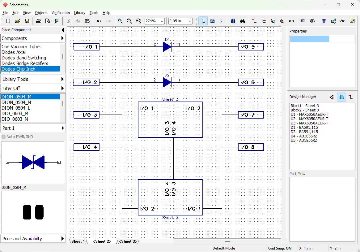
You can rename hierarchy blocks just like regular sheets, right-click on the corresponding sheet tab in the bottom-left of the design area, and select Rename from the submenu.
Select the main sheet, and place hierarchy blocks to the main circuit (for example, add two Sheet 2 blocks and one Sheet 3, like in the picture below). Connect hierarchy blocks with other components of a schematic.
Notice that hierarchy blocks are similar to regular components, they have pins and you can rotate or move them around the design area.
This circuit is not a real-life project, it's just a demo example for this tutorial.
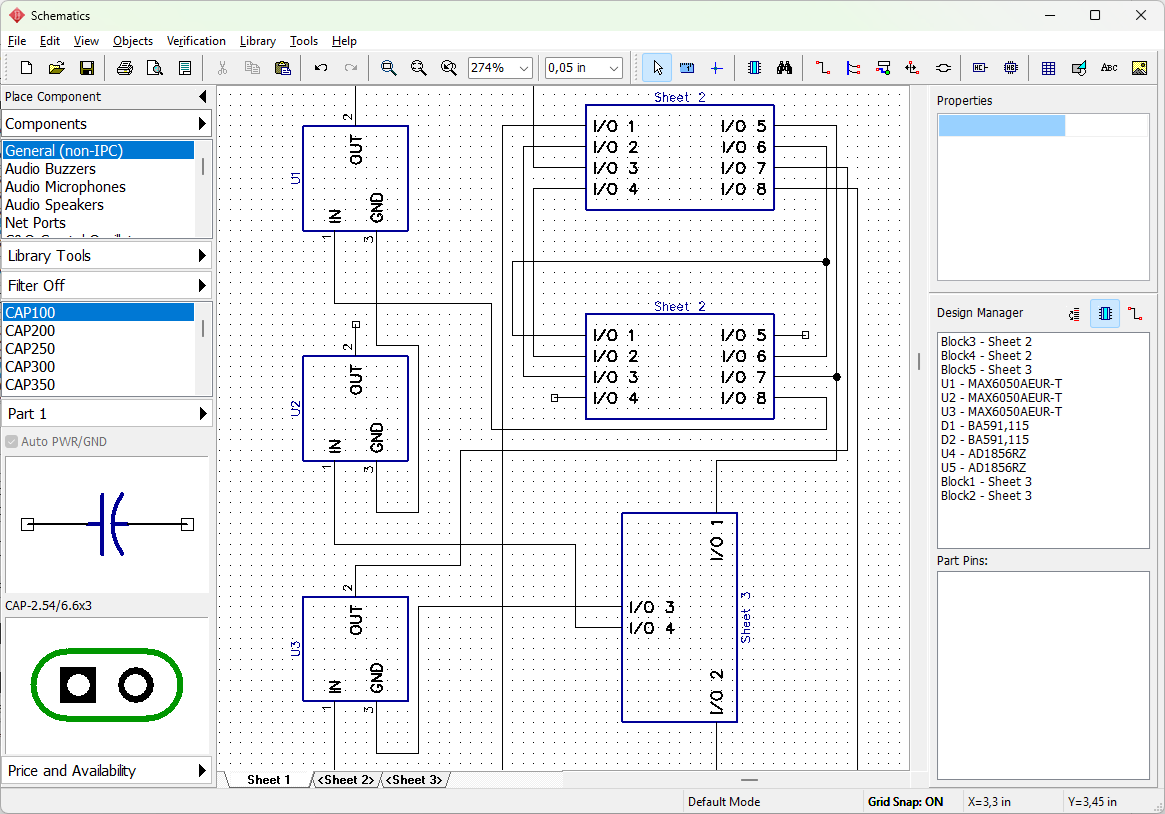
Global nets
As you already know, pins on different levels of hierarchy can not be connected with a single net, unless it is a special-type net called "global". Global nets exist on different levels of hierarchy and do not depend on the hierarchical structure of the schematic.
Return to Sheet 3, and place a ground (GND) net port from the Net Ports library, then connect it to DGND pins of U4 and U5 components. Notice that the net has automatically become global.
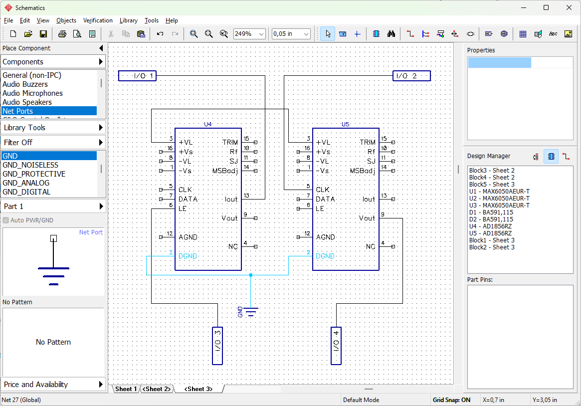
Select Sheet 1 (the main circuit), and place GND net port there, then connect it (create a wire from the net port to some free GND pin). You'll notice that this net now becomes Net 30 (Global). We have a single global net on two hierarchical levels. We can continue this net into Sheet 1 etc. Rename net to "GND".
Notice that the same net ports anywhere on the circuit are automatically connected to a single net (Global – if in the hierarchy).
You already know how to connect nets by name, creating global nets does not differ much. Right-click on a random net, and select Properties from the submenu. In the pop-up dialog box check Global Net for Hierarchy, and Connect Nets by Name checkboxes. Type in the name of the global net that already exists, and press OK.
Hierarchy in the PCB Layout
Convert this hierarchical schematic to PCB. Press Ctrl+B, and select Use Schematic Rules. In the PCB Layout module components that were in the hierarchy blocks are superimposing each other, arrange them with button on the Placement toolbar).
Notice that all components have the same reference designators as in the Schematic + the hierarchical block index.
Go to "View / Component Markings and mark RefDes in the Show column to display the reference designators if they are hidden.
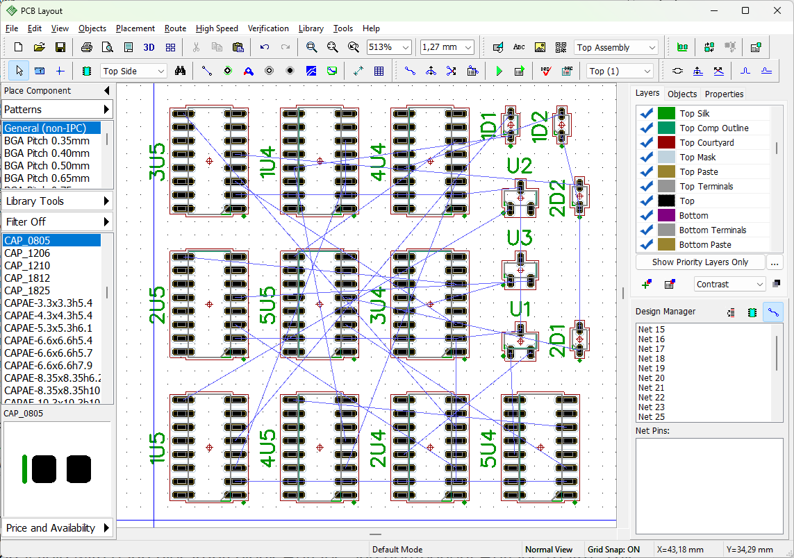
Right-click on one of the components that belongs to a hierarchy block, and select Properties from the submenu. Notice that component involved in the hierarchy has an additional field with each hierarchy block RefDes and component RefDes (path). This additional field is used while updating the PCB by RefDes ("File / Renew Design from Schematic" from the main menu).
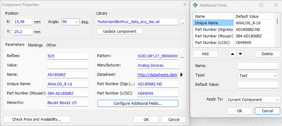
DipTrace works with hierarchy circuits in the PCB Layout module. You can automatically arrange components by hierarchy blocks and apply routing and component placement from one block to another similar block. On the printed circuit board all components, regardless of their hierarchy level, are on the same layer.
Select "Route / Hierarchy" from the main menu. There are two hierarchical sheets available (the same as in the Schematic). Select Sheet 2, and you will see two actual hierarchy blocks (because Sheet 2 was inserted two times into the main circuit in the Schematic). Select Sheet 3 and you will see five blocks inside it (because Sheet 3 was inserted two times into each Sheet 2 hierarchy block, and inserted once directly into the main circuit in the Schematic). Notice that the name of the block of higher hierarchical level is listed in the brackets. When you select a hierarchical block from the list, you can see components and nets that belong to this block on the right in the Block Content field.
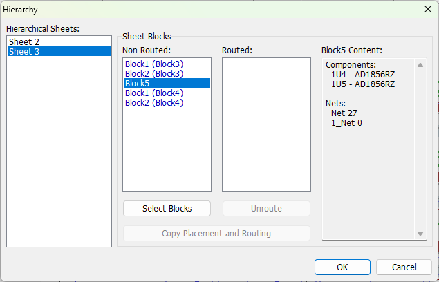
None of the blocks is routed so far.
First of all, we need to arrange components by blocks on the circuit board, select hierarchy block in the list and DipTrace highlights its components on the design area.
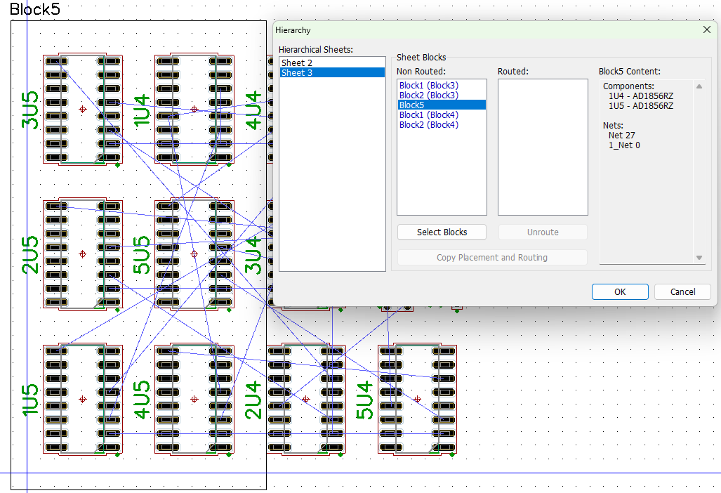
Press Select Block button to arrange components by selected hierarchy blocks.
We will arrange components of the two hierarchy blocks on the board, select Block3 and Block4 from the Sheet 2 (use Ctrl to select two blocks at a time), press Select Blocks button, and then press OK to close the dialog box and apply arrangement. Now the two blocks of components are clearly visible on the design area. We will work with Block 3, which is right below the Block 4.
Change the layout of components in the Block 3 and route traces automatically, do not route global nets. Since GND is a global net, we need to exclude the GND net from the autorouting. Right-click on GND net in the list on the Design Manager panel, select Net Properties from the submenu, and in the pop-up dialog box specify Auto-route Mode: Don't Route. Press OK to apply.
Notice that global nets should be routed only after finishing routing and arranging components in the hierarchy blocks.
Now let's route the traces, right-click on component pad, and select Route Net from the submenu or right-click on the component, and select Route Traces to route all nets of this component. The autorouter automatically creates a rectangular board outline. Edit traces manually, if you need.
Notice that we didn't autoroute the entire board: only the traces inside the Block 3, some connections to Block 4, traces to components from the main schematic sheet.
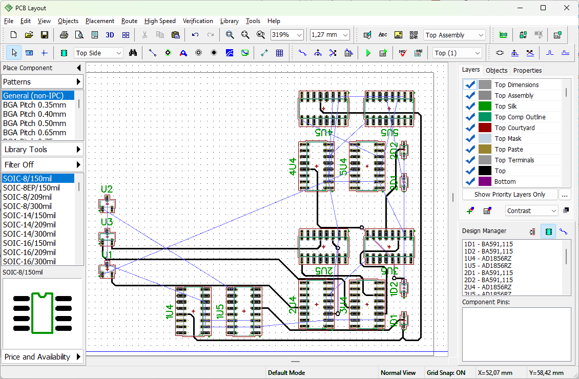
Copy placement and routing between hierarchical blocks
Go to "Route / Hierarchy" from the main menu, select Sheet 2 again. This time, Block 3 is routed. Select Block 3 from the Routed list, and Block 4 from the Non Routed list, then press Copy Placement and Routing button to apply Block 3 placement and routing to the Block 4.
If you have routed many traces from Block 3 to Block 4, the Block 4 can appear in the Routed list in the hierarchy dialog box. Just select it, and press Unroute, then apply routing and placement.
Let's also apply placement and routing to Block 5 without closing the Hierarchy dialog box. Select Block 5 on the Sheet 3, and then select one of the routed blocks, then press Copy Placement and Routing button again. Now press OK to apply routing.
Routed blocks are next to the board outline, use box selection to move them on the design area.
Notice that DipTrace did not copy traces heading outside selected hierarchical block.
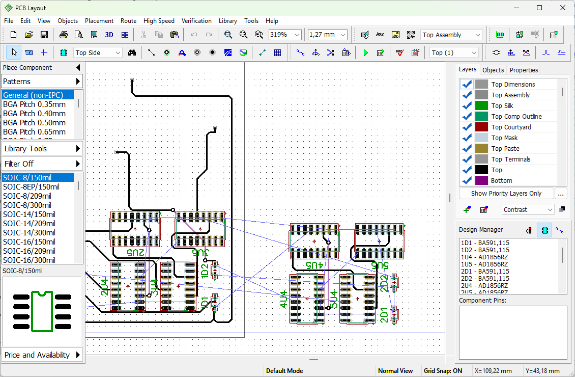
71. NGSPICE simulation
DipTrace features a built-in NGSPICE simulator and allows the user to define SPICE settings for the components in the Schematic Capture and Component Editor modules. We are going to run a simulation of the Astable Flip Flop circuit, but before that we have to make sure that SPICE models have been defined for all the components of the schematic.
SPICE Model
Launch DipTrace Schematic, and open "C:\ Users\<UserName>\Documents\DipTrace\Examples\Spice\Astable_Flip_Flop_Spice.dch" file. We have already defined all the SPICE settings for this circuit. However, let's review a couple of the components just to learn how to set up SPICE models. Right-click on the C2 capacitor, and select SPICE Model from the submenu. Spice settings for capacitors are pretty simple: select Model Type: Capacitor, enter values into the parameters table (in our case "22µF "), and specify positive and negative pins (enter values into the pin-to-signal table in the central part of the dialog box, the list of available signals is right below). Notice that you can enter parameters directly into the table cells.
The Template field shows how this component is represented in the SPICE netlist. You can scroll that field to the right if it is long. Make sure that settings are like in the picture below.
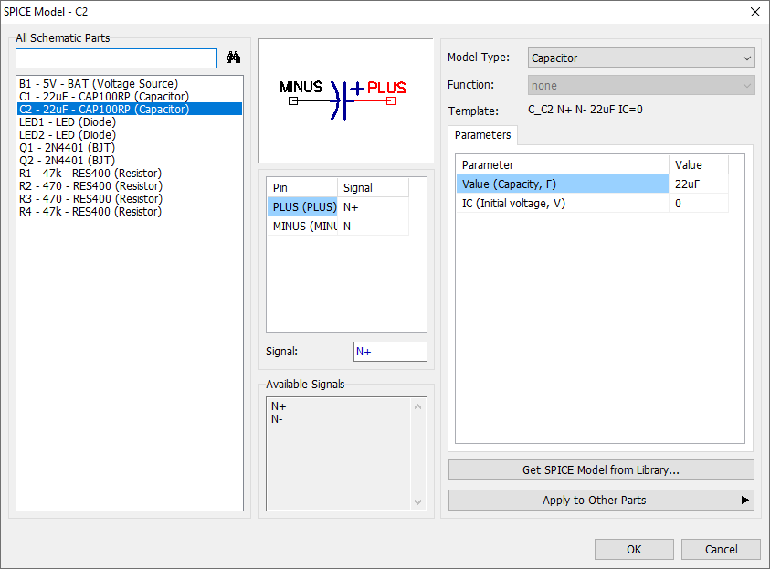
Select another model type, for example, a Current Source. The user can specify a function for this model type. Use the Function drop-down list and select PWL(). In the pop-up dialog box enter the number of points for PWL function, and click OK. Now you can enter the values for each point in the Parameters table. Different functions require different parameters (amplitude, phase, etc.). See detailed description in the SPICE language documentation.
Now return to the Capacitor model type, and discard any changes.
Setting up SPICE Model
Capacitors do not require additional model description, but transistors do. Select Q1 transistor from the list of All Schematic Parts, now you can see that for transistor there is also a Model tab near the Parameters tab, select it. Now you can enter the model text or load the SPICE model from an external file (Load and Save buttons). Some component manufacturers publish SPICE models for their components on the web.
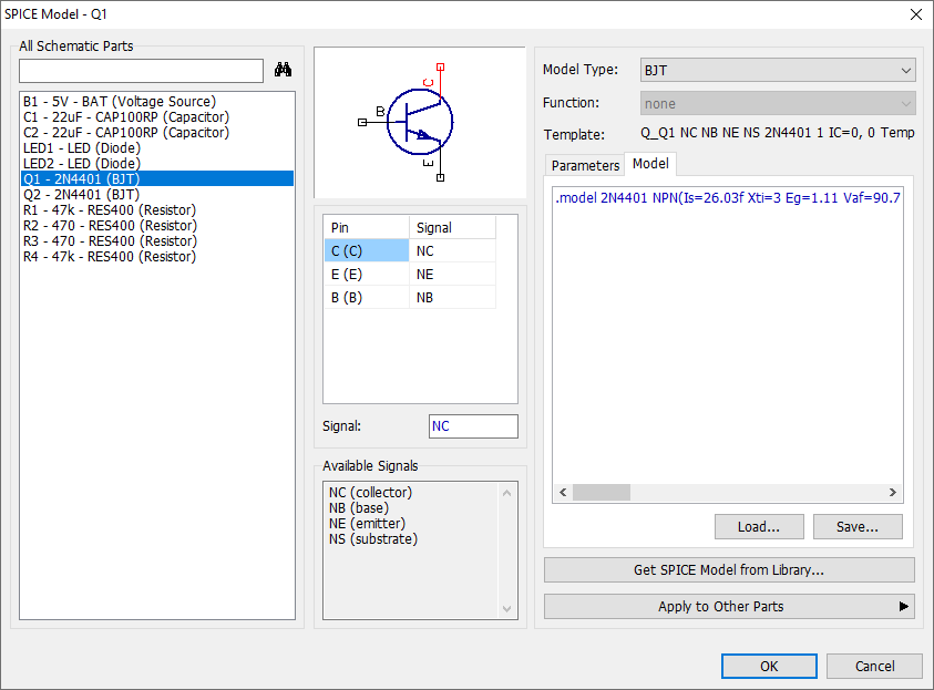
Notice that you can get all SPICE settings from another DipTrace library (use Get Spice Model from Library button) or apply the current settings to All Similar Parts of the Component or Schematic (Apply to Other Parts button).
There is no valid SPICE model for the power source (battery) in the Astable_Flip_Flop_Spice.dch file, we should define it. Click on the B1 component in the list of All Schematic Parts. You can see that the component has the Voltage Source model type, but no valid function. Set Function: PULSE(), then specify the following parameters in the table below: Pulse V2=5, Pulse PW=20s, Pulse PER=30s. Keep other parameters, and press OK. Now we have the voltage source that produces 5V during the first 20 seconds, then there is a 10-second interval. Now everything is ready for simulation.
SPICE Simulation
Once SPICE models of the components are defined, we can run a simulation. Go to "Tools/ SPICE Simulator". In the left part of the pop-up window you can see several tabs for simulations of different types. The last one is Digital. Select it Transient tab and set Start Time: 5, Step: 0.1 s, Stop Time: 20 s. GND Net is selected correctly. Now press Run Simulation Button, after that select a couple of signals (I (LED 1) and I (LED 2), for example) in All Signals list, use  button to add a selected signal to the simulation graph and
  to remove it.
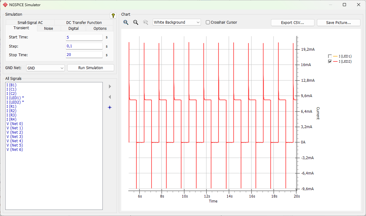
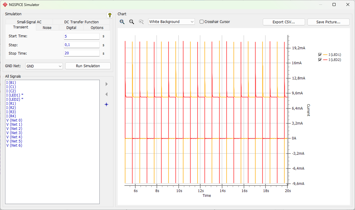
The tracks show that LEDs flash on and off alternately, which means that the circuit works fine.
For more details about SPICE simulation please see Schematic Help.
Digital Spice Simulation
To run a SPICE simulation for a digital circuit in DipTrace, the process is straightforward and similar to simulating analog circuits.
For this tutorial, we'll use a pre-made schematic from the DipTrace examples. Start by opening the "RS-trigger" project, which can be found by default at C:\User\Documents\DipTrace\Examples\Spice\RS-trigger.dch.
Before diving into the simulation, make sure SPICE models are configured for all components in your circuit. Right-click on U1:1 and select SPICE model from the submenu. In the pop-up window make sure that Digital:Nand model is selected. Note that in addition to basic models, DipTrace also supports more advanced behavioral models, including analog, hybrid, and digital types.
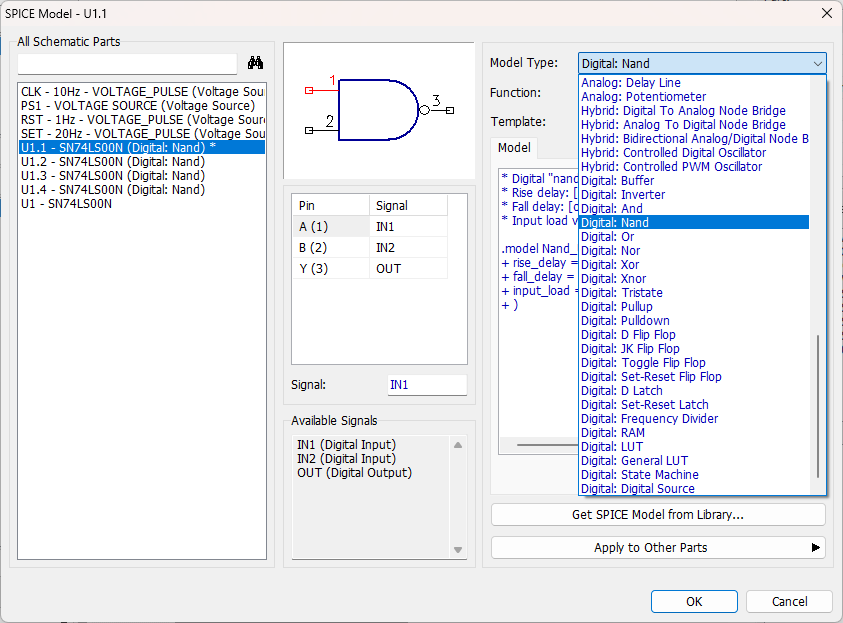
Once all models are correctly defined, you can move forward with the digital SPICE simulation. Navigate to the Tools menu and select SPICE Simulator.
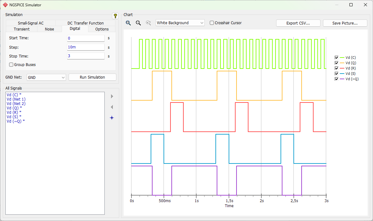
In the SPICE Simulator window, you'll notice several tabs in the upper left corner, each corresponding to different types of simulations. For our purposes, select the Digital tab. Next, configure the simulation parameters: set the Start Time to 0, the Step to 10ms, and the Stop Time to 3s. Make sure that the GND Net is selected correctly.
Now, you're ready to run the simulation. Click the Run Simulation button to initiate the process. After the simulation runs, you'll want to visualize the results. In the All Signals list, select the signals you wish to display. Use the button to add the selected signals to the simulation graph. If you need to remove any signals from the graph, simply use the button.
Unlike the analog simulator, where signals are drawn one on top of the other in an appropriate scale, digital signals are displayed in multiple rows. This allows you to track the changes of several signals simultaneously. In more complex circuits with buses (e.g., D0..D7), you can display a hex value instead of drawing each bit separately (using the Group Buses option).
This process allows you to analyze the behavior of your digital circuit in a detailed and interactive way, providing valuable insights for refining your design.
Export SPICE netlist
In DipTrace you can also export a SPICE Netlist to run a simulation using, for instance, LT Spice, which is free simulation software of a good quality.
|
Select "File / Export / Spice Netlist" from the main menu. In the small pop-up dialog box select GND from the GND Net drop-down list. Specify Commands: .TRAN 0s 30s 0.1s to simulate the circuit from 0s to 30s with 0.1s step. Notice that you can define/change commands directly in the simulation software. Click OK and save the *.cir netlist file. Launch the SPICE simulator that you have. We will use LT Spice as an example (download it at Linear Technologies website). |
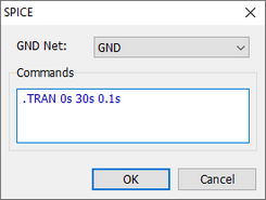
Select "File / Open" and open the *.cir netlist that you just saved (notice that you should select correct Files of Type). Now you can see the netlist in the text format. Select "Simulate / Run" from the LT Spice main menu, and close the error-log dialog. Select "Plot Settings / Visible Traces", and choose I(D_led1) to see electrical current on LED1. This component works during the first 20 seconds, then has 10 sec interval. Select other signals to see how they work.
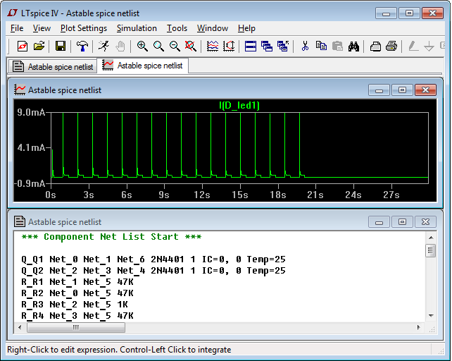
Design rules and verification
72. Saving/loading design rules
In the Converting to PCB topic of this tutorial, we mentioned that you could use Schematic rules or load rules from any PCB layout project while converting schematic to the PCB. No need to specify all layers, net classes, via styles, and design constraints again. Let's see how it works.
Create a new layout, select "File / New" from the main menu or press Ctrl+N hotkeys. In the pop-up dialog box, you can choose to create an empty layout or use settings from the previous project.
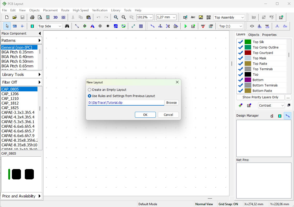
Check Use Rules and Settings from Previous Layout, press Browse, and select the *.dip or *.dipxml file of the circuit board that contributes its settings for a new layout. Press OK. In our case, we have selected the *.dip file of the project that we have created in the first part of this tutorial. Layer colors and some DRC settings have changed.
In the DipTrace PCB Layout, you can save settings in the special file, separately from the layout itself. Just go to "Route /Save Rules" from the main menu, enter the file name, and press Save. Now you can use rules and settings from this file while creating new projects. Go to "Route / Load Rules" and choose the *.dip, *.dipxml or *.rul file.
Please add some via styles, a new net class with random parameters, GND and PWR inner layers and save this as a *.rul file. We will use it later in the Fanout topic.
73. Electrical Rule Check
Electrical Rule Check (ERC) feature is one of the main verification features in DipTrace. ERC checks the circuit for pin type conflicts, unconnected and superimposing pins as well as one-pin nets and short circuits.
Launch DipTrace Schematic and open Schematic_2.dch from the "Documents/DipTrace/Examples" folder. Define electrical rules, select "Verification / Electrical Rule Setup" from the main menu. In the pop-up dialog box specify incompatible pin-to-pin connections and the program's reaction to them (error, no error or warning, depending on the color) by clicking in the grid cells with green, yellow and red squares.
Pin Type checkbox in the Rules to Check section means checking pin-to-pin connections defined in the grid;
Not Connected Pins – the program searches for unconnected pins;
Pin Superimposing – the program searches for pins overlaying each other;
Only One Pin in Net – the program reports nets with only one pin, i.e. net that makes no sense. It can be a potential error in the net structure;
Nets With Single Pin – the software searches for nets that include only one pin.
Short Circuit – the program reports any connections between Power and GND nets. Let the software know which net is POWER and which one is GROUND in the Power Pins for SC section below.
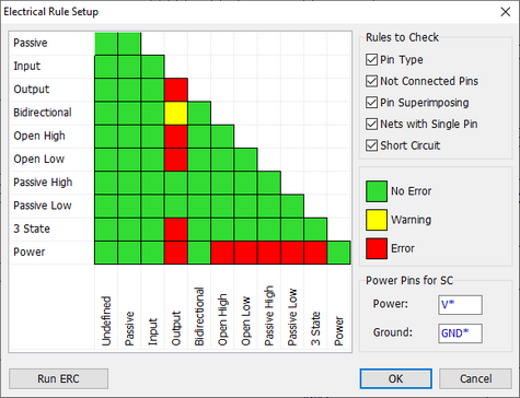
Press OK to close the dialog box.
Now select "Verification / Electrical Rule Check (ERC)" from the main menu. If you verify "Schematic_2.dch" file, according to the rules from the picture above, you should get many error reports in the list: one warning for Bidirectional to Output connection and a lot of Not Connected pin errors. To localize error on the schematic design area, double-click it in the list (or press Localize). You can fix errors without closing the ERC report dialog box. Press Run ERC button to start verification again.
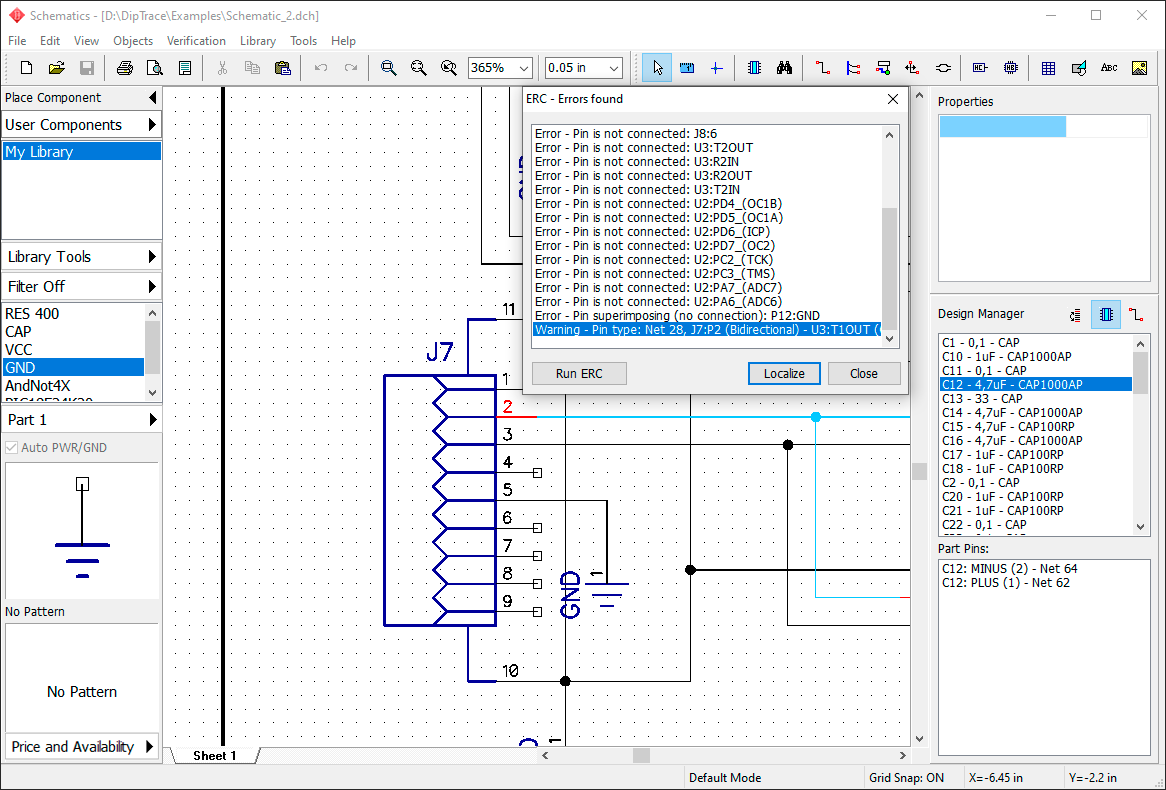
ERC does not report errors for pins, which are intentionally unconnected. Right-click on one of these pins, and select Not Connected from the submenu. Alternatively, you can uncheck the corresponding item in the ERC settings dialog box, but then the possibility of an error increases, because all unconnected pins are now OK, even if it is not supposed to be that way.
74. Checking net connectivity
This type of verification allows the user to check if all nets on the circuit board are connected. Net connectivity check reports broken connections and isolated copper areas (not depending on the connection type: traces, thermals, shapes, or copper pours).
Launch the PCB Layout module, and open "PCB_2.dip" file from the "C:\ Users\<UserName>\Documents\DipTrace\Examples" folder. Go to "Verification / Check Net Connectivity" from the main menu. In the pop-up dialog box you define the objects that will be considered as connectors by the verification algorithm, typically we recommend to keep all checkboxes checked. Press OK to launch verification.
The circuit board does not have any unconnected nets. Therefore, we will make two errors intentionally.
Close the error-log dialog box, press button on the Route toolbar, then move the mouse to the trace that connects C16:2 to the via and GND copper pour in the Bottom layer, right-click on this small trace segment, and select Unroute Trace from the submenu. This is going to be our first error.
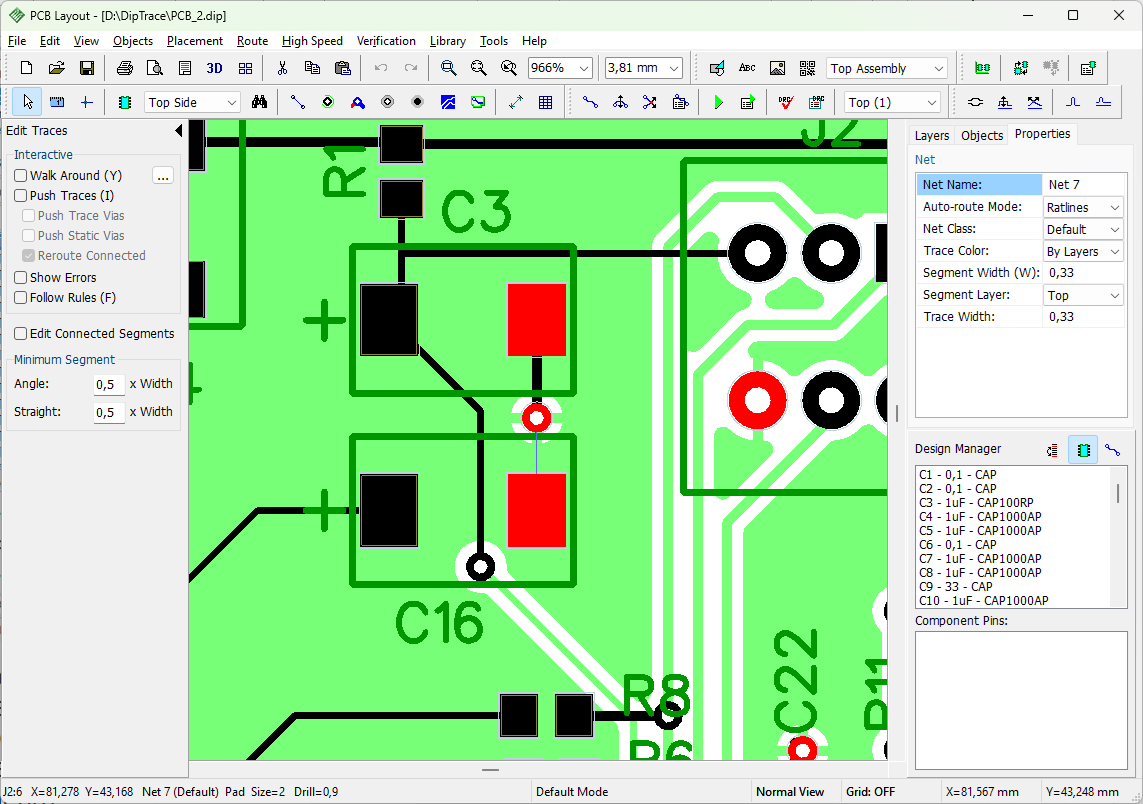
Isolated copper pour area is the second error that we are about to commit. Double click on the Bottom layer, then pan to the bottom-right corner of the circuit board, and draw a couple of shapes (arcs or lines) to isolate one of the vias, and don't forget to update the copper pour (right-click on the copper pour's outline, and select Update from the submenu).
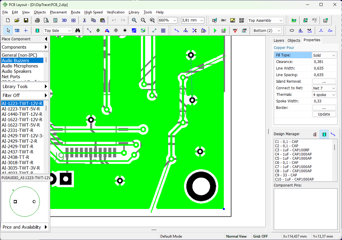
The picture shows a simple situation when it's very easy to find the mistake, but most errors of this type (isolated copper pour areas and non-connected pins) usually go unnoticed on complex circuit boards.
Go to "Verification / Check Net Connectivity" from the main menu, and click OK in the pop-up dialog box. The verification reports a broken-net error. Click on the error in the list, and check error Details. We have Net 7 broken to 4 unconnected areas, scroll down the Details section of the Connectivity Check Results dialog box to see all unconnected areas of the net and component pads sorted by areas. Area 1 is the biggest, it is the main part of the copper pour, the second area is that C16 capacitor's pad which trace we unrouted at the beginning of this topic, the Area 3 appeared as the result of isolating the part of the copper pour at the bottom-right of the circuit board.
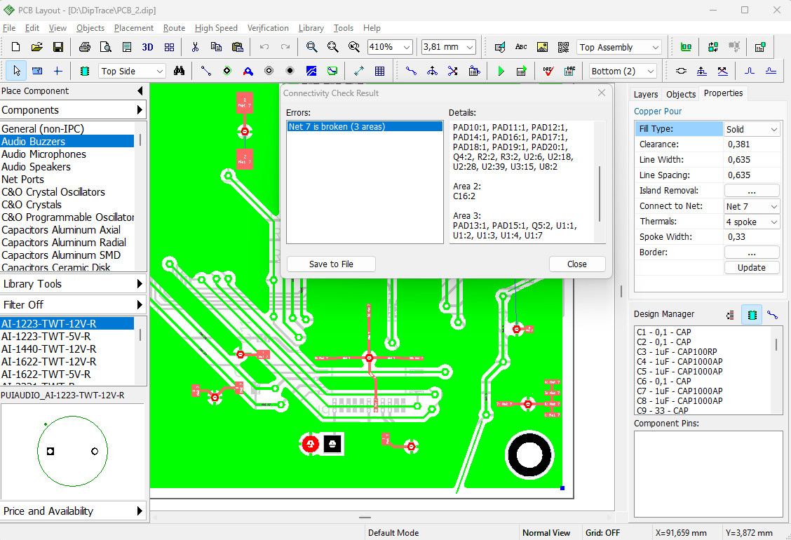
You don't have to close the Connectivity Check Results dialog box to fix errors, just move it a bit.
Sometimes it's hard to understand how to find and fix errors on the design area. We recommend using the Design Manager for easy navigation. Just scroll down the list of components and double click on the component in the list to highlight it on the design area.
You can also save the net connectivity error report into the text file.
Routing techniques
75. Fanout
Fanout allows the user to automatically connect pads of the selected components (BGA, SOIC, QUAD) or SMD pads of the selected net to inner plane layers with vias of a certain style.
Open the PCB Layout module or if it is already open, select "File/ New" from the main menu. Load rules from the *.rul file that we created at the end of Saving/Loading Design Rules topic of this tutorial. It should have the default, through-hole, and blind/buried via styles, custom net class, and two inner plane layers.
Fanout a component
Now select Patterns library group, it contains all patterns available in standard DipTrace libraries. Notice that these are just the patterns without schematic symbols. Place one PLCC20P127_990X990X457L203X43N from the PLCC Pitch 1.27mm Square library and two BGA100CP50_10X10_600X600X100B30N from the BGA Pitch 0.50 mm library. We will use these patterns for demonstration, but you can select another patterns/components for practicing with fanout.
Right-click on the PLCC pattern, and select Fanout from the submenu. In the pop-up dialog box specify: Pattern Type: SOIC/QUAD, Placement: Outside, Pads: Left (this means that only the left row of the pads will have fanout vias), and make sure that Use Connected Pads Only checkbox is unchecked (because we want to have fanout vias for all pads of the component, regardless of whether they are connected or not).
Select different Via Styles for the pads on the top and bottom side of the board (inactive if there are no pads on that side). Preview parameters of the existing via styles by pressing the Via Styles... button. In our case we have three via styles: one with through-hole vias, another with blind/buried vias and the Default via style with relatively big vias. Select the one which fits the size of the current component (Default via style in our case).
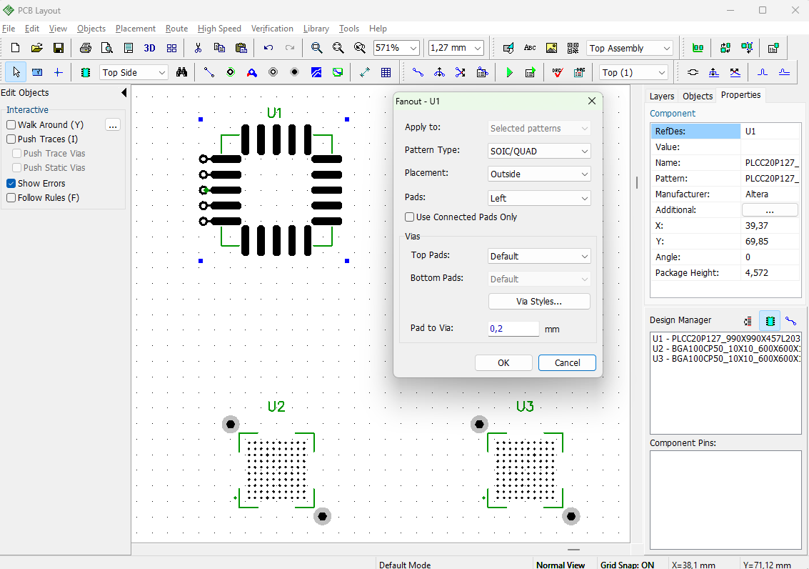
|
Press OK, and vias will appear outside the left pad line of the PLCC pattern. Right-click on the same pattern, and select Fanout again. Now we will place zigzag vias for the top pads. Set: Placement: Zig-zag and Pads: Top, keep other settings, and click OK. Now we will make through-hole vias for one of the BGA patterns and blind/buried vias for another. Make sure that you have the corresponding via styles first. BGAs will need smaller vias (we used 0.3 mm vias with 0.15 mm holes for this example).
|
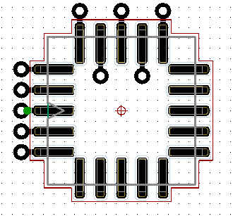
Right-click on the first BGA pattern, and select Fanout from the submenu, specify Pattern Type: BGA – All pads and select custom via style with through-hole vias. Press OK.
Now select the second BGA package. Right-click it, and choose Fanout from the submenu. Set Pattern Type: BGA - By rows. This allows the user to apply different via styles to different pad rows of the same pattern or even exclude some rows from the fanout. Left-click on the row number, and select Via Style from the drop-down list.
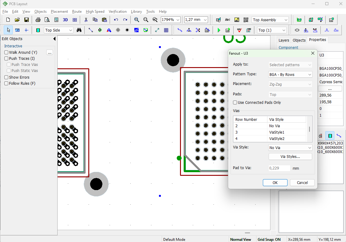
|
We will not create vias for rows #1 and #2; you can use different via styles for different rows. Press OK. We can see, that for the first BGA pattern all pads are connected to vias, for the second pattern – first two rows are without vias, |
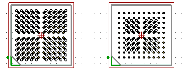
because these are usually connected on the top layer of the board.
Fanout net
We will connect several SMD pads to the GND plane layer using the Fanout feature. Place several SMD and a couple of through-hole patterns on the design area. Create a net that connects some pins of these components (we suppose this is our GND net that we should connect to the GND plane layer). Select "Objects / Place Ratline" from the main menu or press button on the Objects toolbar to create ratlines (connections). Rename net to "GND" if you want. Check the Ratlines item on the Design Manager's Objects tab if you don't see the ratlines on the design area.
Make sure that there is a via style with blind/buried vias from Top to GND layer, then right-click on one of the connected pads (not on the pattern), and select Fanout from the submenu. In the pop-up dialog box select appropriate via style, and click OK. Now all SMD pads of selected net have vias connecting them to the GND inner plane layer, where we have placed a copper pour connected to GND net.
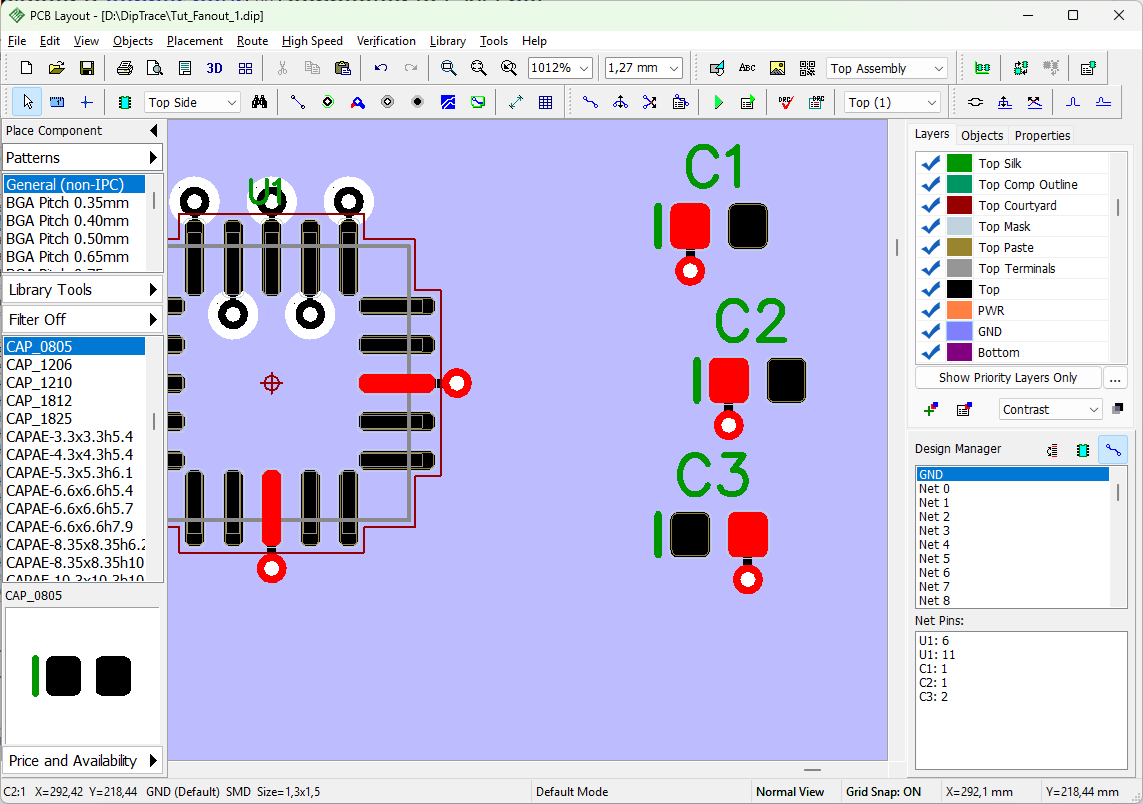
76. Via Shielding
Via Shielding is a technique used in PCB design to improve signal integrity and isolate sections of the board operating at different frequencies. This is achieved by placing rows of vias along a trace, which helps protect sensitive signals from interference and crosstalk.
Please note that the Via Shielding tool functions only when there is a copper pour on both the layer where the trace is selected and on at least one other layer. Additionally, both the copper pours and the shielding vias must be connected to the same net for the tool to work properly.
To get started, let's open the "Differential_Pairs" example project in DipTrace. Once the project is loaded, select Net 14, which can be done either by clicking directly on the board or by finding it in the list of Nets on the Design Manager panel. After selecting Net 14, simply right-click and choose Via Shielding from the menu. If you prefer using the main menu, you can also find this option under Objects > Via Tools > Net Via Shielding.
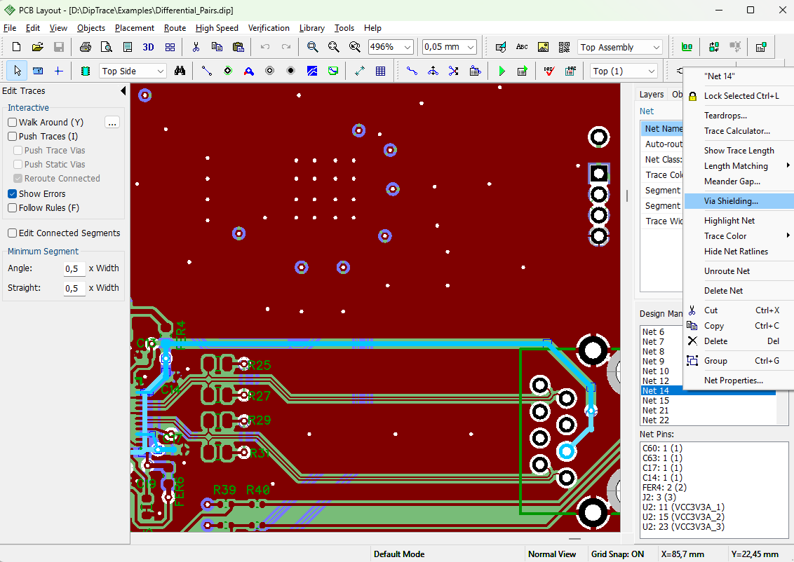
|
We are going to shield only the selected segment of the trace, so in the pop-up dialog choose Add Vias to: Selected Segments. For the via style, we have a few options. We can select any style available in the project from the Via Style drop-down menu, but for this tutorial, we'll stick with the Default style. If you want to review, modify, or even create a new via style, you can do so by pressing the Via Styles button. Next, let’s ensure that the vias are properly connected by setting the Via Net to GND. This will connect the shield vias to the ground net, providing the necessary isolation.
|
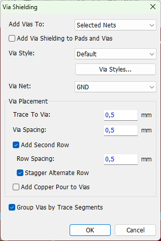
Moving on to the Via Placement parameters, we’ll set the Trace to Via Gap and Via Spacing to 0.5 mm. This ensures that the vias are closely spaced for effective shielding. To add an extra layer of protection, we’ll mark the Add Second Row option, placing a second row of vias parallel to the first. We’ll set the spacing between these rows to 0.5 mm as well and enable the Stagger Alternate Row option to arrange the vias in a staggered pattern, which enhances the shielding effect.
Finally, to keep everything organized, we’ll mark the Group Vias by Trace Segments option. This ensures that the vias are grouped according to the trace segments they are shielding, making the design both effective and easy to manage.
Once all the settings are configured, click OK, and DipTrace will shield the selected net with vias, respecting the parameters you've set and adhering to the PCB design rules.
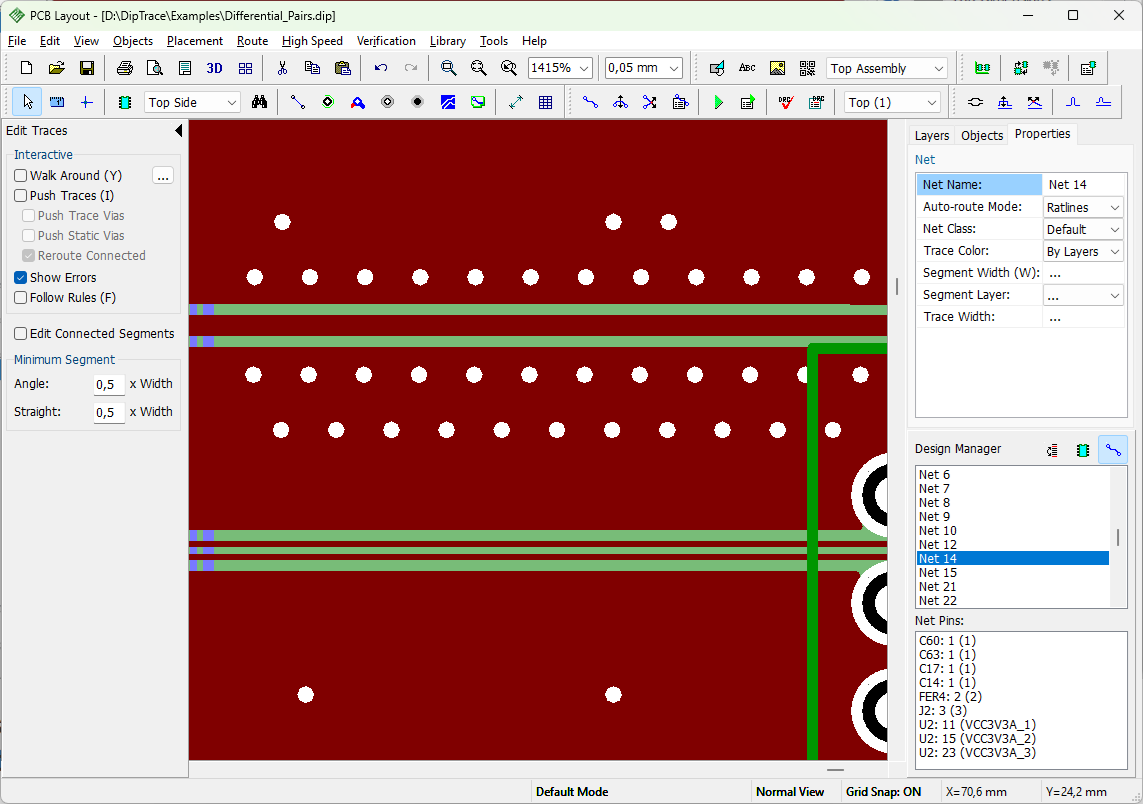
Note that the via shielding algorithm is designed to prevent DRC errors, which may result in some vias being omitted from the via shielding array.
Undo the changes to restore the project and prepare it to practice the use of Via Stitching feature.
77. Via Stitching
Via stitching is a technique used to improve the electrical performance and structural integrity of a PCB by connecting copper pours on different layers through a grid of vias. This helps with grounding, thermal management, and signal integrity by reducing impedance and minimizing interference.
DipTrace provides two options for via stitching: stitching the entire board or a specific area only. Let’s begin with stitching the whole board.
In the "Differential_Pairs" example project, navigate to Objects > Via Tools > Board Via Stitching. In the pop-up dialog, you can choose one of the existing via styles or press the Via Styles button to review, modify, or create a new via style. For this example, we'll use the Default style. Ensure that the Via Net corresponds to the copper pours' net, which is GND in this case.
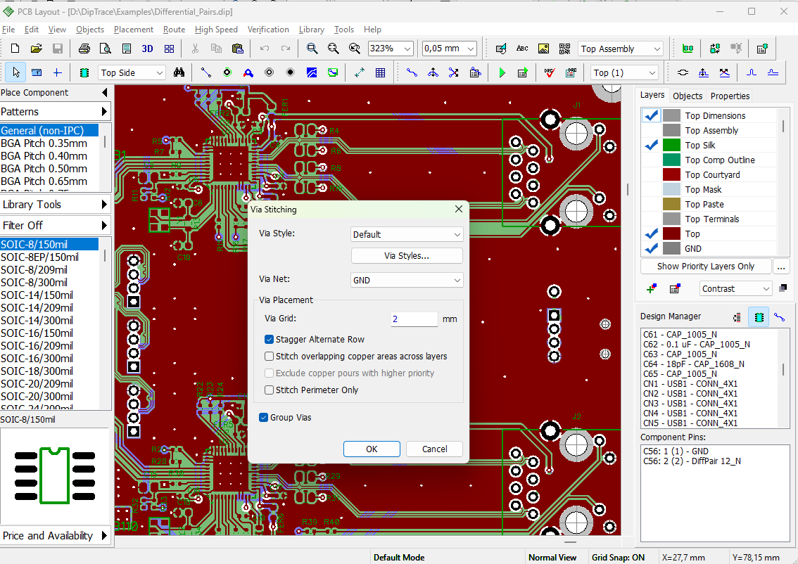
Next, we are going to configure the Via Placement parameters. Set ViaGrid to 2 mm, and mark Stagger Alternate Row to arrange vias in a staggered pattern. Since copper pours cover the entire board in this project, we don't need to mark the "Stitch overlapping copper areas only" option, though it’s useful when dealing with separate copper areas on different layers.
The "Exclude copper pours with higher priority" option prevents stitching copper pours of different priorities, which can be beneficial in more complex designs, but since all our copper pours have the same priority, we can leave it unchecked.
The "Stitch Perimeter Only" option allows placing vias only along the perimeter, without filling the entire area.
Finally, check Group Vias to keep the stitching vias organized. Click OK, and DipTrace will automatically check the design rules and stitch the entire copper pour area with vias.
To prevent vias from connecting to copper pours, update them by selecting Object / Update All Copper Pours.
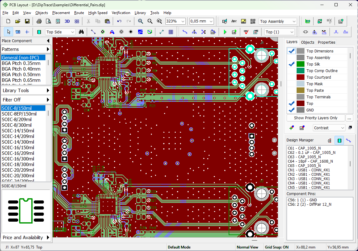
Now let's undo those changes and explore how Area Via Stitching works.
Navigate to Objects > Via Tools > Area Via Stitching. To define the area for stitching, left-click on the copper pour to place anchor points and outline the shape. Once you’ve outlined the desired area, right-click on the final point and select Enter.
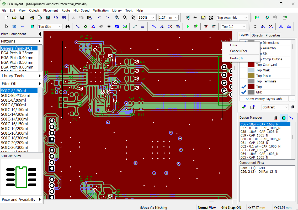
The Via Stitching dialog will appear. We can keep all the previous settings unchanged, select the GND net, and then simply click OK. DipTrace will then stitch the defined area of the copper pour with vias according to the parameters we've set.
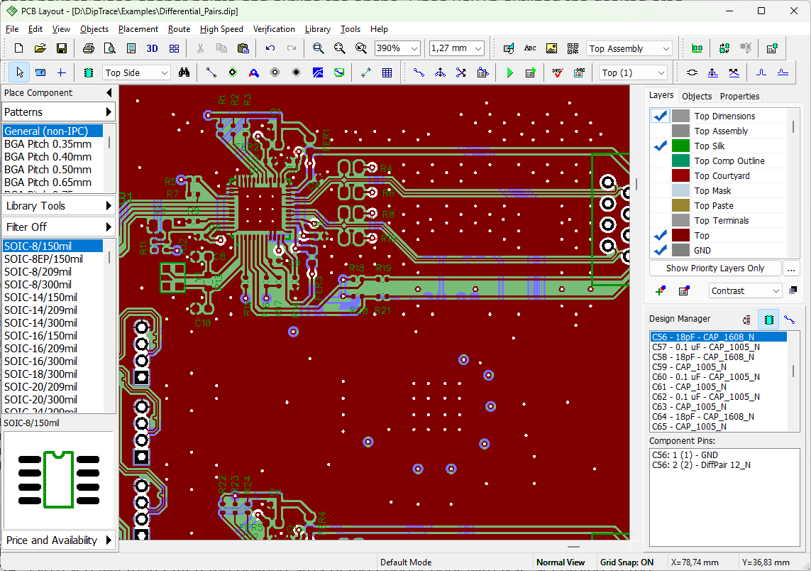
Manufacturing data and documentation
78. Bill of Materials (BOM)
In DipTrace a bill of materials can be generated in the Schematic and PCB Layout modules.This tool is similar in both modules, but has more advanced options in PCB, so let’s see it in more detail.
Open Banana_Pi.dip project from DipTrace examples (C:\Users\Documents\DipTrace\Examples). To create a bill of materials for a printed circuit board, select "File/ Export/ Bill of Materials" from the main menu.
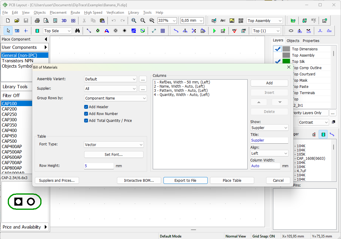
The Bill of Materials dialog allows the user to customize columns and rows, add interactive autoapdating tables to the existing project, save BOM in HTML, Excel CSV or text format with the required table configuration.
To begin with, let’s see how to create and configure several Assembly Variants for the same board. Press button, in the pop-up window press Add and enter the name of the assembly variant. Select any cell in the Variant column and remove blue checkmarks for the parts you don’t want to appear in the BOM of a certain prototype. You can use quick-selection buttons at the bottom of the window: All - to select all components, SMD - to select surface mount components only, Through-Hole - to select all through-hole components.
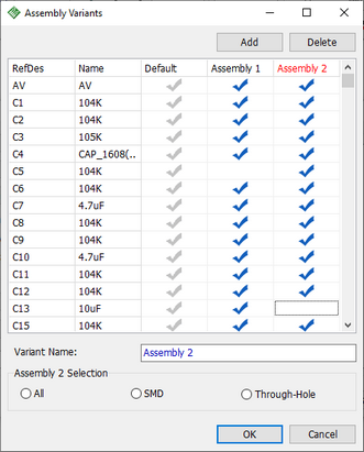
Several variants can be configured at once. When done, click OK to save them. Once created, the Assembly Variants will appear in the drop-down list. Default variant represents the original layout and is not editable.
The Supplier drop-down allows generating BOM based on the Supplier status of the components. You can create a BOM that includes all the components, components from certain supplier or parts to which no supplier has been assigned. The last two options work only if suppliers have been selected for the components of the layout. We have not assigned the suppliers yet, but we can do that right now.
Press Suppliers and Prices button in the bottom-left corner - Suppliers and Prices dialog will pop-up.
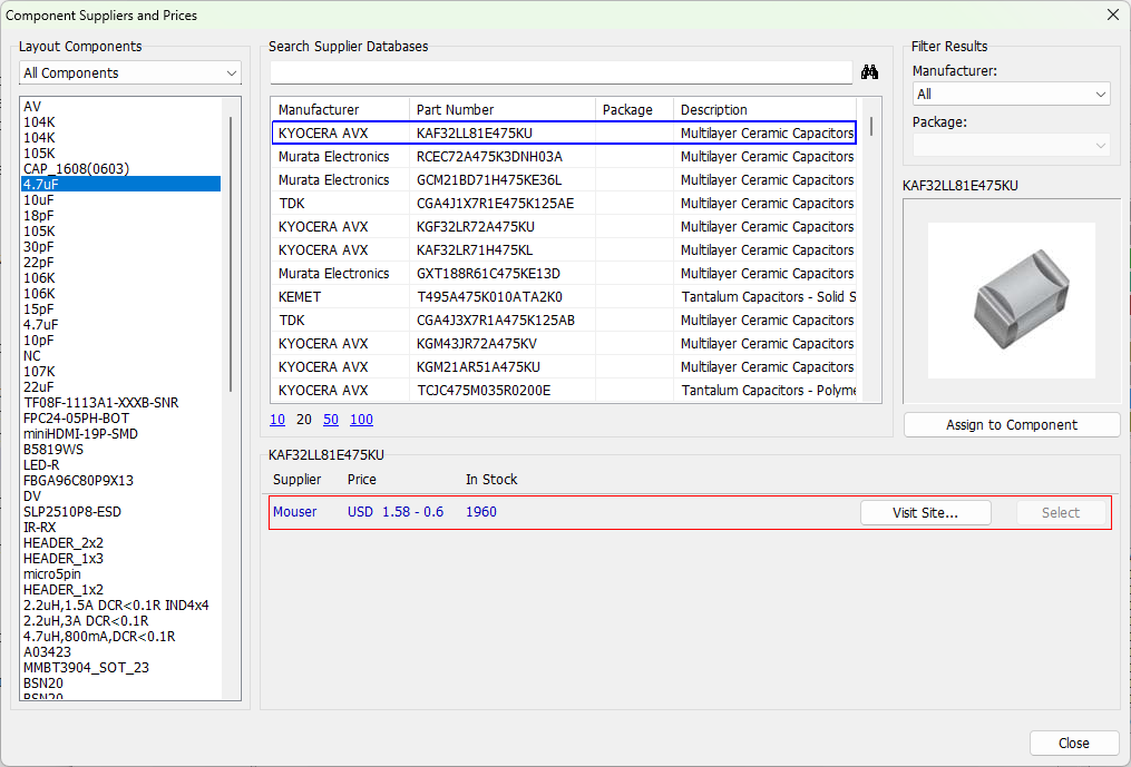
In the Layout Components list select a component. In the central part of the dialog the available parts are shown. We are going to select packages and assign suppliers randomly, just to practice. Press Assign to Component button to confirm the selection of the part and supplier for the current component. Proceed with other unassigned parts, if you want to practice a bit. When done, close the dialog.
For more information please refer to PCB Layout Help (PCB Layout > Objects > Component > Assign Supplier).
Next, let’s configure, how the information will be organized by Rows and Columns in the BOM table.
In the Group Rows by drop-down select Components. Use the checkboxes below to add a header, row number, and total quantity/price of the components.
In the Columns section on the right add columns to the BOM file with the settings like in the picture below. Select the corresponding item (Name, RefDes, Value, Quantity, etc.) from the Show: drop-down list, and press Add button. You can change the order of the items using arrow buttons, add or delete columns from the table. Besides, you can select how the data will be aligned and also specify the width of the columns.
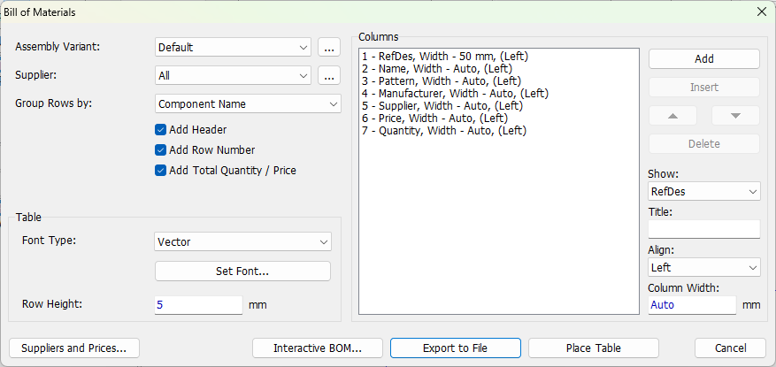
If you are going to place a BOM table directly in the project, use Table section of the dialog to set font parameters and row height. Press Set Font button to customize the font settings. Use only TrueType fonts for Unicode characters.
When you are done with configuring the BOM table you have four different options to create it.
1. Place a Table on the design area. To do that, press Place Table button, and left-click on the design area, where you want the top left corner of the table to be located. An interactive table with all the components will be placed in the Top Assembly Layer.The components selected in the table are highlighted on the board. The table is updated automatically, so can keep editing your layout after placing the table - all subsequent changes will be included into the report.
2. Interactive BOM within PCB Layout - a pop-up table corresponding to the column and row settings will appear. The components selected in the table are highlighted on the board. Press Localize for DipTrace to center the component from the selected row on the design area.
3. Export to File. The BOM files are available in 2 formats: Excel CSV and files with *.bom extension. When exporting to file, DipTrace will ask you to set a Column Divider and decide whether to use Quotation Marks for values or not. Please notice that you can add custom rows and columns to the BOM file in any spreadsheet editor.
4. Export HTML - this option provides for easy BOM sharing and revision outside DipTrace environment. Save HTML file (Interactive BOM / Export HTML) and then open it in your browser.
In the "Placed" column, you can select which components will be installed. You can then save these changes using "Save Batch".
Use buttons in the top-right corner to configure BOM generation parameters, table and layout display mode.
U (Ungroup) - show each component of the circuit board in the BOM separately.
NL (Netlist) - generate a list of all the nets of the circuit.
N (Component Name) - group components in the BOM table by component name.
NV (Component Name and Value) - group components in the BOM table by component name and value.
NP (Component Name and Pattern) - group components in the BOM table by component name and pattern.
NVP (Component Name, Value and Pattern) - group components in the BOM table by component name, value and pattern.
BOM - show BOM table only.
LR - display BOM on the left and layout on the right.
TB - display BOM in the upper and layout in the lower part of the window.
T - show BOM and layout of the top side of the board only.
TB - show BOM and layout of both, top and bottom sides.
B - show BOM and layout of the bottom side of the board only.
79. Importing/exporting netlists
DipTrace allows the user to import and export netlist files of various formats (Accel, Allegro, Mentor, OrCAD, PADS, P-CAD, Protel, Tango). Netlist export can be used to review schematic net structure or board design in other software.
Export netlist
To export netlist from the DipTrace Schematic, select "File / Export / Netlist" from the main menu, select the netlist format, specify folder and file name, and press OK to save the netlist file.
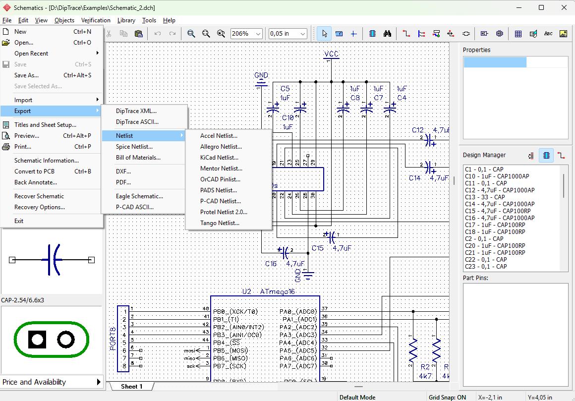
Import netlist
DipTrace PCB Layout allows for importing netlists created in other software. We will import Tango netlist as an example. Launch the PCB Layout, create a new project, and select "File / Import / Netlist / Tango" from the main menu, then select "tango_1.net" file from "C:\Users\<UserName>\Documents\DipTrace\Examples" folder.
As you already know, all components are represented by patterns on the circuit board. The first step while importing the netlist is to make sure that each component has its pattern. Check all patterns in the File Components list:
RefDes column shows component RefDes in the netlist,
Name column shows component's name,
Pattern Name column shows pattern's name from the netlist,
Pattern column shows attached pattern in the DipTrace libraries. If it is blank, the component does not have a pattern.
Press Add button to add new pattern libraries that contain the required patterns. For example, add Cap Chip Inch library to find a pattern for C 225 components. Add several libraries at a time with "Shift" and "Ctrl" hotkeys. DipTrace standard libraries are in the "C:\Program Files\DipTrace\Lib" folder and user libraries – in the "Documents/DipTrace/My Libraries" folder by default.
Select a library, and press Assign all Patterns by Names – the software will find and assign patterns with the corresponding names automatically.
Sometimes DipTrace is not able to find all the patterns, because of partially or completely different pattern names in the DipTrace libraries and in the netlist. In this case, the designer should find and assign all patterns manually. Select a component in the File Components list, then select a library and a pattern from the respective lists. Now press Attach to Component button to attach pattern to the component according to the component's RefDes, name, or pattern name. For example, we will attach CAP_2225_N pattern to all components with CAP 225 pattern.
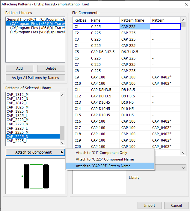
The asterisk symbol (*) after the pattern name in the list means that this pattern was connected manually.
Click Import button when all components have correct patterns.
80. Aluminum Layer stack
DipTrace allows for comprehensive control over the stack of conducting and insulating PCB layers in the Layer Stack dialog box and generates a stackup table that clearly documents the PCB stack for manufacturing engineers.
Launch DipTrace PCB Layout module. By default, the program has two signal layers: Top and Bottom. Select "Route /Layer Setup" from the main menu or press button on the Layers tab, then press the Layer Stack button in the Layer Properties dialog box.
In the Layer Stack dialog box, you can see a table which represents a printed circuit board cross-section. In our case, DipTrace has automatically selected the 2 Layers Default Stack in the Template drop-down list because this design has two conducting layers.
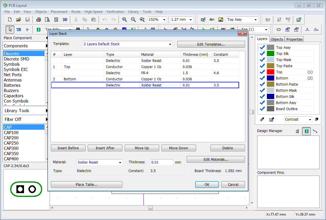
There are a lot of variations of PCB stacks on the market, but default stacks available in the software are usually the most common and thus the cheapest. However, you can create any stackup, even the one that no PCB house would be able to make.
For the purposes of this tutorial we will create a metal-core PCB made of aluminum and capable of conducting big currents. This stackup is often used for LED projects with massive heat output. Unlike FR-4, which is a dielectric glass-reinforced epoxy, aluminum is a conducting material, hence there should be two additional insulating layers of prepreg between the copper layers and aluminum core, like in the picture below.
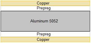
First of all, let's change the copper thickness to 2 Oz to conduct big currents. Usually, it is the thickest copper that does not sky rocket the manufacturing price and available at most PCB houses in stock.
Left-click on the layer #1 Top in the list, and select Copper 2Oz material from the Material drop-down list, then do the same for the layer #2 Bottom. Since two copper layers becomes thicker, the overall board thickness of the circuit board is recalculated automatically.
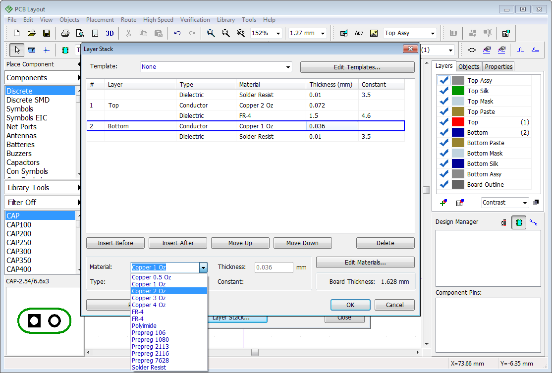
Notice that you can use Shift + U hotkeys to change the measurement units on the go. All values will be instantly recalculated.
Now we need to change the core material to Aluminum. Left-click on the Dielectric type FR-4 material in the stackup list and click the Material drop-down list. DipTrace has a standard set of materials: copper conductors of various weight, FR-4 cores, polyimide for flexible PCBs, prepregs of various weight, etc. As you can see there is no aluminum in the list of available materials, hence we need to add it manually. Press the Edit Materials button. In the Layer Materials pop-up dialog box you can add new and change properties of existing materials (Type, Thickness, and Dielectric Constant). All materials are divided into three basic types: Conductor, Plane, and Dielectric.
Press Add, and enter "Aluminum 5052" in the Name field (it's the cheapest aluminum alloy for rigid metal-core PCBs). Now set Dielectric in the Type drop-down list (of course, aluminum is not a dielectric, but this way it's not confusable with true conducting copper layers). Enter 1.5mm Thickness, and 4.5 dielectric Constant. Check Variable Thickness box to allow for changing the layer thickness directly in the Layer Stack dialog box.
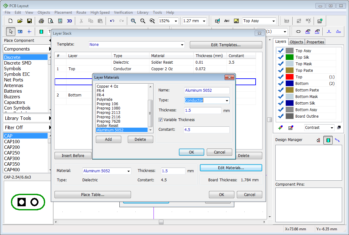
Press OK, and select Aluminum 5052 in the Material drop-down list in the Layer Stack dialog box.
Don't forget to add prepregs to separate aluminum from the copper. Press Insert Before and a blank layer appears before the aluminum core, select this layer, and set Prepreg 1080 in the Material drop-down list (it's a quite thin prepreg that will allow for good heat dissipation). Now add one more prepreg layer after the aluminum core using the Insert After button. The stackup is ready.
The final stage is documenting the layer stackup in the Gerber file for a PCB house. Press Place Table. In the pop-up dialog box, select a non-signal layer for placing the layer stack table Top Assy layer is the best choice. You can change fonts, measurement units and preview the total dimensions of the Layer Stack table.
Notice that you can use Shift + U hotkeys to change measurement layers on the go. All values will be instantly recalculated.
Press Place and left-click on the design area to place a Layer Stackup table in that spot. The color of the table depends on the color of the PCB layer.
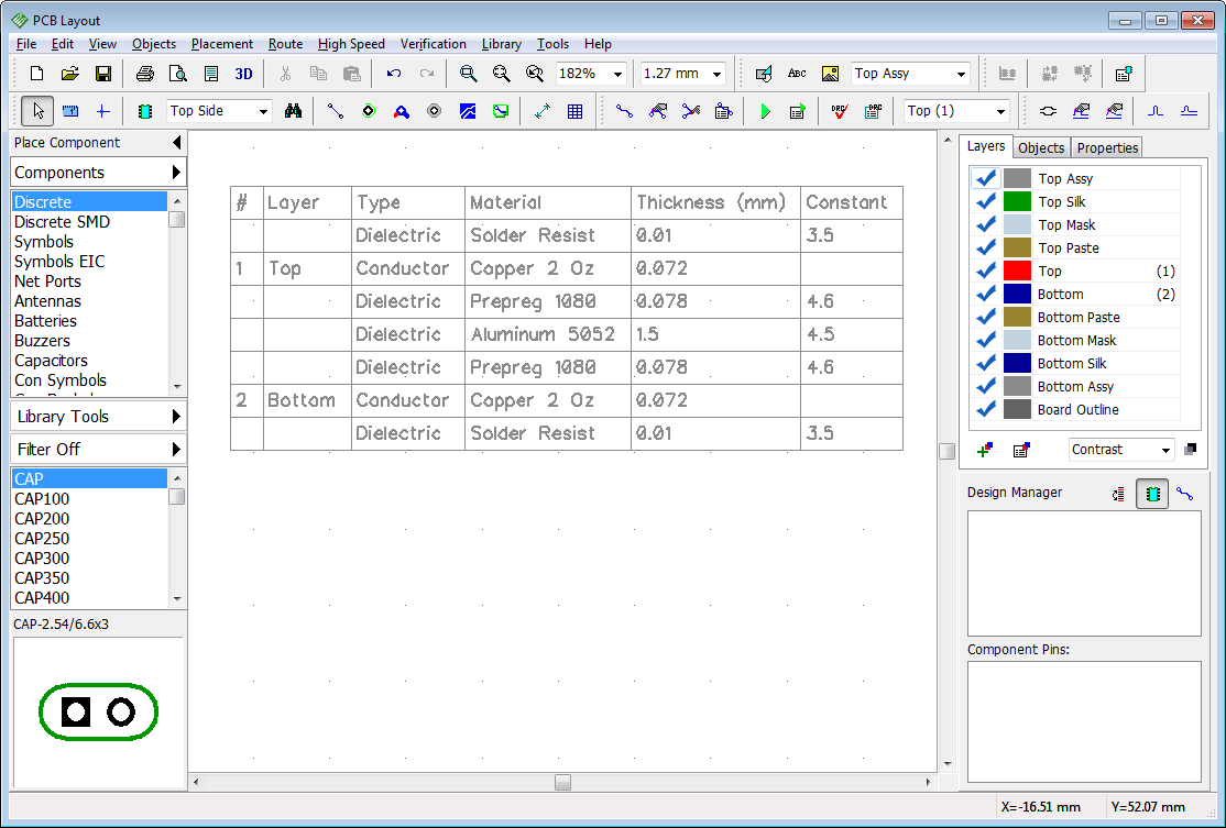
The thickness of the layers in the stack influences the via height and is taken into account by phase tune and trace length measuring tools.
Before making any changes to the stackup please consult your PCB manufacturer.
81. 3D preview and export
DipTrace PCB Layout module features built-in real-time 3D visualization with STEP and VRML export. This tool allows the user to visually check the circuit board with all components installed and export the PCB model to mechanical CAD programs for developing the device housing etc.
Download and install 3D model libraries from the DipTrace website. Components without 3D models appear only as footprints on the circuit board in the 3D mode.
Launch PCB Layout then go to "File / Open" (or press Ctrl+O) and select "C:\Users\<UserName>\Documents\DipTrace\Examples\PCB_6.dip", then press  button on the Standard toolbar. The Attached 3D Models dialog box will pop up. DipTrace checks if all components have 3D models and tries to find correct models for components without them.
See 3D preview and export section in the PCB Layout Help ("Help / PCB Layout Help" from the main menu) for more details.
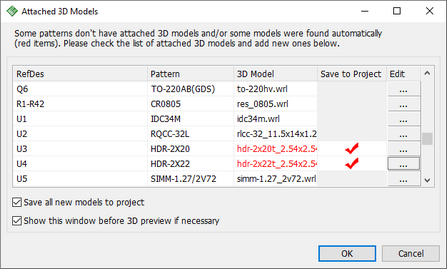
You can change colors of the background, board, solder mask, copper and silk screen display options, just press Redraw to implement the changes.
Press OK, and you'll see a 3D model of the circuit board. You can rotate the circuit board model by three axes, move it with your mouse, zoom in and out with the mouse wheel, etc.Orthographic view can be enabled by selecting the "Orthographic" checkbox.
Note that the general settings of the mask are defined in the Gerber export window.
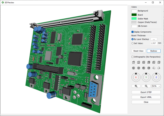
3D export
|
DipTrace 3D Preview module allows the user to export 3D model of the board to STEP (*.step) and VRML 2.0 formats (*.wrl) supported by most mechanical CAD software. When in the DipTrace 3D preview & export module, press Export STEP. In the pop-up dialog box, specify which objects to include in the exported model (Board, Package models, Pad holes), and whether to export the model as a solid body or as parts. |
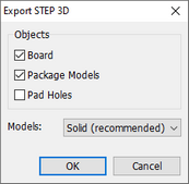
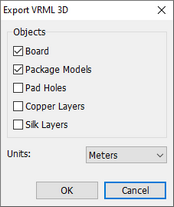
Press OK to specify a filename and folder. We recommend exporting a project as a Solid body in STEP format.
Notice that exporting holes dramatically slows the process.
To export the board model to VRML format, press Export VRML button, select which objects to include in the exported model, set the units, press OK, and define the file location.
Previewing and mapping component 3D model
Press  button in the Attached 3D Models dialog box or right-click on any component on the design area in the PCB Layout, and select 3D Model from the submenu. In the pop-up dialog box, you can rotate a 3D model by three axes, zoom in and out, move the model by holding the right mouse button, and change colors of the preview.
If you need to change a 3D model, press All Models>> button, and select a 3D model from the list of all available models sorted by pattern libraries.
To attach a 3D model from the separate file, press the button to specify the path to the file on your computer. DipTrace supports 3DS, VRML, STEP, and IGES files.
If Pattern Generator was used to create the 3D model you can preview it by selecting IPC-7351 Model Generator option from the drop-down in the upper part of the dialogue.
3D model can also be automatically generated based on the component outline - by Component Outline option. To use this option, an outline of the footprint has to be placed in Pattern Editor. After that you only have to specify the model height and DipTrace will create a 3D shape to mimic a device.
DipTrace automatically places a 3D model to fit the pattern's drawing, but sometimes you may need to adjust a 3D model location or its scale. Just enter appropriate values into the corresponding fields (shift, angle, and scale for each axis). Changes apply instantly. Check out Attaching a 3D model topic of this tutorial and PCB Layout Help for more details about mapping a 3D model.
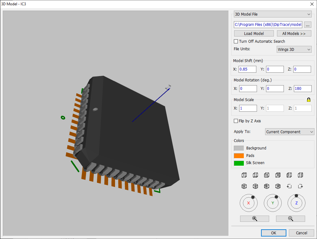
Press OK to close the 3D Model dialog box.
Search 3D models
Go to "Tools / 3D Preview / Patterns and Models Search", in the pop-up dialog box you can change the search accuracy and active search folders.
In the Pattern Search section, you can select the level of conformity that will be used by DipTrace while searching for the models (more strict requirements mean less possible models found). Press Search 3D Models... to check the results.
If you have 3D models in other folders on your machine, you need to let the software know that it should search 3D models in those folders, just add a new folder to the 3D Model Folders list. By default, all 3D models are in the "models3d" folder inside the "DipTrace" directory.
Notice that standard 3D libraries are not included in the DipTrace installation package. You need to download them from the DipTrace website.
We recommend attaching 3D Models in the Pattern Editor when making footprints.
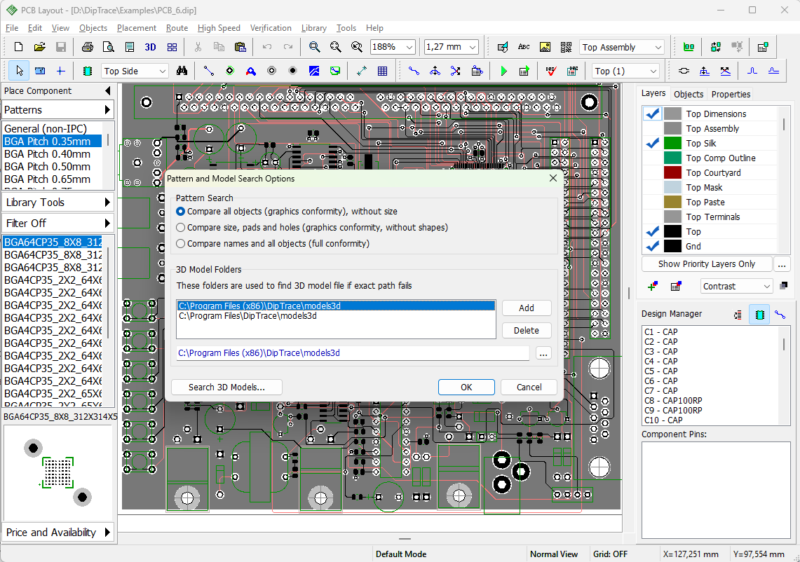
Novarm Ltd., July 2026